Enhanced specular Andreev reflection in bilayer graphene
Abstract
Andreev reflection in graphene is special since it can be of two types, retro or specular. Specular Andreev reflection (SAR) dominates when the position of the Fermi energy in graphene is comparable to or smaller than the superconducting gap. Bilayer graphene (BLG) is an ideal candidate to observe the crossover from retro to specular since the Fermi energy broadening near the Dirac point is much weaker compared to monolayer graphene. Recently, the observation of signatures of SAR in BLG have been reported experimentally by looking at the enhancement of conductance at finite bias near the Dirac point. However, the signatures were not very pronounced possibly due to the participation of normal quasiparticles at bias energies close to the superconducting gap. Here, we propose a scheme to observe the features of enhanced SAR even at zero bias at a normal metal (NM)-superconductor (SC) junction on BLG. Our scheme involves applying a Zeeman field to the NM side of the NM-SC junction on BLG (making the NM ferromagnetic), which energetically separates the Dirac points for up-spin and down-spin. We calculate the conductance as a function of chemical potential and bias within the superconducting gap and show that well-defined regions of specular- and retro-type Andreev reflection exist. We compare the results with and without superconductivity. We also investigate the possibility of the formation of a p-n junction at the interface between the NM and SC due to a work function mismatch.
I Introduction
Andreev reflection (AR) - a scattering process by which a current can be driven into a superconductor (SC) from a normal metal (NM) by applying a bias within the superconducting gap - was first discovered by Andreev andr64 and has been extensively studied for several decades btk ; kasta . Graphene on the other hand has attracted a huge interest in the past decade owing to its electronic and material properties novoselov04 ; neto09 ; rozh16 ; mccan13 . Graphene is a semimetal whose electronic structure can be described by a Dirac Hamiltonian (with a vanishingly small mass). Andreev reflection has been studied both theoretically bhatta06 ; beenak06 ; benjamin08 ; rainis09 ; majidi12 and experimentally sahu16 in graphene. What makes Andreev reflection in graphene special is that it can be of two types: one where the reflected hole retraces the path of the incident electron (called retro-) and another where the reflected hole moves away not tracing back the path of the incident electron (called specular-) beenak06 ; sahu16 . Specular Andreev reflection has not been observed in graphene due to charge density fluctuations across the sample sahu16 , but a weak qualitative agreement is observed in bilayer graphene efet16 ; efet16-prb . Bilayer graphene (BLG) ludwig07 is a better candidate to observe specular Andreev reflection since charge density fluctuations are much smaller than in monolayer graphene. In the experimental setup, a part of the BLG is kept in proximity to a SC, which induces superconducting correlations on BLG. It can be seen in Fig. 3(a) of Ref. efet16 which shows only a weak qualitative agreement between the experimental observations and underlying theoretical calculations (note also the very different color scales of the experimental and theoretical plots required to arrive at even this level of agreement).
Generally speaking, Andreev reflection is a process where an electron incident from a normal metal into the superconductor results in a reflected hole. This is equivalent to saying that two electrons on the normal metal side- one from above the Fermi energy and one from below the Fermi energy pair up and go into the superconductor as a Cooper pair btk . We use the latter convention for our analysis.
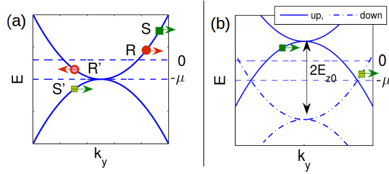
In a manner similar to that for Andreev reflection in monolayer graphene beenak06 , retro- and specular- Andreev reflection can also be understood in bilayer graphene efet16 ; efet16-prb . If both the electrons participating in the reflection come from the same side of the charge neutrality point (CNP), the Andreev reflection is of the retro type, while if the two electrons come from opposite sides of the CNP, the Andreev reflection is of the specular type. This is because, the momentum of the reflected hole along the -direction has to be same as that of the incident electron. This means that when the hole originates from the same side of the CNP as that of the incident electron, the velocities along the -direction of the two electrons participating in Andreev reflection have opposite signs. On the other hand, when the hole originates from the opposite side of the CNP as that of the incident electron, the velocities along the -direction of the two electrons participating in Andreev reflection have the same sign. This is shown in Fig. 1(a).
Furthermore, the two electrons must have opposite spin. This allows us to separate the CNPs for the up-spin and the down-spin bands by applying a Zeeman field. In this work, we add a Zeeman field to the NM part of the NM-SC junction on BLG and calculate the conductance spectrum as a function of chemical potential and bias energy. As shown in Fig. 1(b), for small chemical potential () and small bias () the Andreev reflection is specular. We discuss several features of the conductance spectrum in the presence of a Zeeman field, where the main highlight is the enhanced specular Andreev reflection (SAR) at zero chemical potential and zero bias energy.
The paper is organized as follows. In Sec. II, the calculation is presented. In Sec. III, we show the main results. In Sec. IV, a comparative analysis replacing the superconductor with normal metal is discussed. In Sec. V, connection to experiments is discussed. Finally, in Sec. VI, the work is summarized. In Appendix A, calculations for the system where the superconductor is replaced with normal metal are shown. In Appendix B, the system where the effect of step height is extended in the normal metal region is studied.
II Calculation
The BLG Hamiltonian at either of the two degeneracy points is:
| (1) |
where is the momentum with respect to the point at the top layer and for the bottom layer, is the momentum with respect to , is the Fermi velocity and is the coupling between the two layers. The layer asymmetry term is absent in this Hamiltonian. The choice of basis is . and refer to two kinds of lattice points in each layer of graphene, while and refer to the two layers of graphene. ’s are the Pauli matrices in the -basis, while ’s are the Pauli matrices in the -basis. This Hamiltonian can be diagonalized to get the eigenspectrum , where . The index corresponds to the bipartite pseudospin in graphene and the index corresponds to the two layers of BLG.
The eigenvector at an energy and momentum is:
| (2) |
where and is the normalization factor for the pseudospin such that .
The Hamiltonian for the NM-SC junction on BLG is:
| (3) |
where , corresponds to the real spin, is the Zeeman field and can be nonzero only on the NM side, , is the Heaviside step function, and the -matrices act in the particle-hole sector. The wavefunction for an electron at energy (in the range: ) and spin ( is the eigenvalue of the operator ), incident from the NM side onto the SC has the form , such that
| (4) | |||||
where and are the electron and hole sector eigenspinors of the Hamiltonian on the NM side [given by Eq. (2)] with -component of momentum , and is the eigenspinor on the SC side with -component of momentum ; furthermore, the -component of the electron and hole momenta on the NM side are given by:
| (5) |
where and . On the SC side, has a nonzero imaginary part at subgap energies. The complex values of arise as complex conjugates and thus there are eight in all. Normalizability allows only four modes (out of eight) which have a negative imaginary part. Different values of are obtained numerically from the eigenvalue-eigenvector equation. We shall employ the boundary condition that the wavefunction is continuous at to solve for the scattering coefficients.
Current operator and the conductance : From the Hamiltonian, it can be shown that the current for the NM part of the BLG has the form . The differential conductance is obtained by summing over for all possible values of and at a given energy such that the -component of the velocity of the incident electron points along the direction. We calculate the scattering amplitudes and the conductance of the junction. The cross terms () drop out while calculating the conductance and only the terms proportional to and contribute to the current. The total current is . and the only nonzero component of is along (i.e., ). We are interested in calculating the conductance , which is given by the expression landau-butti
where is the width of the bilayer graphene-superconductor interface and the factor of is for valley degeneracy. The critical angle for spin is given by where and are the magnitudes of the momenta in the hole band with spin and the electron band with spin ( is opposite to ) at energy respectively.
III Results
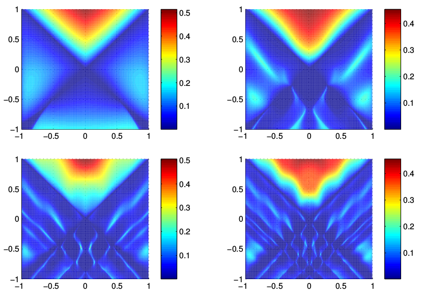
Results of the conductance calculation for two choices of parameters have been plotted as contour plots in Figs. 2 (a) and 2 (b). We discuss the features observed in the contour plots below.
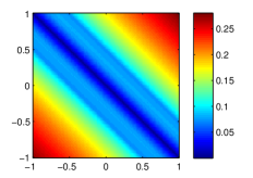
Zero Zeeman field : In Fig. 2 (a), a dominant feature is two dark-thick lines that appear along the diagonals: . These correspond to one of the two electron Fermi surfaces participating in Andreev reflection at having zero circumference. The lines correspond to crossover from retro- to specular- Andreev reflection. Another feature is that there are two islands of light-blue color around . This corresponds to specular Andreev reflection since the two electrons participating in the Andreev reflection come from above and below the CNP. All the data-points in the region correspond to specular Andreev reflection. Similarly, all the data points in the region correspond to retro Andreev reflection. We also notice an asymmetry in , which is due to a finite . These results and the discussion agree with that in Ref. efet16-prb .
Nonzero Zeeman field :
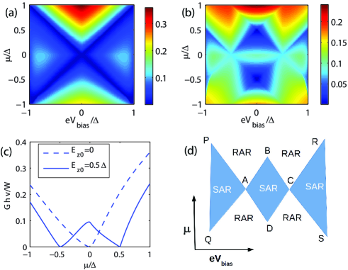
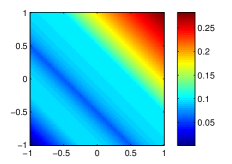
In Fig. 2 (b), the Zeeman field in the normal metal region is chosen to be . The striking features of this contour plot are: (i) three light blue islands, two of which are located around and one located around , and (ii) two dark blue patches located around .
To understand the features of Fig. 2 (b), let us define different points on the contour plot: , , , , , , and [each of these points is written in the form ]. Now, within the diamond , both the electrons contributing to Andreev reflection lie on different sides of the charge neutrality point. So, Andreev reflection is specular within this diamond. Also, in the triangles and the two electrons contributing to Andreev reflection lie on different sides of the CNP. Hence, Andreev reflection is specular in these regions. Outside of the two triangles and the diamond, the two electrons contributing to Andreev reflection lie on the same side of the charge neutrality point. Hence, in these regions, Andreev reflection is retro. In each of the two dark blue patches around the points and the data points are in proximity to CNP for both the electrons participating in the Andreev reflection. Since the size of the Fermi surface approaches zero as one tends to the CNP, the conductance is suppressed around points and . In contrast, along the lines , , , , , , and away from the points and , data points for only one of the two participating electrons (in Andreev reflection) is at the charge neutrality point.
More generally, for a given choice of , the diamond is formed by the points , , , and , and the points , , , and form the triangles and . Hence, in the case when , the diamond has zero area as can be seen in Fig. 2 (a). And the regions inside the two triangles and are described by the inequalities and , respectively. These are the regions where the Andreev reflection is specular. Outside these regions, the Andreev reflection is retro.
Zero bias cuts of Figs. 2(a) and 2(b) have been plotted in Fig. 2 (c). These clearly show that around the CNP, the zero-bias conductance is enhanced under an applied Zeeman field, while in the case of zero Zeeman field, the zero bias conductance is suppressed.
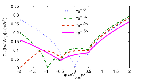
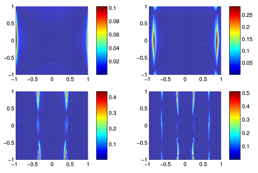
Choice of the parameter : Previously, we chose so as to allow for significant conductance despite accounting for a work function mismatch [modeled by the step function ]. Now, we examine the features of the conductance spectrum for different choices of and make a connection to previous works.
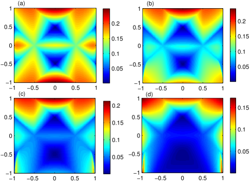
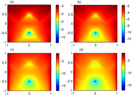
The step height essentially captures the junction transparency. For larger magnitudes of , the junction is less transparent and has a high resistance. We can see from Fig. 3 that for larger values of , the features of crossover from retro- to specular- Andreev reflection discussed earlier get blurred. From the works of Efetov et al. efet16 ; efet16-prb , we note that when NbSe2 is used as the superconductor on top of the BLG, the parameters are =5 meV and =1.2 meV. This closely corresponds to Fig. 3 (d) and we see that the features of the crossover from retro- to specular- Andreev reflection begin to vanish for the value of . To see the features for higher values of , we plot the conductance on a logarithmic scale in Fig.4. We see that the features discussed earlier vanish smoothly over the values of , and , except for two dips at . However, the dips correspond to orders of magnitude smaller conductance. Thus, we find that a transparent junction is very crucial to observing the features of crossover from retro- to specular- Andreev reflection.
IV Comparative analysis of the results replacing the superconductor with normal metal
In this section, we discuss the results of the system, where superconductivity in the system is absent, and make comparison to the results with the system containing superconductivity. We denote the part of the system having a nonzero Zeeman field by F (ferromagnet), and N refers to the normal metal part which has no Zeeman field. for all in the NF junction. The calculation for the NF junction is presented in Appendix A. As can be seen from the calculations, the bias and the chemical potential enter the equations as . Hence, the conductance depends only on the linear combination in the contour plot which is apparent in Fig. 5.
In Fig. 6, the conductance is plotted as a function of , for different values of step height . For , the conductance goes to zero at , since the size of the Fermi surface on the normal metal side goes to zero, and there are no momentum modes to carry the current. For finite values of , the situation changes since at , the Fermi surface has a finite size, and the current can flow from the F-side to the N-side. The asymmetry around is because of a finite value of .
Now, we turn to the comparison of conductances of different systems (NN, NF, SN, and SF) for a given choice of and other parameters. For (Fig. 7, top), all the curves are symmetric, while for the curves are not symmetric (except for SN and SF). For SF, the minima at and maximum at are due to the dispersions displaced due to Zeeman fields. This bump is where the specular Andreev reflection is enhanced by the Zeeman field. For NN, NF, and SN in the case , the conductance is zero at , which is due to zero size of the Fermi surface of the N region. When , (see Fig. 7, bottom) the size of Fermi surface is nonzero in the N region to the left in the NN and NF configurations, and there is a finite conductance even at for the NF configuration.
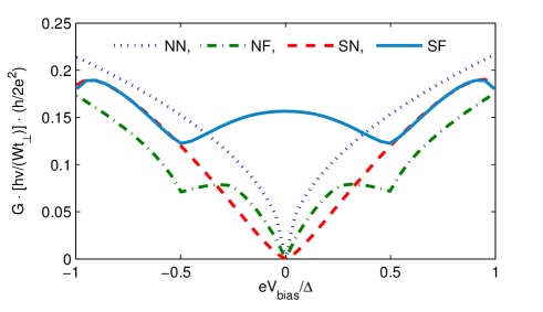
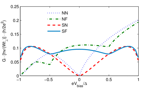
Now, we compare different curves in the bottom panel of Fig. 7. For NN and SN configurations, the N-region for has zero sized Fermi surface at zero bias. Hence the conductance at zero bias is zero (despite a nonzero sized Fermi surface in the region for NN). Now, when we turn to the case of NF, the Fermi surfaces on both sides of the junction at have nonzero size. Hence, the conductance is finite around . The conductance for NF approaches zero as since the size of Fermi surface approaches zero on the N-side of the junction as we have chosen . For the case of SF, the conductance is nonzero in the entire range shown since the size of the Fermi surface on F-side is always nonzero due to a finite value of the Zeeman field (), and on the S-side there is superconducting gap which favors Andreev reflection. Finally, the conductances in the lower panel are smaller than those in the upper panel since the step height is zero in the upper panel and is in the lower panel, reducing the transparency of the junctions studied in the lower panel.
V Experimental relevance
To implement our scheme experimentally, it is important to apply a Zeeman field in the NM part of the junction. An in-plane magnetic field which is less than the critical field to kill the superconductivity of the SC part in the system will achieve this. Another way to implement a Zeeman field is to bring a ferromagnetic insulator in proximity to the NM-side of the junction. It has been shown that ferromagnetism can be induced in graphene by such proximity coupling with several materials such as EuO, YIG and EuS haugen08 ; wang15 ; wei16 .
A typical sample will have a disorder which manifests as Fermi energy broadening . This means that the BLG sample must be of a sufficiently high quality so that the Fermi energy broadening is small (). Furthermore, observing the features of crossover for a fixed bias as is varied is important as the quasiparticle contribution to transport is the least in this regime. In addition, a finite temperature will result in thermal broadening and hence, performing the experiment at a low temperature is necessary to observe the features discussed here. The temperature has to be low compared to both the superconducting gap ( in NbSe2 efet16 ) and Zeeman energy (). Experimentally, reaching temperatures of about is possible and hence temperature does not pose a hindrance to implementing our scheme in realistic systems.
In a realistic system, the work function mismatch between the NM and SC regions can result in the formation of a NM region having a length-scale at the interface as discussed in Ref. tanake17 . Also, from the value of the work functions of NbSe2 and BLG, the step height is chosen to be in Ref. tanake17 in contrast to the limit in Ref. efet16 ; efet16-prb where the value of is chosen to match the experimental results. Our calculations combined with the choice of in Ref. efet16 ; efet16-prb point to a small value of () in contrast to the assertion made in Ref. tanake17 . This means that the effects of a p-n junction formed at the NM-SC interface may be negligible. In Appendix B, we study the effect of having a finite and show that it can be negligible.
VI Summary and conclusion
We have studied Andreev reflection at a junction of bilayer graphene and a superconductor. Since our main objective has been to observe the enhanced signatures of specular Andreev reflection, we introduce a Zeeman field and study the features on a contour plot of conductance versus chemical potential and bias voltage when these two energy scales are less than the superconducting gap. We find that a finite Zeeman field produces a diamond shaped region at the center where the Andreev reflection is purely specular. Furthermore, the lines bordering the diamond shaped region and two patches around the low bias region at the corners of the diamond show a low conductance, where the crossover from specular- to retro- type Andreev reflection occurs. Importantly, we find that for a barrier step-height that is of the same order of magnitude as the superconducting gap, the features of the crossover from retro- to specular- Andreev reflection are observable and for a barrier step-height much larger than the superconducting gap, the features vanish except for small regions of low conductance at . We have also analyzed the relative contributions from normal state conductance, where the superconductivity is switched off. Furthermore, we have discussed how our calculations can be tested in an experimental system.
Acknowledgements.
AD thanks Nanomission, Department of Science and Technology (DST) for the financial support under grants - DSTO1470 and DSTO1597. AS thanks DST Nanomission (DSTO1597) for funding. SM thanks the Indo-Israeli UGC-ISF project for funding.Appendix A
In this section, we give details of the calculation for the system comprising of a Zeeman field induced ferromagnetic region in contact with the normal metal region. This is simply the limit of the NM-SC junction described by Eq. (3) where for all . The wavefunction for an electron incident on the junction from onto , with energy has the form , where
| (7) | |||||
Here, , , ( is the angle of incidence so that the normal incidence corresponds to ),
Now, using the boundary condition, which is continuity of the wavefunction at , one can determine the scattering amplitudes , , , and . With this, the wavefunction is determined and using a formula similar to Eq. (LABEL:eq-conductance), the conductance can be calculated.
Appendix B
In this part, we study the effect of having a finite region of length on the NM part of the junction where . The Hamiltonian has the same form as in Eq. (3), except for two changes: and , where is a Heavyside step function. The wavefunction for an electron at energy (in the range: ) and spin ( is the eigenvalue of the operator ), incident from the NM side onto the SC has the form , such that
| (9) | |||||
where and are the electron- and hole- sector eigenspinors of the Hamiltonian on the NM side [given by Eq. (2)] with -component of momentum , and is the eigenspinor on the SC side with -component of momentum . Furthermore, the -component of electron and hole momenta on the NM side are given by:
| (10) |
where , , and . The continuity of at and in total give 16 equations for 16 scattering amplitudes to be solved. Then, the conductance is calculated using Eq. (LABEL:eq-conductance).
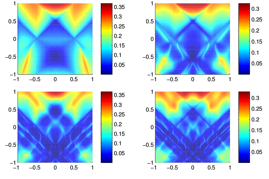
First, the conductance is calculated for , for various values of and a fixed value of in Fig. 8. It can be seen that for higher values of , Fabry-Pérot type oscillations soori12 are observed in the conductance spectra. Comparing this with the experimental results in Ref. efet16 , the absence of conductance oscillations there suggests that in a realistic system, is small ().
Next, we study the case of (discussed in Ref. tanake17 ) keeping in Fig. 9 for different values of . We see that for larger values of (), there are Fabry-Pérot type oscillations in conductance. Comparing these with the experimental results in Ref. efet16 , we see that must be small (). While the precise values of and are unknown in a realistic system, our results suggest that and . Furthermore, this limit of and is important to observe the features of the crossover from retro to specular Andreev reflection in a system with finite .
Now, we turn to the case of . In Fig. 10, we see how the conductance spectrum changes as is changed keeping fixed. The features of crossover still remain, but there are oscillations in the conductance spectrum due to Fabry-Pérot type interference, which occur due to modes in the region . The two dark regions of low conductance around the points and , and the dark lines and remain. Furthermore, the dark lines and remain, while the dark lines along and vanish. It is not possible to distinguish the Fabry-Pérot oscillations in the conductance spectrum from the crossover from specular to retro Andreev reflection, but with a knowledge of and the points: and in the conductance spectrum can be identified, thereby finding the crossover lines.
References
- (1)
- (2) A. F. Andreev, “The Thermal Conductivity of the Intermediate State in Superconductors”, J. Exp. Theor. Phys. 19, 1228 (1964).
- (3) G. E. Blonder, M. Tinkham, and T. M. Klapwijk, “Transition from metallic to tunneling regimes in superconducting microconstrictions: Excess current, charge imbalance, and supercurrent conversion”, Phys. Rev. B 25, 4515 (1982).
- (4) A. Kastalsky, A. W. Kleinsasser, L. H. Greene, R. Bhat, F. P. Milliken, and J. P. Harbison, “Observation of pair currents in superconductor-semiconductor contacts”, Phys. Rev. Lett. 67, 3026 (1991).
- (5) K. S. Novoselov, A.K. Geim, S.V. Morozov, D. Jiang, Y. Zhang, S.V. Dubonos, I.V. Grigorieva, and A.A. Firsov, “Electric Field Effect in Atomically Thin Carbon Films”, Science 306, 666 (2004).
- (6) A. H. Castro Neto, F. Guinea, N. M. R. Peres, K. S. Novoselov, and A. K. Geim, “The electronic properties of graphene”, Rev. Mod. Phys. 81, 109 (2009).
- (7) A. V. Rozhkov, A. O. Sboychakov, A. L. Rakhmanov, F. Nori, “Electronic properties of graphene-based bilayer systems”, Physics Reports 648, 1-104 (2016).
- (8) E McCann and M Koshino, “The electronic properties of bilayer graphene”, Rep. Prog. Phys. 76, 056503 (2013).
- (9) S. Bhattacharjee and K. Sengupta, “Tunneling Conductance of Graphene NIS Junctions”, Phys. Rev. Lett. 97, 217001 (2006).
- (10) C. W. J. Beenakker, “Specular Andreev Reflection in Graphene”, Phys. Rev. Lett. 97, 067007 (2006).
- (11) C. Benjamin and J. K. Pachos, “Detecting entangled states in graphene via crossed Andreev reflection”, Phys. Rev. B 78, 235403 (2008).
- (12) L. Majidi, and M. Zareyan, “Enhanced Andreev reflection in gapped graphene ”, Phys. Rev. B 86, 075443 (2012).
- (13) D. Rainis, F. Taddei, F. Dolcini, M. Polini, and R. Fazio, “Andreev reflection in graphene nanoribbons”, Phys. Rev. B 79, 115131 (2009).
- (14) M. R. Sahu, P. Raychaudhuri, and A. Das, “Andreev reflection near the Dirac point at Graphene - NbSe2 junction”, Phys. Rev. B 94, 235451 (2016).
- (15) D. K. Efetov , L. Wang, C. Handschin, K. B. Efetov, J. Shuang, R. Cava, T. Taniguchi, K. Watanabe, J. Hone, C. R. Dean and P. Kim, “Specular interband Andreev reflections at van der Waals interfaces between graphene and NbSe2”, Nat. Phys. 12, 328 (2016).
- (16) D. K. Efetov and K. B. Efetov, “Cross-over from retro to specular Andreev reflections in bilayer graphene”, Phys. Rev. B 94, 075403 (2016).
- (17) T. Ludwig, “Andreev reflection in bilayer graphene”, Phys. Rev. B 75, 195322 (2007).
- (18) R. Landauer, “ Spatial Variation of Currents and Fields Due to Localized Scatterers in Metallic Conduction” IBM J. Res. Dev. 1, 223 (1957); R. Landauer, “Electrical resistance of disordered one-dimensional lattices”, Philos. Mag. 21, 863 (1970); M. Büttiker, Y. Imry, R. Landauer, and S. Pinhas, “Generalized many-channel conductance formula with application to small rings”, Phys. Rev. B 31, 6207 (1985); M. Büttiker, “Four-Terminal Phase-Coherent Conductance”, Phys. Rev. Lett. 57, 1761 (1986); S. Datta, Electronic Transport in Mesoscopic Systems (Cambridge University Press, Cambridge, 1995).
- (19) A. Soori, S. Das and S. Rao, “Magnetic field induced Fabry- Pérot resonances in helical edge states”, Phys. Rev. B 86, 125312 (2012).
- (20) H. Haugen, D. Huertas-Hernando, and A. Brataas, “Spin transport in proximity-induced ferromagnetic graphene”, Phys. Rev. B 77, 115406 (2008).
- (21) Z. Wang, C. Tang, R. Sachs, Y. Barlas, and J. Shi, “Proximity-Induced Ferromagnetism in Graphene Revealed by the Anomalous Hall Effect”, Phys. Rev. Lett. 114, 016603 (2015).
- (22) P. Wei, S. Lee, F. Lemaitre, L. Pinel, D. Cutaia, W. Cha, F. Katmis, Y. Zhu, D. Heiman, J. Hone, J. S. Moodera and C.-T. Chen, “Strong interfacial exchange field in the graphene/EuS heterostructure”, Nat. Mater. 15, 711-716 (2016).
- (23) Y. Takane, K. Yarimizu, and A. Kanda, “Andreev Reflection in a Bilayer Graphene Junction: Role of Spatial Variation of the Charge Neutrality Point”, J. Phys. Soc. Jpn. 86, 064707 (2017).