Auto-Generation of Pipelined Hardware Designs for Polar Encoder
Abstract
This paper presents a general framework for auto-generation of pipelined polar encoder architectures. The proposed framework could be well represented by a general formula. Given arbitrary code length and the level of parallelism , the formula could specify the corresponding hardware architecture. We have written a compiler which could read the formula and then automatically generate its register-transfer level (RTL) description suitable for FPGA or ASIC implementation. With this hardware generation system, one could explore the design space and make a trade-off between cost and performance. Our experimental results have demonstrated the efficiency of this auto-generator for polar encoder architectures.
Index Terms:
Polar encoder, pipelined architecture, hardware auto-generation, high-level synthesis.I Introduction
Polar code [1], the first channel code which can provably achieve the capacity of the binary-input discrete memoryless channels (BDMCs), has been considered as the recent breakthrough of coding theory. Recently, polar code has been adopted by the enhanced mobile broadband (eMBB) control channels for the G NR interface. As pointed out by [1], to achieve a good error-correcting performance of polar code, the code length is expected to be sufficiently long. However, as for polar code, the hardware complexity of fully parallel encoder will be high as the code length increases. Therefore, pipelined architecture should be introduced to reduce the hardware cost. Using folding transformation [2], [3] has proposed both feed-forward and feed-back polar encoder with -parallel processing; [4] has proposed pipelined polar encoder architecture with -parallel processing. Although [4] has claimed that the folding transformation could derive polar encoder with any level of parallelism, the detailed framework is not given.
In synthesizing hardware architectures for an -bit polar encoder, different level of parallelism leads to different latency, throughput, silicon area and memory cost. Intuitively, the level of parallelism suitable for an -bit polar encoder should be , where is a power of two. Thus, as the code length increases, there will be more choices of and the design space will be wider. Therefore, it will be exhausting to choose the optimal values of and under different hardware constraints.
In order to fulfill the requirements of different applications, a auto-generator which can connivently output polar encoder architecture with given code length and parallelism is highly expected. Also, this auto-generator can free the hardware designers from the laborious case designs, bypass the hardware details, and give the design space in a more convenient way. Inspired by a fast Fourier transform (FFT) generator [5] which could automatically generate FFT hardware architecture with arbitrary parallelism and figure out hardware cost, this paper proposes an auto-generation system which could produce polar encoder hardware architecture with arbitrary code length and arbitrary level of parallelism.
The remainder of this paper is organized as follows. In Section II, the brief description of polar encoding is introduced. In Section III, we propose the generation system of polar encoder and an exemplary -bit polar encoder with -parallel processing. In Section IV, the analysis of the performance of the generation system is given. In Section V, we conclude and remark on the entire paper.
II Preliminaries
II-A Polar Encoder
In polar code encoding, is regarded as the source word and as the codeword. The encoding scheme can be defined by Eq. , where and are the generation matrix and the bit-reversal permutation matrix respectively, and is the Kronecker power of with and .
| (1) |
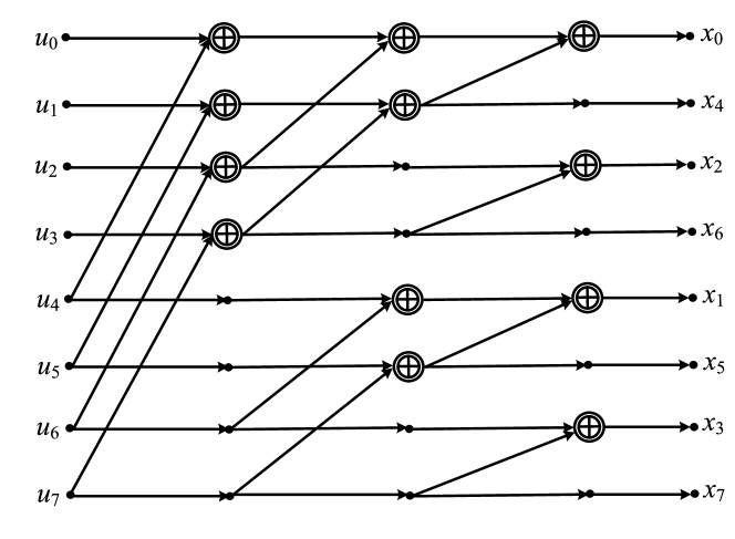
As proved by [3], the data-flow graph (DGF) of polar encoder could be derived from the DFG of FFT processors by replacing all the butterfly modules with xor-and-pass modules, and all the twiddle factors with 1’s. Therefore, the proposed framework for polar encoder has the potential for implementing the pipelined hardware architecture for FFT by reversing the replacement. An exemplary DGF of an -bit polar encoder is shown in Fig. 1. Note that this DFG is similar to the that of an -point radix- decimation-in-frequency (DIF) FFT processor in the way mentioned above.
III Hardware Generation
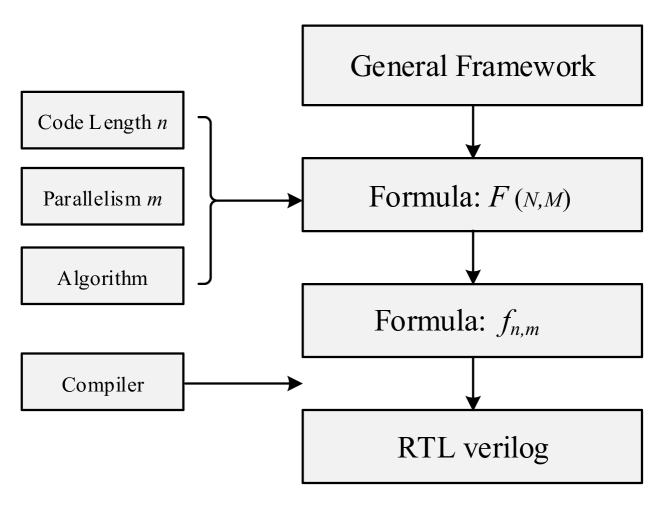
In this section, we introduce the general pipelined framework for polar encoder with arbitrary code length and arbitrary level of parallelism . The general framework could be easily denoted by a general formula . Then we show how to use an algorithm to derive a specific formula from based on the values of and . Finally, a compiler is employed to translate into RTL description. The hardware generation system is illustrated in Fig. 2.
III-A From General Framework to Formula
Consider that the general framework is expected to implement polar encoder with arbitrary code length and arbitrary level of parallelism, the framework should be scalable, i.e., the number of stages and the number of hardware modules in each stage should change with the values of and . Such a scalable framework could represented by formula shown in Eq. . Here the parameters and are powers of , and . Before we go into details of , we introduce all the symbols that might be used in and , as well as the symbols’ corresponding hardware modules. Note that the final hardware implementation of is the serial connection of the individual modules of different symbols. Fig. 3 illustrates all the exemplary modules, as well as symbols, that might be used in our design, all of which take as input and as output.
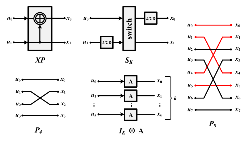
Symbol XP represents an xor-and-pass module that achieves: (in GF()) and The number of inputs of XP is fixed and equals to in our design.
Symbol ( is a power of , ) represents a switch with delay elements (denoted by ) on each side. A -bit counter is needed to control the switch: the value of the most significant bit of the counter infers direct data transfer, and the value infers cross data transfer. The number of inputs of is fixed and equals to .
Symbol ( is a power of , ) denotes the permutation on an -dimensional vector. The detail function of is illustrated in Algorithm 1. Intuitively, is the duplication of . For example, could be viewed as partial overlap of two modules with red wires and black wires respectively.
Symbol ) ( is a power of , ) is a Kronecker product representing parallel instances of module , where is an abstract module and could be replaced by XP, or . Note that when , equals to . Suppose that has inputs, the number of inputs of ) equals .
The general formula is composed of symbols mentioned above, except that the in Eq. is a variable module. When deriving from , symbol should be replaced by or according to its subscript. In Algorithm 2, as the code length and the level of parallelism are given, all the subscripts of each symbol in will be figure out. Then the module is replaced by or based on the value of the subscript of . Finally, the formula is determined.
III-B Compiler
We have built a compiler in Python that takes as input and automatically connects all the basic modules in in left-to-right order. Specifically, as we input and into , the will be determined and transformed into the register-transfer level (RTL) Verilog by the compiler. The detail of the compiler is beyond the scope of this paper; we only provide a brief introduction here.
There are totally three types of basic modules in the formula : the xor-and-pass module XP, the switch module , and the permutation module . There are two ways to expand these modules. The first one is to employ the symbol to layout the duplication of one module in a parallel way. The other one is to change the symbols’ subscripts. Therefore, the compiler needs to read each symbol of from left to right, and recognizes as well as each symbol’s subscript. Then the compiler could determine the specific hardware architecture and print the Verilog files.
III-C Input and Output Orders
The input and output data of this framework are in regular order. Suppose the input data of is , since represents a pipelined architecture, will be divided into -dimensional vectors illustrated in Eq. , where . All the data in will be entered into the encoder in parallel, and indicates the sequence of the input vector, i.e., is the first set of the input data and the is the last set of the input data. The output data are in bit-reversal order. Specifically, suppose is the theoretical codeword and is in the bit-reversal form of . Then the -th output vector equals to , where .
| (3) |
For the general framework, the processing latency (clock cycles) is . The number of xor gates and delay elements are:
| (4) |
III-D A 32-Bit 8-Parallel Polar Encoder
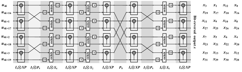
According to Algorithm 2, given and , formulas and are obtained in Eq. and Eq. , respectively. The hardware architecture is illustrated in Fig. 4, which consists of xor gates and delay elements in accordance with Eq. . The architecture could be split in columns, each of which has its relevant symbol under the column. Note that Eq. is actually composed of all the symbols at the bottom of Fig. 4. The order of the input data () at the leftmost part of Fig. 4 conforms to the order mentioned above. The output data is in the bit-reversal order.
IV Performance and Complexity
Some of the hardware designs derived from the auto-generation system were implemented on the Xilinx Virtex-7 VC709 FPGA platform with Virtex-7 XC7VX690T. All the design examples are of the same code length , but with different level of parallelism. The synthesis results are illustrated in Table I. From the table, it can be observed that the throughput (T/P) and the number of Slice LUTs and Slice Registers increase as the value of increases. In an extreme case, the polar encoder with consumes more Slice LUTs than the polar encoder with by but achieves higher throughput by .
As mentioned in Section III, the value of conforms to . Then, given the code length , the generation system could implement designs with different , covering a wide cost/performance trade-off space. Therefore, one could choose the most suitable polar encoder in the design space to fit the application.
| Slice LUTs | Slice Registers | Max freq | T/P | ||
| (MHz) | (Gbps) | ||||
V Conclusion
This paper proposes an auto-generation system for the hardware architecture of polar encoder. The system could offer users a wide range of design space so that the users could make a trade-off between cost and performance to best fit their applications. The essence of the generation system lies in the formula-based expression of the general framework for polar encoder that could achieve encoding with arbitrary code length and arbitrary parallelism. This auto-generation can help designers to conveniently design polar encoder without touching hardware details. The derivation of design space can further help us to identify the required design.
In this paper, we also introduce the scalable hardware modules associated with the formula, as well as the compiler that could transform the formula into RTL Verilog files. Synthesis results on FPGA have demonstrated the efficiency and the large trade-off space of the auto-generated circuits.
References
- [1] E. Arikan, “Channel polarization: A method for constructing capacity-achieving codes for symmetric binary-input memoryless channels,” IEEE Transactions on Information Theory, vol. 55, no. 7, pp. 3051–3073, 2009.
- [2] K. K. Parhi, C.-Y. Wang, and A. P. Brown, “Synthesis of control circuits in folded pipelined dsp architectures,” IEEE Journal of Solid-State Circuits, vol. 27, no. 1, pp. 29–43, 1992.
- [3] C. Zhang, J. Yang, X. You, and S. Xu, “Pipelined implementations of polar encoder and feed-back part for SC polar decoder,” in IEEE International Symposium on Circuits and Systems (ISCAS), 2015, pp. 3032–3035.
- [4] H. Yoo and I.-C. Park, “Partially parallel encoder architecture for long polar codes,” IEEE Transactions on Circuits and Systems II: Express Briefs, vol. 62, no. 3, pp. 306–310, 2015.
- [5] P. Milder, F. Franchetti, J. C. Hoe, and M. Püschel, “Computer generation of hardware for linear digital signal processing transforms,” ACM Transactions on Design Automation of Electronic Systems (TODAES), vol. 17, no. 2, p. 15, 2012.
- [6] C. Zhang, B. Yuan, and K. K. Parhi, “Reduced-latency SC polar decoder architectures,” in Proc. IEEE International Conference on Communications (ICC), June 2012, pp. 3471–3475.
- [7] C. Zhang and K. Parhi, “Low-latency sequential and overlapped architectures for successive cancellation polar decoder,” IEEE Trans. Signal Process., vol. 61, no. 10, pp. 2429–2441, 2013.
- [8] J. Yang, C. Zhang, H. Zhou, and X. You, “Pipelined belief propagation polar decoders,” in Proc. IEEE International Symposium on Circuits and Systems (ISCAS), May 2016, pp. 413–416.