Gate-Tunable Quantum Dot in a High Quality Single Layer MoS2 Van der Waals Heterostructure
Abstract
We have fabricated an encapsulated monolayer MoS2 device with metallic ohmic contacts through a pre-patterned hBN layer. In the bulk, we observe an electron mobility as high as 3000 cm2/Vs at a density of 7 1012 cm-2 at a temperature of 1.7 K. Shubnikov-de Haas oscillations start at magnetic fields as low as 3.3 T. By realizing a single quantum dot gate structure on top of the hBN we are able to confine electrons in MoS2 and observe the Coulomb blockade effect. By tuning the middle gate voltage we reach a double dot regime where we observe the standard honeycomb pattern in the charge stability diagram.
Contrary to graphene, in monolayer molybdenum disulfide (MoS2) inversion symmetry is broken. This, together with the presence of time-reversal symmetry, endows single layer MoS2 with individually addressable valleys in momentum space at the K and K′ points in the first Brillouin zone. Xiao et al. (2012); Chhowalla et al. (2013); Xu et al. (2014); Kormányos et al. (2013) This valley addressability facilitates the momentum state of electrons to be used for novel qubit architectures. Recent theoretical works have been exploring the possibility of using spin and valley states of gate-defined quantum dots in 2D MoS2 as quantum bits. Kormányos et al. (2014); Novoselov et al. (2016); Loss and DiVincenzo (1998) In this manuscript, we describe the observation of Coulomb blockade in single and coupled dot in a high quality single layer MoS2. The high electronic quality of our monolayer MoS2 results in the observation of Shubnikov-de Haas oscillations (SdHO) occurring at magnetic fields as low as 3.3 T. The 2DEG in the MoS2 can be electrostatically depleted below the gate pattern with resistance values exceeding the resistance quantum h/e2 by orders of magnitude. We observe Coulomb blockade resonances close to pinch-off indicating single electron tunneling in and out of the dot. By adjusting the gate voltages, we are able to tune the electrostatic landscape inside the dot and to form a double dot system within a single dot gate structure. Zhang et al. (2017); Song et al. (2015); Wang et al. (2016); Epping et al. (2016)
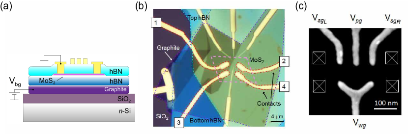
In Fig. 1(a), we show the schematic of a monolayer MoS2 ( 0.7 nm thick) encapsulated between two hexagonal boron nitride (hBN) layers. The measured MoS2 flake was exfoliated from natural bulk crystal (SPI supplies). The bottom hBN layer is 30 nm thick and works both as an atomically flat substrate and as a dielectric that isolates the MoS2 from a graphite backgate. The graphite gate enables us to control electrostatically the electron density in MoS2 with the voltage Vbg. The layers thicknesses were determined by atomic force microscopy (AFM). The top hBN layer (50nm thick) has been pre-patterned using E-beam lithography and reactive ion etching. Wang et al. (2015) This enables us to evaporate metallic contacts (Ti/Au) on top of the MoS2 layer where the hBN has been etched away, without exposing the channel region to organic residues remaining from the fabrication process. Allain et al. (2015) Prior to metal evaporation, the heterostructure has been annealed in forming gas (Ar/H2) at 300 for 30 minutes in order to remove most of the organic residues on top of the MoS2 contact regions and to achieve ohmic contact behavior. 5 nm of Ti and 65 nm of Au were deposited by means of electron-beam evaporation at a pressure of 210-8 mbar. This fabrication process enables us to realize ohmic contacts on monolayer MoS2 without the use of graphene or Co/h-BN electrodes as in previous works. Cui et al. (2017, 2015) Fig. 1(b) shows the optical micrograph of the device where the monolayer MoS2 is outlined in pink. The MoS2 crystal was exfoliated and the heterostructure assembled in an argon environment (H2O and O2 levels 0.1 ppm). Bretheau et al. (2017); Pisoni et al. (2017) The top hBN serves as a dielectric layer for the top gate structure. Fig. 1(c) displays the scanning electron microscope (SEM) image of the top gate structure in which the voltages applied to the gates are labeled VsgL, Vpg, VsgR and Vwg. To avoid electrostatic inhomogeneities, the gate structure has been deposited on a bubble-free region on top of the MoS2. The gate-defined lithographic dot radius is 70 nm.
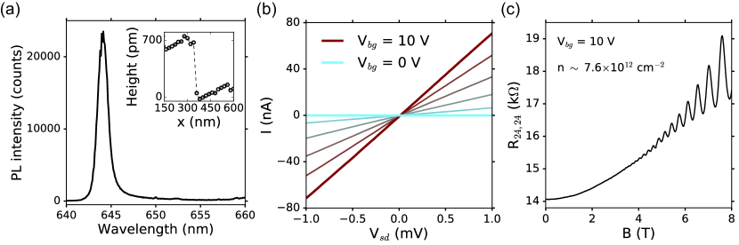
Fig. 2(a) displays the measured photoluminescence (PL) spectrum at 4 K and the AFM height signal (inset) of the MoS2 flake. The shown PL spectrum was measured at Vbg = -1 V, where the sample is devoid of free electrons. We note that the PL signal is slightly distorted on the shorter wavelength side because of the longpass filter used to suppress the excitation HeNe laser. The Full Width at Half Maximum (FWHM) of the exciton resonance is 4 meV and the peak is centered at a wavelength of 644 nm corresponding to 1.925 eV. For a few layer sample the PL spectrum consists of multiple emission peaks and lower PL intensity, we then conclude that our sample is a single layer MoS2. Mak et al. (2010) The AFM height signal shows a step height of 0.7 nm, in agreement with previous single layer MoS2 characterizations. Radisavljevic et al. (2011) Fig. 2(b) shows the low temperature (T 1.7 K) current (I) flowing through the device as a function of the voltage (Vsd) applied between two electrodes (2 and 4 in Fig. 1(b)) at various Vbg and zero voltage between patterned top gates and 2DEG. Linear I-Vsd curves are observed for Vbg1.5 V indicating ohmic contact behavior. The resistance decreases with increasing Vbg as expected for an n-type semiconductor. Cui et al. (2015) In order to estimate the quality of our device we performed magnetotransport measurements at T 1.7 K, using standard lock-in techniques at 80.31 Hz. Fig. 2(c) shows the resistance R24,24 as a function of magnetic field B, at the Hall density n 7.6 1012 cm-2. We observe the appearance of SdHO at B 3.3 T, yielding a lower limit for the mobility of 3000 cm2/Vs.
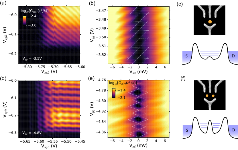
The 2DEG in the MoS2 can be locally depleted by applying negative voltages to the top gate structure. This structure allows us to confine electrons in a region of space small enough to observe the Coulomb blockade effect. Kouwenhoven, Austing, and Tarucha (2001) Fig. 3 displays the charge stability diagram and the transport spectroscopy of the quantum dot, at T 1.7 K and Vbg = 3.4 V. By varying Vpg we can modify the electrostatic potential landscape inside the dot and tune the coupling strength in order to observe both single and double dot regimes. Fig. 3(a, d) show the differential conductance on a logarithmic scale as a function of the left (VsgL) and right (VsgR) barrier gate voltages at Vpg = -3.5 V and -4.8 V respectively. When Vpg = -3.5 V, close to pinch off, we observe parallel resonances with intermittent Coulomb blockade for tunneling of electrons on and off the single dot (Fig. 3(c)). The lines are rather straight indicating that additional localized states possibly caused by disorder in MoS2 are of minor importance. The high quality of our monolayer MoS2 device yields a mean free path of 150 nm, slightly larger than the dot size. The measured conductance peaks exhibit a FWHM 5KBT as expected for thermally broadened peaks in the multilevel transport regime. Beenakker (1991) From the peaks spacing along the VsgL and VsgR axis in Fig. 3(a), we estimate the capacitance between the dot and the left and right barrier gates to be 6.7 aF and 5.9 aF respectively. Kouwenhoven, Austing, and Tarucha (2001) By tuning the gate voltage Vpg to more negative values, as shown in Fig. 3(d), we observe a hexagonal array of lines which is the signature for the formation of two coupled quantum dots (Fig. 3(f)). van der Wiel et al. (2002) According to the dimensions of the honeycomb pattern in Fig. 3(d), the capacitances between the dot and the left and right barrier gates can be determined to be 5.8 aF and 4.8 aF respectively and the cross-capacitances to be 0.5 aF. Fig. 3(b, e) display the differential conductance on a logarithmic scale as a function of the source-drain bias Vsd and Vpg. In the single dot regime (Fig. 3(b), we observe regular even-spaced Coulomb diamonds. From the height of the Coulomb diamonds along the Vsd axis, we estimate the charging energy to be 2 meV. By employing , Kouwenhoven, Austing, and Tarucha (2001) with = 4 the relative permittivity of hBN, Young et al. (2012) we estimate the radius of the dot to be 280 nm. The discrepancy between the estimated dot radius and the gate structure design can be assigned to the presence of the metallic gates and the adjacent source and drain leads that significantly affect the capacitance. Kouwenhoven, Austing, and Tarucha (2001) From the Coulomb blockade diamond measurements, we read the plunger gate lever arm 0.19 as the ratio between the charging energy and the peaks spacing along the Vpg axis. In the double dot regime (Fig. 3(e)), we observe the interchange of small and big Coulomb diamonds that, together with the honeycomb pattern in Fig. 3(d), may indicate the presence of two quantum dots. Kouwenhoven, Austing, and Tarucha (2001)
In conclusion, we have developed a fabrication technique, that allows us to realize ohmic contacts on monolayer MoS2 by employing metallic gates evaporated directly on top of the MoS2 surface instead of using graphene electrodes or Co/h-BN contacts, Cui et al. (2017, 2015) without affecting the electronic quality of the 2DEG. We observe the appearance of SdHO at lower magnetic field compared to previous work, Cui et al. (2015) indicating an electron mobility exceeding 3000 cm2/Vs. By electrostatically depleting the MoS2 2DEG we are able to confine electrons and observe Coulomb blockade effects in single and double dots. The samples are clean enough that the disorder-localized states do not affect the experimental observations. Gate-defined quantum dots formed in 2D semiconducting Transition Metal Dichalcogenides are the first step towards the realization of spin-valley qubits, filters and other intriguing valleytronic devices. Kormányos et al. (2014); Loss and DiVincenzo (1998); Brooks and Burkard (2017)
Acknowledgements.
The authors acknowledge financial support from the Graphene Flagship, the EU Spin-Nano RTN network, and the National Center of Competence in Research on Quantum Science and Technology (NCCR QSIT) funded by the Swiss National Science Foundation. Growth of hexagonal boron nitride crystals was supported by the Elemental Strategy Initiative conducted by the MEXT, Japan and JSPS KAKENHI Grant Numbers JP15K21722.References
- Xiao et al. (2012) D. Xiao, G.-B. Liu, W. Feng, X. Xu, and W. Yao, Physical Review Letters 108, 196802 (2012).
- Chhowalla et al. (2013) M. Chhowalla, H. S. Shin, G. Eda, L.-J. Li, K. P. Loh, and H. Zhang, Nature Chemistry 5, 263 (2013).
- Xu et al. (2014) X. Xu, W. Yao, D. Xiao, and T. F. Heinz, Nature Physics 10, 343 (2014).
- Kormányos et al. (2013) A. Kormányos, V. Zólyomi, N. D. Drummond, P. Rakyta, G. Burkard, and V. I. Fal’ko, Physical Review B 88, 045416 (2013).
- Kormányos et al. (2014) A. Kormányos, V. Zólyomi, N. D. Drummond, and G. Burkard, Physical Review X 4, 011034 (2014).
- Novoselov et al. (2016) K. S. Novoselov, A. Mishchenko, A. Carvalho, and A. H. C. Neto, Science 353, aac9439 (2016).
- Loss and DiVincenzo (1998) D. Loss and D. P. DiVincenzo, Physical Review A 57, 120 (1998).
- Zhang et al. (2017) Z.-Z. Zhang, X.-X. Song, G. Luo, G.-W. Deng, V. Mosallanejad, T. Taniguchi, K. Watanabe, H.-O. Li, G. Cao, G.-C. Guo, F. Nori, and G.-P. Guo, Science Advances 3, e1701699 (2017).
- Song et al. (2015) X.-X. Song, D. Liu, V. Mosallanejad, J. You, T.-Y. Han, D.-T. Chen, H.-O. Li, G. Cao, M. Xiao, G.-C. Guo, and G.-P. Guo, 7, 16867 (2015).
- Wang et al. (2016) K. Wang, T. Taniguchi, K. Watanabe, and P. Kim, arXiv:1610.02929 [cond-mat] (2016), arXiv: 1610.02929.
- Epping et al. (2016) A. Epping, L. Banszerus, J. Güttinger, L. Krückeberg, K. Watanabe, T. Taniguchi, F. Hassler, B. Beschoten, and C. Stampfer, arXiv:1612.01118 [cond-mat] (2016), arXiv: 1612.01118.
- Wang et al. (2015) J. I.-J. Wang, Y. Yang, Y.-A. Chen, K. Watanabe, T. Taniguchi, H. O. H. Churchill, and P. Jarillo-Herrero, Nano Letters 15, 1898 (2015).
- Allain et al. (2015) A. Allain, J. Kang, K. Banerjee, and A. Kis, Nature Materials 14, 1195 (2015).
- Cui et al. (2017) X. Cui, E.-M. Shih, L. A. Jauregui, S. H. Chae, Y. D. Kim, B. Li, D. Seo, K. Pistunova, J. Yin, J.-H. Park, H.-J. Choi, Y. H. Lee, K. Watanabe, T. Taniguchi, P. Kim, C. R. Dean, and J. C. Hone, Nano Letters 17, 4781 (2017).
- Cui et al. (2015) X. Cui, G.-H. Lee, Y. D. Kim, G. Arefe, P. Y. Huang, C.-H. Lee, D. A. Chenet, X. Zhang, L. Wang, F. Ye, F. Pizzocchero, B. S. Jessen, K. Watanabe, T. Taniguchi, D. A. Muller, T. Low, P. Kim, and J. Hone, Nature Nanotechnology 10, 534 (2015).
- Bretheau et al. (2017) L. Bretheau, J. I.-J. Wang, R. Pisoni, K. Watanabe, T. Taniguchi, and P. Jarillo-Herrero, Nature Physics advance online publication (2017), 10.1038/nphys4110.
- Pisoni et al. (2017) R. Pisoni, Y. Lee, H. Overweg, M. Eich, P. Simonet, K. Watanabe, T. Taniguchi, R. Gorbachev, T. Ihn, and K. Ensslin, Nano Letters 17, 5008 (2017).
- Mak et al. (2010) K. F. Mak, C. Lee, J. Hone, J. Shan, and T. F. Heinz, Physical Review Letters 105, 136805 (2010).
- Radisavljevic et al. (2011) B. Radisavljevic, A. Radenovic, J. Brivio, V. Giacometti, and A. Kis, Nature Nanotechnology 6, 147 (2011).
- Kouwenhoven, Austing, and Tarucha (2001) L. P. Kouwenhoven, D. G. Austing, and S. Tarucha, Reports on Progress in Physics 64, 701 (2001).
- Beenakker (1991) C. W. J. Beenakker, Physical Review B 44, 1646 (1991).
- van der Wiel et al. (2002) W. G. van der Wiel, S. De Franceschi, J. M. Elzerman, T. Fujisawa, S. Tarucha, and L. P. Kouwenhoven, Reviews of Modern Physics 75, 1 (2002).
- Young et al. (2012) A. F. Young, C. R. Dean, I. Meric, S. Sorgenfrei, H. Ren, K. Watanabe, T. Taniguchi, J. Hone, K. L. Shepard, and P. Kim, Physical Review B 85, 235458 (2012).
- Brooks and Burkard (2017) M. Brooks and G. Burkard, Physical Review B 95, 245411 (2017).