Now at ]LPEM, CNRS, ESPCI Paris, PSL Research University, UPMC, Paris, France
Sample-based calibration for cryogenic broadband microwave reflectometry measurements
Abstract
The characteristic frequencies of a system provide important information on the phenomena that govern its physical properties. In this framework, there has recently been renewed interest in cryogenic microwave characterization for condensed matter systems since it allows to probe energy scales of the order of a few eV. However, broadband measurements of the absolute value of a sample response in this frequency range are extremely sensitive to its environment and require a careful calibration. In this paper, we present an in situ calibration method for cryogenic broadband microwave reflectometry experiments that is both simple to implement and through which the effect of the sample electromagnetic environment can be minimized. The calibration references are here provided by the sample itself, at three reference temperatures where its impedance is assumed or measured, and not by external standards as is usual. We compare the frequency-dependent complex impedance (0.1–2 GHz) of an a-Nb15Si85 superconducting thin film obtained through this Sample-Based Calibration (SBC) and through an Open-Short-Load Standard Calibration (SC) when working at very low temperature (0.02–4 K) and show that the SBC allows us to obtain the absolute response of the sample. This method brings the calibration planes as close as possible to the sample, so that the environment electrodynamic response does not affect the measurement, provided it is temperature independent. This results in a heightened sensitivity, for a given experimental set–up.
pacs:
73.50.-h, 74.25.fc, 74.25.nn, 74.62.En, 74.1.BdI Introduction
Measuring the frequency-dependent response of a system has long been a powerful mean to characterize it by determining its natural frequencies. Recently, there has been a surge in interest for microwave characterization of condensed matter systems. Indeed, microwave technology has evolved and now enables very sensitive measurements down to temperatures below 1 K. Condensed matter properties in the eV energy range can therefore be investigated Scheffler and Dressel (2005); Armitage (2009); Dressel (2013) through this technique. One can for instance probe the intrinsic dynamics of conductors Gabelli et al. (2006, 2007) or design new measurement set-ups to determine the electrodynamic response of systems in the quantum regime, when (where and are the Planck and Boltzmann constants respectively, is the probe frequency and the temperature), as has recently attracted much attention Sachdev (1999). However, these measurements still remain challenging due to the combination of high frequency and low temperature.
Microwave measurements can be performed using resonant cavities Hafner et al. (2014); Chen et al. (2004). The sample of interest is then inserted within the set-up and one observes how the frequency response evolves. These techniques present a high sensitivity and do not require any external calibration. There has recently been tremendous experimental progress in this field, through the development of very high quality factor superconducting resonators Kubo et al. (2011); Dassonneville et al. (2013). However, they only work at selected frequencies corresponding to high order eigenmodes of a resonator and are mainly suitable for systems which impedance does not exhibit large variations in the considered frequency range. They also add uncontrolled parameters due to the coupling between the sample and the resonator. Broadband measurements, on the other hand, provide richer information on the system dynamical response, but are extremely sensitive to the set-up calibration. Indeed, when a microwave is sent towards a sample, the reflected or transmitted signal depends on the sample impedance , the quantity of interest, but also on the set-up itself. This constraint is easily overcome when working at room temperature where three so-called “Standards” can be measured before determining the sample’s response. For this purpose, one usually uses an open circuit (O), a short circuit (S) and a load (L) matching the characteristic impedance of the microwave measurement setup 50 . At low temperature, however, calibrating the set-up becomes more complex: temperature significantly influences physical characteristics of materials such as their impedance, dielectric constant or thermal contraction and hence changes their microwave characteristics.
Several methods have been proposed to solve this long-standing issue. Some have successively cooled down three standards at low temperature before measuring the sampleReuss (2000); Kitano et al. (2008); Stutzman et al. (2000); Steinberg et al. (2012); Scheffler et al. (2015). In the following, this will be referred to as the “Standard Calibration” (SC). Others considered the room-temperature calibration to be valid for two standards and used the sample at low temperature, either in the superconducting state or in a resistive state, as the third referenceBooth et al. (1994); Kitano et al. (2008); Silva et al. (2016); Sarti et al. (2005). The main drawback of both methods relies in the fact that the various cool-downs are not performed in perfectly identical conditions. In particular, they do not fully take into account the systematic errors induced by thermal gradients, which result in errors in the determination of the sample impedance. Moreover, the second procedure assumes that the sample impedance is known at one temperature. More recently, translatable microwave probes Meschede et al. (1992); Orloff et al. (2011) and electromechanical switches have been used to measure the standards and the sample at low temperature, during a single cool-downCano and Artal (2009); Yeh and Anlage (2013); Ranzani et al. (2013). However, translatable probes are difficult to implement at very low temperatures ( 1 K) and switches often contain magnetic parts that render them unsuitable for applications under magnetic field. In addition, these methods are sensitive to set-up imperfections: the transmission lines going to the standards and to the sample may for instance be slightly different. The sample itself is often composed of the material of interest connected to the set-up via a waveguide which response will be included in the measurement.
In this paper, we present an alternative calibration method for broadband microwave reflectometry measurements. This calibration is performed in situ and at low temperature and requires a sample with a parameter-dependent impedance (whether temperature, magnetic field, pressureLimelette et al. (2003), DC current, …). The method is then based on the knowledge of the sample impedance at three different values of this parameter and allows to define the calibration plane for the measurement as close as possible to the sample. In the following, it will be referred to as the “Sample-Based Calibration” (SBC).
In section II, we will detail our experimental setup. Section III will outline the general principle of the calibration. We apply it to a superconducting sample, described in section IV, which varying impedance provides a good testing ground for any calibration method. We will finally compare in section VI the results obtained by the SC, detailed in section V, to those provided by the SBC.
II Experimental setup
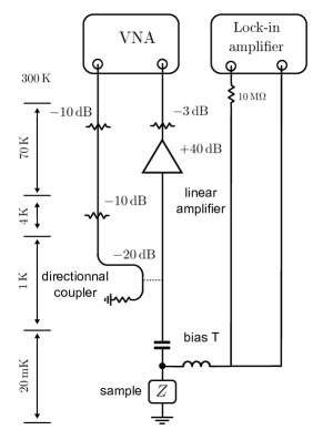
We performed broadband microwave reflectometry measurements down to very low temperatures (T 20 mK) in a cryogen-free dilution refrigerator. The measurement setup is schematically shown in Fig. 1. Cryogenic measurements require a low excitation power to ensure thermal equilibrium between the sample and the thermal bath, resulting in a small reflected signal by the sample. Successive attenuations of the incoming signal are thus needed at the different stages of the refrigerator to minimize the thermal noise arriving on the sample, while the sample’s reflection has to be subsequently amplified. These two conditions are met by using a directional coupler at K, which allows us to decouple the excitation and detection microwave lines. The microwave power is delivered by a Rohde Schwarz ZVB Vector Network Analyzer (VNA), which also measures the reflected signal . The bandwidth of this setup is set at low frequency, = 100 MHz, by the cryogenic HEMT amplifier (Miteq AFS4-00100800-22-CR-4, noise temperature 70 K Gabelli and Reulet (2008)), while the upper frequency limit, = 2 GHz, is fixed by the directional coupler (Mini-circuit ZFDC-20-5+).
A low-frequency ( 77 Hz) bias is simultaneously applied to the sample by a lock-in amplifier through a bias tee to measure the sample low frequency resistance. Measurements are performed in the linear regime where both the microwave power ( fW on the sample) and the lock-in amplifier current ( 1 A) are sufficiently low to prevent heating the sample.
III Calibration Principle
In broadband reflectometry, the attenuation of microwave lines is temperature-dependent and the set-up therefore requires a calibration to relate the measured reflected signal to the signal actually reflected by the sample only Kitano et al. (2008); Booth et al. (1994). Indeed, the cables as well as the various interfaces between connectors modify the amplitude and the phase of the propagating signal. The point of any calibration method is to characterize these extrinsic effects.
The reflectometry set-up depicted Fig. 1 can be modeled by a three-ports system, as shown in Fig. 2. Ports #1 and #2 correspond to the source and the detector of the VNA, respectively, while the sample is connected to port #3, generally through a sample holder. At each port i, the incoming and outgoing waves amplitudes are labeled and , respectively. These complex waves are related through four calibration coefficients: and describe the transmission of the excitation and detection lines respectively; represents the parasitic coupling between the excitation and detection lines due to the imperfections of the directional coupler insulation; whereas corresponds to part of the signal being reflected back to port #3, originating from the impedance mismatch of the microwave line connected to the sample.
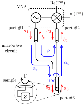
The reflection coefficient, , measured at the VNA, is then related to the reflection at port #3, by :
| (1) |
Note that reflects the attenuation of the entire line. Moreover, if is the complex impedance of the elements between port #3 and the ground, one has:
| (2) |
From equation (1), it is clear that three independent complex coefficients (, , ) are needed in order to retrieve from the measurement of . Let us emphasize that these coefficients depend not only on the length of the cables or on their materials, but also on the quality of the connection of the various connectors, and, as highlighted above, on the temperature. For each experimental configuration, one therefore needs a calibration comprising three independent measurements of known references in order to determine , taken from the calibration plane. Equation (2) then enables to determine .
Upon performing a Standard Calibration using references that are successively cooled down, one therefore assumes that , and do not vary from one cool-down to the next. For this assumption to be realistic, great experimental care has to be taken to reproduce as exactly as possible the different temperature gradients in the set-up, the mechanical stress on the different components or the various microwave connections. Mastering the identical reproduction of these experimental conditions is all the more difficult that the operating temperature is low. In the SBC we propose, we make the hypothesis that the set-up is temperature independent from an electrodynamic point of view. In our case, this is verified at least for K. Moreover, the reference will be the sample itself at three different temperatures where its response can reasonably be assumed to be known. If those two pre-requisites are met, the calibration can be performed in a single cool-down and with experimental conditions which similarity is only limited by the drift of the measurement set-up in time.
Equations (1) and (2) show that the calibration allows to take into account the entirety of the sample’s environment, except for what is inserted in between port #3 and the ground. In usual experiments, this interval is not only occupied by the sample of interest itself, but also by connectors, electrical leads, a substrate, links with the ground, etc. The electrodynamic response of these various components are therefore, by construction, included in and indistinguishable from the sample’s. The way to circumvent this is to propose an electrodynamic model or to vary an experimental parameter, such as the temperature or the magnetic field, to help disentangle the different elements. In our case, when the SC is performed using Open-Short-Load standards, port #3 corresponds to the plane where the SMA connects with the sample holder and where the standards and the sample are successively inserted. By contrast, in the SBC, the only element that varies between the references and the sample measurements is the sample itself. This means that all surrounding elements are integrated in the calibration process. In other words, port #3 corresponds to the plane at the immediate vicinity of the sample.
In the following, we will compare results obtained on a superconducting sample using a SC and a SBC. The SBC references will consist in two pure resistances (sample in the normal state) and a pure inductance (sample at low temperature). Before proceeding, we would like to stress that our experimental set-up has not been optimized for the SC. State-of-the-art SC at mK temperatures using electromechanical switches has been reported in Ranzani et al. (2013). The point of the comparison between the two calibration methods is to show that, whenever possible, for a given experimental set-up, using the SBC may be easier to implement. Furthermore, the SBC has a built-in enhanced resolution due to the fact that it effectively removes the effect of the sample’s environment as opposed to assuming it to be negligible.
IV Sample description
A schematic representation of the sample is shown in Fig. 3(a). It is placed within a transmission line consisting in a 400 m-wide gold microstrip (of thickness 200 nm) deposited at the surface of a 500 m-thick sapphire substrate. We chose sapphire in order to have a good thermalization of the sample at low temperatures. Moreover, ceramics have a surface roughness that prohibits their use for thin films. At the back of the substrate, a gold plane was deposited to ensure a good electrical contact with the sample holder ground. The width of the transmission line has been chosen so that the overall line impedance is close to . Let us emphasize that the microstrip geometry is very flexible to meet this impedance matching condition for any given sample resistivity, provided the lumped element approximation is valid. One end of the transmission line is connected to the measurement setup through a SMA-type connector, which pin is directly wire-bonded to the microstrip via multiple 25 m-wide gold wires. The other end is wire-bonded to the ground.
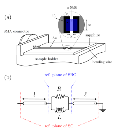
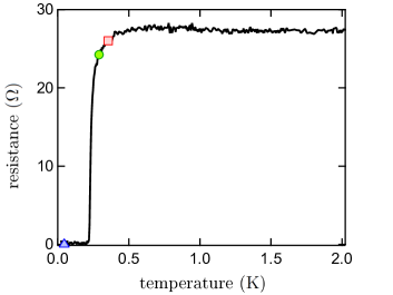
The sample here consists in an amorphous Nb15Si85 (a-NbSi) superconducting thin film of thickness =12.5 nm111The a-NbSi film has been prepared at room temperature and under ultrahigh vacuum (typically a few 10-8 mbar) by electron beam co-deposition of Nb and Si, at a rate of the order of 1 Å.s-1 as described in Couëdo et al. (2016).. In order to prevent any diffusion of gold into the a-NbSi film, a 25 nm-thick Pt buffer layer was inserted between the gold line and the sample as shown in the blow-up Fig. 3.a: on both sides of the samples the length of the Pt line is m. Indeed, platinum does not diffuse in a-NbSi and has the advantage of being a good conductor, non-magnetic – which is important when dealing with superconducting samples – and non-oxidizable to ensure a good ohmic contact with the thin film. The geometry of the a-NbSi film was tuned so that its normal state resistance () is close to : its width was m and its effective length m, which corresponds to the length of the NbSi film that becomes superconducting at low temperature. Indeed, we have checked in a separate experiment that, in regions where Pt and a-NbSi were superimposed, superconductivity was suppressed by inverse proximity effect, allowing for a clear definition of the calibration planes (see Fig.3(b)). Both the microstrip line and the sample were fabricated using standard photo-lithography and etching techniques.
Before any low temperature reflectometry measurements, we have characterized the room temperature frequency response of the sample by using a SC at port #3. As the incoming microwave arrives on the sample, the main impedance mismatch encountered is at the interface between the gold microstrip line and the sample. The reflection coefficient is then associated with a Fabry-Perot type resonator made out of the sample and of the second part of the gold microstrip line of length . It includes the -long line between the sample and the grounded plane and the length of the bonding wires connecting this plane to the ground. The phase associated with the propagation of the electromagnetic wave of frequency between the a-NbSi film and the ground is then given by with , the velocity of the electromagnetic wave in the microstrip. In the same way, a global phase is associated with the propagation along the SMA connector and the first part of the gold microstrip line, where stands for an effective propagation length that includes both the real microstrip line length and the effects of the SMA connector. then corresponds to the total impedance of the Fabry-Perot resonator, which is then related to the reflection coefficient according to:
| (3) |
where is the impedance of the a-NbSi film.
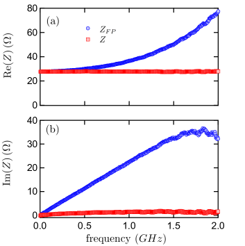
This electromagnetic model for the sample can be tested at room temperature. Fig. 4 shows the frequency dependance of both real and imaginary parts of . At low frequency, they are in good agreement with the sample impedance as measured by standard lock-in techniques: and . These values are consistent with what is expected for a metallic thin film, which geometry is such that we can neglect both the geometric inductance ( pH) and the capacitance to the ground ( fF). The sample is also sufficiently short to neglect any propagation effect for frequencies below a few hundreds MHz. At room temperature and low frequency, the a-NbSi thin film therefore behaves itself as a pure resistor. At higher frequencies, however, the effect of propagation in the Fabry-Perot resonator can be seen and the total impedance is no longer purely real. We can retrieve from , using equation (3). has been set by the geometry of the sample. was the only fitting parameter and has been adjusted so that and are frequency-independent on the whole frequency range. As can be seen, there is an excellent agreement between model and experiment for which is a realistic value for our setup. Moreover, it should be stressed that no additional capacitance was needed in the model to reproduce the data, in agreement with the result of a microwave simulation giving an upper limit of for the gap of in the microstrip line. This also rules out any parasitic effect coming from sample fabrication (remaining resist or contact resistances for eg.). At room temperature, the electromagnetic response of the ensemble microstrip + sample is therefore very well described by the sample resistance and Fabry-Perot type effects, as modeled by equation (3) and it enabled us to extract the value of the sample impedance at room temperature. In the following, and will be considered as fixed parameters.
In the rest of this paper, we will focus on the temperature and frequency dependences of the impedance in the low frequency limit , where is the superconducting energy gap. Below the critical temperature , the sample is superconducting and, within the two-fluid model approximation, behaves like a parallel circuit which parameters we will now evaluate. The a-NbSi sample is characterized by its electronic mean free path , its coherence length and its London penetration depth :
where is the diffusion constantAubin et al. (2006), is the Fermi velocity and the electron density. The Cooper pairs kinetic inductance at is then given by BCS theory in the dirty limit ():
| (4) |
where 26.5 is the normal state resistance of the sample. Since and since the dissipative part of the conductance is only due to unpaired electrons 222The dissipation given by the Mattis-Bardeen theory, related to thermally excited quasiparticles, will be discussed in Fig. 11(a)., the electromagnetic field penetrates all the sample and the parallel circuit in the low frequency limit is characterized by Tinkam (1975):
| (5) | |||||
| (6) |
where stands for the temperature dependence of the superconducting gap. In the following, although should, strictly speaking, be given by the self-consistent BCS gap equation, we will use the interpolation formula valid for close to . The overall complex impedance of the sample can thereby be written as:
| (7) |
We will now examine how the measured sample impedance compares with equation (7) for both the SC and the SBC. We should stress that the expression of given by equation (5) is nothing more than the Drude resistance and does not account for the dissipation related to thermally excited quasiparticles at finite frequencies. A more detailed study would use Mattis-Bardeen theory to describe the conductance of the superconducting film Mattis and Bardeen (1958), but we will see in section VI.4 that despite its simplicity, the two-fluid model captures the major part of the system’s physics.
V Standard calibration procedure
At first, let us consider the SC in which three references, an open, a short and a load (see Supplementary Material for more details on these standards), were successively connected to port #3 and cooled down at in order to determine the error coefficients, as described in Kitano et al. (2008); Reuss (2000). Once again, let us stress that our experimental set-up is not optimized for this measurement and that we have used this method solely to be able to compare it to our SBC on the same set-up. Figure 5 shows the frequency dependence of the reflexion coefficients for each of the standards at low temperature. As can be seen, the set-up response scarcely varies, within experimental uncertainty () in the 30 mK - 4 K. The sample was then measured during a fourth cool-down. In the SC procedure, the , and coefficients are directly given by:
where , and correspond to the measured reflection coefficient of the Open, Short and Load standards respectively. Using equations (1), (2) and (3), we retrieved the temperature and frequency dependences of the real and imaginary parts of the sample impedance, Re() and Im() (Fig. 6).
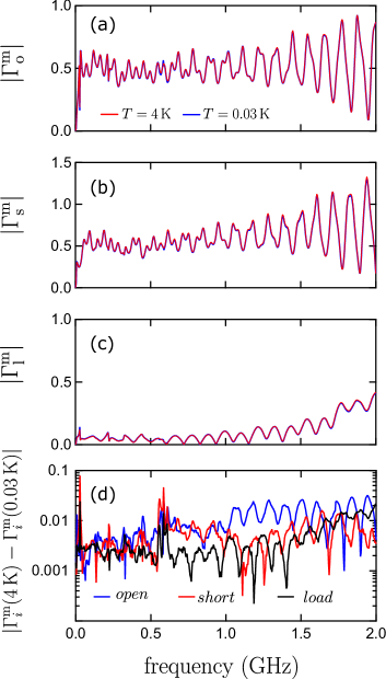
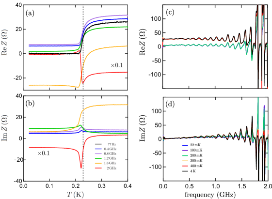
As can be seen, Re() follows qualitatively the expected temperature dependence at low frequency ()Mattis and Bardeen (1958); Driessen et al. (2012). In particular, is clearly identifiable through the drop in Re(). Concomitantly, Im() displays a maximum near , as expected from equation (7). However the low temperature values of both components exhibit a frequency-dependent offset that bears no physical ground. This is partly due to irreproducibility inherent to any cool-down. Thermal contractions, such as those in microwave cables or the contraction of the insulating dielectric in SMA-type connectors, may differ. Even in a cryogen-free dilution refrigerator, thermal gradients may be ill-controlled. These effects in turn give rise to cool-down-dependent impedance mismatches that are not taken into account by this calibration method. Moreover, the OSL standards may also have a different response at low temperature 333The evolution in the standards frequency response at low temperature was not corrected, although we have checked that the impedance of the load was still 50 at low temperature.. Finally, we have used parameters for the Fabry-Perot resonator (, ) that have been determined at room temperature and these may be slightly temperature-dependent. These effects are illustrated Fig. 7 where Fabry-Perot-type oscillations in the magnitude of and are flagrant at high frequency. As a result, the phase reference is ill-defined and the real and imaginary parts of are mixed up (Fig. 6(c), (d) and in Fig. 6(a), (b)).
Although our SC satisfactorily describes the qualitative features of the superconductor response at low frequency and might therefore be adequate to determine relative variations in , it is not appropriate to finely measure the absolute value of the sample impedance. As we will show in the following section, it is necessary to use a more precise calibration procedure to probe the frequency dependence of the dynamical response for a superconducting film.
VI Sample-based calibration procedure
VI.1 General principle
Remarking that the error coefficients (, and ) can be determined from any given set of three references, we propose a calibration procedure using the sample itself as reference. For this, we choose three temperatures, , and , each of them lower than , for which we know the sample impedance from a separate experiment or a model (see Fig. 8). Since the microwave response of the setup is temperature-independent at low temperature, this calibration is valid for all temperatures below 4 K. It is remarkable that this method also fully takes into account the sample environment, such as the lines impedance mismatch due to a varying resistance and dielectric constant at low temperature, the connectors tightening conditions, the coupler’s imperfections or even the Fabry-Perot resonances due to the sample geometry (see Fig. 3(b)). The choice of the reference temperatures is of importance for the measurement precision. In particular, as we will see, the corresponding sample impedances have to be sufficiently different.
In the present case, the first reference point was chosen so that the sample is in the normal region. Significant superconducting fluctuations could then be neglected (see Supplementary Material). We have also checked that the reactive part of the conductance due to weak localisation is negligible within the frequency range of the measurement (see Supplementary Material). For (), we therefore assumed the sample to be purely resistive, with an impedance given by the simultaneous lock-in measurement: .
The second reference point was also chosen for the sample to be in the normal state, albeit closer to . Given the normal state resistance value of the a-NbSi sample, we have established by varying the reference temperature that a minimum difference of is necessary to optimize the calibration signal–to–noise ratio. For , the result after calibration is unchanged, within experimental uncertainty, as will be discussed in section VI.3. We therefore chose . Should the normal state resistance be further away from 50 , a larger should be chosen. For this temperature, we have also assumed that , given by the lock-in measurement. As the superconducting transition is approached, Aslamazov-Larkin corrections of the DC conductivity have been shown to be relevant for our system Crauste (2010). However, from estimates of Aslamazov-Larkin conductivity corrections for Aslamasov and Larkin (1968); Ohashi et al. (2006), we have checked that the frequency dependence of could be neglected in the considered frequency range (see Supplementary Material).
The third reference point was taken such that = 25 mK . At these temperatures, usual superconductors can be assimilated to short circuits. This is the assumption made by Booth et al.Booth et al. (1994). However, in the case of disordered superconductors such as a-NbSi, the zero-temperature kinetic inductance is large (see eq. (4)), so that the sample is best modeled by a pure inductance . The zero-temperature kinetic inductance has been estimated using eq. (4) (see Supplementary Material). The error caused by the choice of will be discussed in section VI.4.
Although the sample complex impedance is, by definition of this method, fixed at , and , its temperature and frequency dependencies close to the superconducting transition are not imposed by the calibration, as shown in the following. We can therefore infer the sample electrodynamic response at all other temperatures, provided the knowledge of the sample impedance at the three calibration points.
VI.2 Definition of the calibration planes
As mentioned in section IV, the sample is inserted within a transmission line resulting in Fabry-Perot type interferences. One of the main strengths of the SBC procedure is that, although it may seem counter-intuitive, it redefines the calibration planes by taking into account the Fabry-Perot resonator (see Fig. 3(b)). Indeed, the references , and now correspond to measured reflection coefficients , and such that:
| (8) |
where the are defined by:
| (9) |
In other words, all the sample’s environment is taken into account in the three complex coefficients , and . Note that the detection setup will be most efficient when . By inserting these references into the calibration equations Kitano et al. (2008), one obtains the calibration coefficients:
| (10) | |||||
| (11) | |||||
| (12) |
where , , and . By inverting equations (1) and (2), we finally get the calibrated value of the impedance of the sample:
| (13) |
which can be expressed as a function of the measured values , , and the corresponding impedances , , :
| (14) |
where .
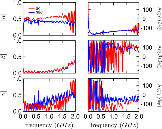
It is worth noting that the calibration coefficients deduced from the SC and the SBC procedures are different, as can be observed in Fig. 7. As can be expected, the magnitude of is almost the same for both calibration methods since it mainly reflects the properties of the coupler. However, both and strongly depend on the imperfections of the transmission line on port #3. In particular, both coefficients include the effect induced by the Fabry-Perot resonator and are therefore significantly different for . We also observe standing wave patterns on the frequency dependence of , and . These patterns are characterized by a frequency and correspond to multiple reflections in a -long cable which is consistent with the length of the detection line. These oscillations are again more pronounced in the case of the SC procedure because the calibration is performed in 4 successive coolings. In other words, the strength of the SBC procedure resides in the fact that the calibration planes flank the sample and are defined once for all measurements.
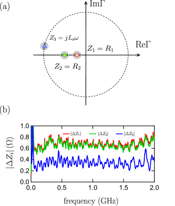
According to equations (10)-(12), the calibration coefficients are defined as soon as the references , and are different (Fig. 9(a)). However, the references have to be chosen so that the related reflection coefficients , and are clearly different from each others. From an experimental point of view, these coefficients are measured within a statistical uncertainty which depends on the noise of the cryogenic amplifier, its gain , the VNA output power and its resolution bandwidth :
| (15) |
The output power is chosen to avoid Joule heating and its upper limit can be related to the upper limit of the DC current . By comparing it to the microwave power absorbed by the sample, we find:
| (16) |
where stands for the attenuation on the excitation line and has been evaluated in the normal state ( 4 K). In the experiment, the excitation will be set to , i.e. on the sample. This gives rise to a statistical uncertainty . The determination of the calibration coefficients thus requires a minimal difference between the impedances of references , and :
| (17) |
Figure 9(b) shows as a function of frequency using the calibration coefficients deduced from the SBC. The various are essentially frequency-independent, except for the oscillating patterns, of caracteristic frequency 50 MHz, which are due to the standing waves along the 2 m-long cable of the detection line. From Eq. 17, the frequency dependence of is indeed not only due to the coefficient but also to . It is reasonable to assume that for all standards, . For security, we define a criterion for the choice of the references: they must be such that . The references described in section VI.1 were such that , which conforms to the criterion.
VI.3 Error on the calibration
As previously discussed, a minimal difference between standards is necessary to perform the calibration because of the random errors in the experimental measurements. However, a large difference in the references impedances does not mean the errors are small. The errors , and on calibration coefficients indeed induce systematic errors on impedance measurements. This errors read:
| (18) |
where is the random error on the reflection coefficients and is the systematic error on the reference impedances . To minimize , several measurements of the standards have been averaged as the temperature was slowing ramping (see Suplementary Material), so that it in turns introduces a small contribution to (for references and ). therefore includes the statistical uncertainty in the measurement of the standard response, the error introduced by a non-stabilized temperature and the error due to the assumptions made on .
, and are complex numbers, they are frequency–dependent and change for each calibration procedure. In the following, the calibration coefficients are averaged over 10 measurements (see Supplementary Material) to improve the quality of the calibration giving rise to:
| (19) | |||||
| (20) |
We will discuss the choice of in the next section (see also Suplementary Material). Our goal here is to determine the maximum error that one makes on the sample impedance using a given calibration procedure. By considering the random errors on the reflectometry measurements and the systematic errors on the calibration coefficients, we deduce from the root mean square error:
| (21) |
The first term corresponds to the statistical reproducibility of the measurement. The other terms are related to the systematic errors coming from the determination of the calibration coefficients. This quantity can be expressed as a function of the calibration coefficients and the measured impedance:
| (22) |
where and .
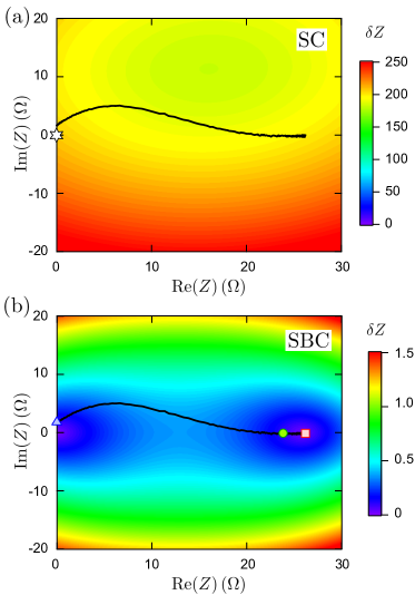
A numerical calculation using the calibration coefficients derived from both the SC and the SBC procedures enables to return the error as a color map in the impedance range of interest (Fig. 10). In the SC procedure, the three standards and the sample have been cooled down successively. The random error on the reflection coefficient is then no longer defined by the amplifier noise, but by the reproducibility of the cool-downs. Because we are working at dilution refrigerator temperatures, as mentioned in section II, numerous microwave components need to be inserted along the measurement setup (see Supplementary Material). The reflection of the line can then unavoidably differ by from one cooling to another (see Supplementary Material). When working at millikelvin temperature, it is thus preferable to develop a single-cooldown calibration. The random error on the reflection coefficient is thus . Then, the error on the impedance measurement (Fig. 10(a)) can reach as observed in Fig. 6. Figure 10(b) shows for the SBC procedure. It has been calculated by using the random errors on the refection coefficients and the systematic errors on the references as previously determined (see equations (19), (20) and (22)). Although the error on the SC could probably be minimized by optimizing the experimental set-up for this specific calibration, there is almost a difference of three orders of magnitude in the obtained between the two calibrations. For the SBC, the upper bound of the error will allow us to compare the calibrated data with theoretical expectations. The error in the SBC procedure is, as expected, minimal around the references impedances. This is not observed in the SC procedure because the calibration coefficients are deduced from three different coolings and do not exactly describe the microwave setup used to measure the sample. Note that if it had been possible to chose well separated reference impedances in the SBC procedure (as “open”, “short” and “load”) the precision of the measurement would have been better by one order of magnitude .
VI.4 Results
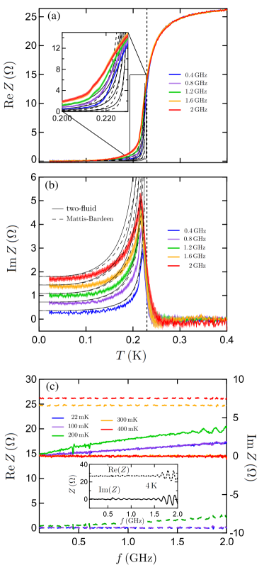
The sample impedance obtained after SBC is shown as a function of temperature and frequency in Fig. 11. Before analyzing the evolution of the sample impedance in temperature, let us point out the experimental robustness of the SBC method: Fig. 11.c shows the sample impedance as a function of frequency, at five selected temperatures. The inset of the same figure gives the sample impedance computed using the same calibration on data that were obtained at 4 K thirteen days before. As can be seen, the 4 K impedance is consistent with the DC measurement and the estimated errors except at frequencies higher than 1.5 GHz, probably due to the overall evolution of the measurement set-up. The shaded areas in Fig. 11.a and b correspond to the error . As expected, in the normal state, the impedance is purely real. At the superconducting transition, the maximum amplitude of Im() increases with frequency, due to the finite superfluid density developing at . Let us emphasize that the calibration imposes the sample response in the normal state at and in the superconducting state at . The divergence of the kinetic inductance responsible for the Im() peak thus cannot be explained by a calibration artefact.
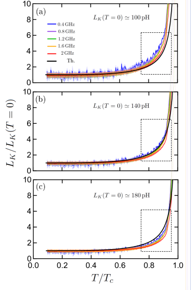
In Fig. 12, the kinetic inductance is plotted as a function of temperature, assuming that the reactive part of the electromagnetic response of the superconductor is well described by an inductance (see equation (6)): . This quantity clearly depends on the choice of the calibration reference . In order to assess the systematic error made when assigning a given value to , we have plotted in the different panels the result of the calibration for , and . These values correspond to a superconducting gap of , as has been measured on the same system by Scanning Tunneling Microscopy444C. Chapelier, C. Tonnoir, E. Driessen, unpublished.. When comparing the results of the calibration (color dots) with BCS theory (solid black line) on the whole temperature range, it is clear that the temperature dependence of is unaffected by the choice of , as is natural due to the influence of the reference . However, for , there is a deviation from the theory for and larger than the estimated maximum error (dashed rectangles in Fig. 12). The temperature evolution of hence allows us to justify a posteriori the choice of the calibration reference given by the BCS theory with an average gap value. In the following, we will fix for fixing the impedance value .
Let us now compare the results extracted from the SBC with the theoretical predictions for the temperature and frequency dependences of the sample impedance. The solid black lines in Fig. 11 corresponds to the theoretical expectation given by the two-fluid model where the BCS temperature dependence of the gap has been introduced (equations (5), (6) and (7)). While the qualitative features of the data can be reasonably well explained by this simple model, in particular at low frequency and far from , there is a discrepancy close to the sample critical temperature, both for and . The increase of with the frequency cannot be accounted for by a sole inductance. As shown in Fig. 11(a), the two-fluid model resistance deduced from the normal state (solid line) does not describe the experimental data and the dissipation related to thermally excited quasiparticles has to be taken into account. This dissipation corresponds to the coherence peak appearing close the in the real part of the Mattis-Bardeen conductance and could explain that we underestimate . However, the comparison with the Mattis-Bardeen theoryMattis and Bardeen (1958) (black dashed lines) – which should take the quasiparticles dissipation into account – does not yield a better agreement.
Thanks to the high precision on our measurements (see section VI.3), we can confidently say that the complex impedance of the superconducting a-NbSi thin film therefore departs from the theoretical expectations of BCS theory close to . There can be two main reasons for this. The first is an error in the assumptions we have made for , and . As has been detailed previously, we have checked that the assumptions that and were pure resistances whereas could be assimilated to a pure inductance were justified (see also Supplementary Material). Moreover, the electromagnetic model for the sample (Fig. 3(b)) has been tested and we have checked in a separate experiment that the Pt buffer layer in between the gold transmission line and the sample did not give rise to unaccounted dissipation effects. However, since these experiments are very sensitive, we cannot exclude spurious effects. The theory/experiment discrepancy could however also be the consequence of the disordered nature of these films. Indeed, thin a-NbSi films have been shown to exhibit disorder-induced Superconductor–to–Metal–to–Insulator Quantum Phase Transitions (QPT)Crauste et al. (2013); Couëdo et al. (2016). The theory of finite size scaling predicts a generalized scaling relation for the conductivity and thus an additional dependence in the conductance close to a QPTSondhi et al. (1997). This dependence has been observed experimentally in a-NbSi across the Metal–to–Insulator TransitionLee et al. (2000). Although the a-NbSi sample we study here is at a certain distance from the quantum critical point of the Superconductor–Insulator Transition, the QPT could indeed still manifest itself at . Moreover, such disordered films are known to exhibit Berezinskii–Kosterlitz–Thouless–type physics resulting in a depression of close to , for temperatures larger than the characteristic temperature , due to frequency-dependent phase fluctuationsMondal et al. (2011); Liu et al. (2011). These issues should be addressed in a systematic study of the electrodynamic response of a-NbSi superconducting thin films when disorder is varied. We would need to approach the critical points and cross to the metallic or insulating phases by studying samples with different niobium concentrations for instance. This will be the subject of a subsequent work.
VII Conclusion
In order to circumvent the issue of the low temperature calibration for microwave broadband measurements, we propose a calibration method which is based on the knowledge, whether experimental or theoretical, of the sample impedance at three different values of a tunable parameter. In the present work, we made use of the temperature dependence of the resistance, but the method could be extended to exploit a known magnetoresistance or the superconducting sample critical current for instance. Using these references, one can infer the absolute value of the sample complex impedance at all other temperatures, with an enhanced sensitivity due to the fact that this calibration fully takes into account the sample electromagnetic environment, provided the set-up is temperature-independent. Moreover, it only requires a single cool-down which makes the experiments easier to perform.
We would like to emphasize that any compound having a variation in impedance with any external parameter (not only the temperature but the electric field, the current, the magnetic field,….) could benefit from this calibration method. For instance, magnetic compounds, Josephson junction arrays Van der Zant et al. (1992) or mesoscopic circuits Gabelli et al. (2006) could be candidates. We could also think of 2D systems like graphene-based samples Han et al. (2014) and superconducting interfaces Singh et al. (2018), where a gate electric field can be used as a tuning parameter for the calibration. We therefore believe that this sample-based calibration method is very promising for characterizing the frequency dependence of condensed matter systems and could complement previously developed calibration methods.
Supplementary Material
See supplementary material for details on the microwaves lines of the set-up and the data acquisition protocole. Additional information are also given on the references that we used for the Standard Calibration (SC) as well as a discussion on the random error on the reflection coefficient for this SC. The assumptions made to define the references for the Sample-Based Calibration (SBC) are also precised.
Acknowledgements.
This work has been partially supported by the ANR (grant No. ANR 2010 BLAN 0403 01) and by the Triangle de la Physique (grant No. 2009-019T-TSI2D).References
- Scheffler and Dressel (2005) M. Scheffler and M. Dressel, Review of Scientific Instruments 76, 074702 (2005).
- Armitage (2009) N. Armitage, arXiv preprint arXiv:0908.1126 (2009).
- Dressel (2013) M. Dressel, Advances in Condensed Matter Physics 2013 (2013).
- Gabelli et al. (2006) J. Gabelli, G. Fève, J.-M. Berroir, B. Plaçais, A. Cavanna, B. Etienne, Y. Jin, and D. Glattli, Science 313, 499 (2006).
- Gabelli et al. (2007) J. Gabelli, G. Fève, T. Kontos, J.-M. Berroir, B. Plaçais, D. C. Glattli, B. Etienne, Y. Jin, and M. Büttiker, Physical Review Letters 98, 166806 (2007).
- Sachdev (1999) S. Sachdev, Quantum Phase Transitions (Cambridge University Press, 1999).
- Hafner et al. (2014) D. Hafner, M. Dressel, and M. Scheffler, Review of Scientific Instruments 85, 014702 (2014).
- Chen et al. (2004) L.-F. Chen, C. Ong, C. Neo, V. Varadan, and V. K. Varadan, Microwave electronics: measurement and materials characterization (John Wiley & Sons, 2004).
- Kubo et al. (2011) Y. Kubo, C. Grezes, A. Dewes, T. Umeda, J. Isoya, H. Sumiya, N. Morishita, H. Abe, S. Onoda, T. Ohshima, et al., Physical Review Letters 107, 220501 (2011).
- Dassonneville et al. (2013) B. Dassonneville, M. Ferrier, S. Guéron, and H. Bouchiat, Physical Review Letters 110, 217001 (2013).
- Reuss (2000) T. Reuss, Nouvel étalonnage cryogénique en réflectométrie (0.2 à 18 GHz) et application à l’étude de la dynamique des vortex de supraconducteurs HTc proche de Tc, Ph.D. thesis, Université Joseph-Fourier-Grenoble I (2000), https://tel.archives-ouvertes.fr/tel-00004277.
- Kitano et al. (2008) H. Kitano, T. Ohashi, and A. Maeda, Review of Scientific Instruments 79, 074701 (2008).
- Stutzman et al. (2000) M. Stutzman, M. Lee, and R. Bradley, Review of Scientific Instruments 71, 4596 (2000).
- Steinberg et al. (2012) K. Steinberg, M. Scheffler, and M. Dressel, Review of Scientific Instruments 83, 024704 (2012).
- Scheffler et al. (2015) M. Scheffler, M. M. Felger, M. Thiemann, D. Hafner, K. Schlegel, M. Dressel, K. S. Ilin, M. Siegel, S. Seiro, C. Geibel, et al., ACTA IMEKO 4, 47 (2015).
- Booth et al. (1994) J. Booth, D. H. Wu, and S. M. Anlage, Review of Scientific Instruments 65, 2082 (1994).
- Silva et al. (2016) E. Silva, N. Pompeo, K. Torokhtii, and S. Sarti, IEEE Transactions on Instrumentation and Measurement 65, 1120 (2016).
- Sarti et al. (2005) S. Sarti, C. Amabile, E. Silva, M. Giura, R. Fastampa, C. Ferdeghini, V. Ferrando, and C. Tarantini, Physical Review B 72, 024542 (2005).
- Meschede et al. (1992) H. Meschede, R. Reuter, J. Albers, J. Kraus, D. Peters, W. Brockerhoff, F.-J. Tegude, M. Bode, J. Schubert, and W. Zander, IEEE transactions on microwave theory and techniques 40, 2325 (1992).
- Orloff et al. (2011) N. D. Orloff, J. Mateu, A. Lewandowski, E. Rocas, J. King, D. Gu, X. Lu, C. Collado, I. Takeuchi, and J. C. Booth, IEEE Transactions on Microwave Theory and Techniques 59, 188 (2011).
- Cano and Artal (2009) J. L. Cano and E. Artal, Microwave Journal 52, 70 (2009).
- Yeh and Anlage (2013) J.-H. Yeh and S. M. Anlage, Review of Scientific Instruments 84, 034706 (2013).
- Ranzani et al. (2013) L. Ranzani, L. Spietz, Z. Popovic, and J. Aumentado, Review of Scientific Instruments 84, 034704 (2013).
- Limelette et al. (2003) P. Limelette, P. Wzietek, S. Florens, A. Georges, T. A. Costi, C. Pasquier, D. Jérome, C. Mézière, and P. Batail, Physical review letters 91, 016401 (2003).
- Gabelli and Reulet (2008) J. Gabelli and B. Reulet, Physical Review Letters 100, 026601 (2008).
- Note (1) The a-NbSi film has been prepared at room temperature and under ultrahigh vacuum (typically a few 10-8 mbar) by electron beam co-deposition of Nb and Si, at a rate of the order of 1 Å.s-1 as described in Couëdo et al. (2016).
- Aubin et al. (2006) H. Aubin, C. A. Marrache-Kikuchi, A. Pourret, K. Behnia, L. Bergé, L. Dumoulin, and J. Lesueur, Phys. Rev. B 73, 094521 (2006).
- Note (2) The dissipation given by the Mattis-Bardeen theory, related to thermally excited quasiparticles, will be discussed in Fig. 11(a).
- Tinkam (1975) M. Tinkam, Introduction to superconductivity (Krieger, 1975).
- Mattis and Bardeen (1958) D. Mattis and J. Bardeen, Physical Review 111, 412 (1958).
- Driessen et al. (2012) E. Driessen, P. Coumou, R. Tromp, P. De Visser, and T. Klapwijk, Physical Review Letters 109, 107003 (2012).
- Note (3) The evolution in the standards frequency response at low temperature was not corrected, although we have checked that the impedance of the load was still 50 at low temperature.
- Crauste (2010) O. Crauste, Study of Quantum Phase Transition Superconductor – Insulator, Metal – Insulator in disordered, amorphous materials near the dimension 2, Ph.D. thesis, Université Paris Sud - Paris XI (2010), https://tel.archives-ouvertes.fr/tel-00579256v1.
- Aslamasov and Larkin (1968) L. Aslamasov and A. Larkin, Physics Letters A 26, 238 (1968).
- Ohashi et al. (2006) T. Ohashi, H. Kitano, A. Maeda, H. Akaike, and A. Fujimaki, Physical Review B 73, 174522 (2006).
- Note (4) C. Chapelier, C. Tonnoir, E. Driessen, unpublished.
- Crauste et al. (2013) O. Crauste, A. Gentils, F. Couedo, Y. Dolgorouky, L. Bergé, S. Collin, C. Marrache-Kikuchi, and L. Dumoulin, Phys. Rev. B 87, 144514 (2013).
- Couëdo et al. (2016) F. Couëdo, O. Crauste, A.-A. Drillien, V. Humbert, L. Bergé, C. Marrache-Kikuchi, and L. Dumoulin, Scientific Reports 6 (2016).
- Sondhi et al. (1997) S. Sondhi, S. Girvin, J. Carini, and D. Shahar, Rev. Mod. Phys. 69, 315 (1997).
- Lee et al. (2000) H. L. Lee, J. P. Carini, D. V. Baxter, W. Henderson, and G. Gruner, Science 287, 633 (2000).
- Mondal et al. (2011) M. Mondal, A. Kamlapure, M. Chand, G. Saraswat, S. Kumar, J. Jesudasan, L. Benfatto, V. Tripathi, and P. Raychaudhuri, Physical review letters 106, 047001 (2011).
- Liu et al. (2011) W. Liu, M. Kim, G. Sambandamurthy, and N. Armitage, Physical Review B 84, 024511 (2011).
- Van der Zant et al. (1992) H. Van der Zant, F. Fritschy, W. Elion, L. Geerligs, and J. Mooij, Physical review letters 69, 2971 (1992).
- Han et al. (2014) Z. Han, A. Allain, H. Arjmandi-Tash, K. Tikhonov, M. Feigel’man, B. Sacépé, and V. Bouchiat, Nature Physics 10, 380 (2014).
- Singh et al. (2018) G. Singh, A. Jouan, L. Benfatto, F. Couëdo, P. Kumar, A. Dogra, R. Budhani, S. Caprara, M. Grilli, E. Lesne, et al., Nature communications 9, 407 (2018).