Simultaneous conduction and valence band quantisation in ultra-shallow, high density doping profiles in semiconductors
Abstract
We demonstrate simultaneous quantisation of conduction band (CB) and valence band (VB) states in silicon using ultra-shallow, high density, phosphorus doping profiles (so-called Si:P -layers). We show that, in addition to the well known quantisation of CB states within the dopant plane, the confinement of VB-derived states between the sub-surface P dopant layer and the Si surface gives rise to a simultaneous quantisation of VB states in this narrow region. We also show that the VB quantisation can be explained using a simple particle-in-a-box model, and that the number and energy separation of the quantised VB states depend on the depth of the P dopant layer beneath the Si surface. Since the quantised CB states do not show a strong dependence on the dopant depth (but rather on the dopant density), it is straightforward to exhibit control over the properties of the quantised CB and VB states independently of each other by choosing the dopant density and depth accordingly, thus offering new possibilities for engineering quantum matter.
There has been a surge of interest in two-dimensional (2D) materials due to their remarkable quantum properties. Graphene and layered transition metal dichalcogenides are just two examples of such materials that have been recently studied and proffered as advantageous for developing quantum electronic devices Novoselov et al. (2004, 2007); Mak et al. (2014); Xu et al. (2014). A rather unique branch of the 2D material family are ultra-shallow, high-density, doping profiles in semiconductors, so-called -layers. In particular, phosphorus -layers in silicon (Si:P -layers) combined with atomically precise lithography have led to recent technological successes towards scalable qubit architectures Fuechsle et al. (2012); Weber et al. (2012); Hill et al. (2015); McKibbin et al. (2013). It has been demonstrated that P donors, which can act as qubits, in Si have long spin lifetimes Suzuki et al. (2011); Wolfowicz et al. (2013) which are essential for spin-based quantum calculations. Importantly, Si:P -layers can be readily synthesized – they are comprised of a Si(001) substrate with a high density P dopant profile situated a few nanometers beneath an epitaxial grown Si encapsulation layer – and they are potentially straightforward to integrate into existing Si-based technology. Both the dopant layer and the encapsulation layer can be easily modified during the growth process Goh et al. (2004, 2006); Goh and Simmons (2009), and it is this flexibility that makes -layers so promising, not only for enhancing the performance of quantum electronic devices, but for engineering new 2D materials with new capabilities.
The confinement of a high density, atomically thin layer of P atoms beneath the surface abruptly changes the potential within the Si crystal. This brings about strong bending of the conduction band (CB) and valence band (VB) around the dopant plane, leading to strong confinement of the silicon CB. This strong confinement results in lowering and discretisation of the CB and consequently gives the system metallic character Carter et al. (2009, 2011); Miwa et al. (2013); Polley et al. (2012, 2013). These CB states have been studied in considerable detail Miwa et al. (2013, 2014); Mazzola et al. (2014a, b), and it has been determined that their binding energy and energy separation (so-called valley splitting) can be effectively controlled and tuned by varying the P doping density and/or depth profile Mazzola et al. .
It is not only essential for device operation and performance that the quantised CB states can be tuned and controlled but also their VB counterparts. We demonstrate a general method based on -doping to realise simultaneous quantisation of CB and VB electrons by structuring the band bending at the nanoscale. We show, using angle-resolved photoemission spectroscopy (ARPES), that quantised VB states arise from confinement between the P dopant layer and surface of the Si encapsulation. We verify that these quantised VB states can be tuned by varying the thickness of the Si encapsulation. This capability promises new prospects in engineering quantum matter, for example, the possibility of controlling carrier lifetimes by modifying the interaction between quantised CB and VB states.
ARPES measurements were performed at the I4 beamline at the MAX-III synchrotron radiation source Jensen et al. (1997). The energy and momentum resolutions were better than meV and Å-1, respectively. The base pressure in the analysis chamber was mbar, and the temperature of the sample was maintained at room temperature throughout data acquisition. The Si:P -layer samples were prepared by growing epitaxial Si (thicknesses from to nm) on top of 0.25 monolayers of P atoms incorporated in the topmost layer of a clean Si(001) substrate; a detailed recipe can be found in Ref. Miwa et al., 2013. The arrangement of incorporated P atoms in the Si substrate has been investigated by combined atom-resolved scanning tunnelling microscopy Curson et al. (2004) and density functional theory Wilson et al. (2006). The results of these studies suggest the incorporated P atoms exhibit some short- but no long-range ordering. Control samples were measured for comparison, and fabricated by growing a similar amount of epitaxial Si directly on the clean Si(001) substrate without the inclusion of a P-rich layer.
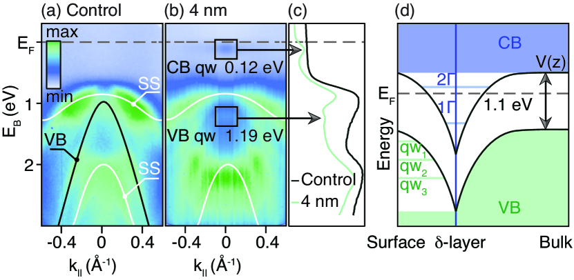
The ARPES acquisitions of a control sample and a Si:P -layer sample with an approximate 4 nm thick Si encapsulation layer are presented in Fig. 1(a) and (b), respectively. The two samples have similar spectral features: the VB dispersion around the point of the 2D Brillouin zone and surface states (SS) are consistent with bulk and surface states previously reported for electronic structure measurements of Si(001) with a 21 reconstructed surface Johansson et al. (1990a, b).
The Fermi level () lies within the 1.1 eV band gap and situated in close proximity to the conduction band minimum (CBM); confirming the n-type doping. There are notable differences between the two samples: an additional feature near and extra bands in the VB region — marked by the black rectangles — can be seen in the ARPES data of the Si:P -layer sample shown in Fig. 1(b). These differences are prominent in Fig. 1(c) where energy distribution curves (EDCs), integrated over a momentum range of -0.15 to 0.15 Å-1, are plotted. The additional states appear as peaks at binding energies of 0.12 eV and 1.19 eV for the Si:P -layer sample (green curve) and are noticeably absent in the control sample (black curve).
We use the band bending diagram of a Si:P -layer in Fig. 1(d) to illustrate the origin of these additional states. As we go from bulk to surface, i.e. from right to left across the diagram, the bulk CB becomes partially occupied in the region around the high density P dopant plane thereby creating a confined metallic layer. The CB states which are bound by the Coulomb-like potential well are labelled 1 and 2. Whilst these electronic states have already been studied in detail by ARPES Miwa et al. (2014), an understanding of the nature and origin of the extra bands that are visible in the VB region is lacking. Previous ARPES measurements have shown that both the CB and VB states are non-dispersing with photon energy, firmly establishing the 2D character of these co-existing states Miwa et al. (2013). ARPES acquisitions at photon energy of 36 eV are only presented here, as the intensity of the CB states is known to be enhanced at this energy Miwa et al. (2013); Mazzola et al. (2014b).
If VB states should exist between the surface and the -layer, they too must be strongly confined since both the surface and the -layer act as a barrier (see left side of Fig. 1(d)). Therefore, the hole-like bands of the VB become trapped like a particle-in-a-box, where the confinement width is dictated by the depth of the -layer beneath the surface and the confinement potential is dictated by the Fermi level pinning at the surface and at the -layer. All of these parameters can be controlled during the sample growth.
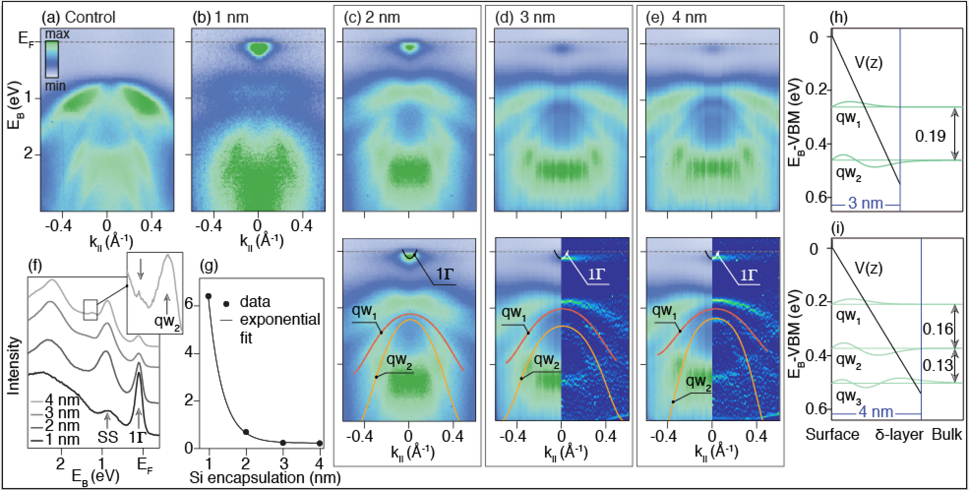
We have explored the influence of Si encapsulation layer thickness on the quantisation of CB and VB states using ARPES. First of all, we want to study the thickness dependent photoemission intensity, as this will give information about whether a certain electronic state is bulk or surface derived. In Fig. 2(b-e) we consider the following Si encapsulation thicknesses: 1 nm, 2 nm, 3 nm, 4 nm and compare them with the ARPES measurements for the control sample shown in Fig. 2(a). At first glance, all of the ARPES spectra of the different Si:P -layer samples appear qualitatively similar to each other. A pronounced difference is the diminishing spectral weight of 1 near the for Si:P -layers with thicker encapsulation. Since 1 originates from the P dopant layer situated beneath the surface, it is expected that the signal intensity gets weaker for thicker Si encapsulations. In Fig. 2(f), EDCs (integrated over a momentum range of -0.15 to 0.15 Å-1) are plotted for the control sample and the four Si:P -layers. In this manner, the peak intensities of both the CB and VB quantised states, marked by the arrows, can be directly compared. For increasing Si encapsulation thicknesses, a decrease in the intensity of the quantised CB peak corresponds to an increase in the intensity of the quantised VB states. This is confirmed in Fig. 2(g) where the spectral intensity of the CB is plotted (relative to the intensity of the VB states, i.e. /), as a function of Si encapsulation thickness and shows an exponential suppression for photoelectrons emitted from deeper P dopant layers. Whilst the sub-surface origin of the quantised CB states was known, this analysis suggests that the quantised VB states exist up to the surface.
By increasing the thickness of the encapsulation from 3 nm to 4 nm, the energy separation between the quantised VB states decreases; compare qw1 (orange) and qw2 (yellow) in Fig. 2(d and e). This trend can be explained by a particle-in-a-box picture: as the width of the box, or in this case the thickness of the Si encapsulation, is increased, the energies of the quantum states are lowered. We note that the energy separation between the quantised VB states for the 2 nm encapsulation thickness (Fig. 2(c)) does not follow this trend. This exception may be due to the complex interaction of the SS, located at 1 eV, with the quantised VB states. While the physical extent of the SS wave function is relatively shallow Yengui et al. (2015), a broadening and shifting could still be expected for a sufficiently small spatial separation of the SS and the quantised VB states.
The dispersion of the quantised VB states was fitted using an even sixth-order polynomial (orange and yellow curves in Fig. 2), and their effective masses and uncertainties estimated SM (2). We expect the different encapsulation thicknesses to have a small affect on the effective masses of the quantised VB states. Given the associated uncertainties, the effective masses for the qw1 state are in agreement with the heavy-hole state in the bulk VB of Si. The effective masses for the qw2 state are less, but also probably derived from the bulk heavy-holes since their effective masses are more similar to that of the bulk heavy-hole state than the bulk light-hole state.
Additional confirmation that the extra features in the VB region are quantised VB states confined within the Si encapsulation layer is provided by our numerical model for solving the Schrödinger equation presented in Fig. 2(h and i). For simplicity we only consider a linear potential (, black line) between the dopant layer and the surface. The approximation is crude but reproduces the quantised VB states seen in the ARPES measurements of Fig. 2. It is worth noting that we only apply our model to Si:P -layers with the thickest encapsulation layers studied here, i.e. nm and nm, since the quantised VB states and the surface states are well separated for these cases thereby facilitating the comparison between data and model. The interaction of the SS with the quantised VB states, for the nm and nm cases, is simply not captured in this model that assumes a quantum well with the same boundary conditions for every thickness.
In our model by increasing the thickness from 3 to 4 nm, the number of solutions to the Schrödinger equation increases from two to three. For the 3 nm case, the two calculated states are assigned to the qw1 and qw2 states observed in the experiment; see Fig. 2(d). The experimental data in Fig. 2(e) shows a weak hint of a third qw3 state expected for the 4 nm case but the intensity of the signal is weak and comparable to the background. The reduced intensity of the state may also be a result of its wave function being less localised at the surface (compared to qw1 & qw2) as illustrated in Fig. 2(i), or due to the fact that the photoionisation cross-section of this state is lower at this photon energy Miwa et al. (2013) (or, most likely, both effects might play a role).
We extracted EDCs, integrated over a finite momentum range, for Si:P -layers with different encapsulation thicknesses to investigate further this possible qw3 state. In the inset of Fig. 2(f), the qw2 state is readily visible for the 4 nm thick Si encapsulation data, and adjacent to this state, there is a small peak where the qw3 state may be expected.
The energy separations between the quantised VB states are determined from the numerical model to be: qw2-qw1=0.19 eV for the nm thick Si encapsulation, and qw2-qw1=0.16 eV and qw3-qw2=0.13 eV for the nm thick layer. From the experimental data we measure an energy separation between the two lowest lying states to be qw2-qw1= eV for the 3 nm thick Si encapsulation and qw2-qw1= eV for the 4 nm thick layer, respectively (3 nm: qw eV and qw eV, nm: qw eV and qw eV). The experimental values for all the quantised VB states are different from the ones extracted numerically, however the general trend holds for the thicker encapsulation thicknesses: (i) a shift of the quantised states toward lower binding energy and (ii) a decrease in the energy separation between higher to lower lying states for increasing Si encapsulation thickness is observed. This supports the notion that the quantised VB states originate from confinement in the Si encapsulation layer. We expect that a more accurate model for the doping potential and its recovery to the surface, including the influence of the SS wave function, might be able to give more realistic energy separations.
Simultaneous quantisation of CB and VB has not been demonstrated in common semiconductors, previously, a special case of simultaneous quantisation of the CB and VB has been reported for the topological insulator Bi2Se3 Bianchi et al. (2011). The adsorption of CO gas on the Bi2Se3 surface induces a similar downward band bending of the CB and the formation of quantised CB states. However, the quanitsed VB has quite another origin: Bi2Se3 has a peculiar valence electronic structure near the centre of its surface Brillouin zone — in this region the upper VB only exists in a narrow (200 meV) energy window — and thus downward bending of the VB can also lead to quantised states. The origin of the CB and VB quantisation is completely different in a -layer since the simultaneous quantisation of the CB and VB is purely artificial: it is dictated by the type, density and profile of the dopant layer and unlike Bi2Se3 is not an innate and unusual property of the bulk material. Artificially induced quantisation of the CB and VB by -doping offers the realisation of the same effect in a wide spectrum of semiconductor hosts.
The properties of the band-bending in -layers can be easily modified during the growth process, and as a result quantisation of the CB and VB can be controlled and tuned. We can, for example, also occupy the 2 state so that it is situated below the Miwa et al. (2014); Mazzola et al. , by either increasing the P dopant density or broadening the P dopant profile of the -layer. The surface of the Si encapsulation layer will similarly impact the quantisation of the VB states as different surface terminations or surface adsorbates can alter the pinning at the surface, and thus modify the degree of band bending between the dopant layer and the surface.
The situation of simultaneous quantisation of electron and hole states is a rather unusual effect Bianchi et al. (2011), never observed before in traditional doped semiconductors. This effect provides the appealing prospect of controlling the lifetime of carriers, creating additional channels to generate electron-hole pair recombinations in the CB, mediated by electronic transitions from the VB, potentially controlled by a biased top gate (analogous to a field effect transistor). That is, to mediate transitions between the CB and VB by tuning the potential landscape in which these states reside by modification of the dopant layer and the surface termination. For example, surface doping would directly influence the barrier potential responsible for the near-surface quantised VB states, and thus directly influence their energy, but would have a minimal influence on the sub-surface quantised CB (and bulk VB), for which the -layer and bulk doping densities, respectively, determine the Fermi level pinning. Thus, by modifying the surface potential, it should be possible to deliberately align (or misalign) the energies of the quanitised VB and CB states so as to exhibit control of their interaction (and therefore lifetime). The flexibility that these -layers offer could be expected to play a major role in the performance of quantum electronic devices.
In summary, simultaneous quantisation of the CB and VB states of Si:P -layers has been experimentally verified using ARPES. The origins of these quantised states are different: the CB states arise from the potential well induced by the ultra-dense dopant layer whereas the VB states originate from confinement between the potential well created by the dopant layer, and the sample surface. All of the relevant properties of both the dopant and encapsulation layers can be easily controlled and modified during the -layer growth process; not only providing the ability to exhibit control the quantisation of CB and VB states, but also offering the intriguing possibility of influencing lifetimes within the -layer structure, thereby opening up new possibilities for engineering quantum materials with new capabilities.
Acknowledgements: We acknowledge Johan Adell for support at the I4 beamline at MAX-III. Partial funding for this work was obtained through the Norwegian PhD Network on Nanotechnology for Microsystems sponsored by the Research Council of Norway, Division for Science under contract no. 221860/F40. J.A.M. acknowledges support from the Danish Council for Independent Research, Natural Sciences under the Sapere Aude program (Grant no. DFF-6108-00409) and the Aarhus University Research Foundation. This work was supported by VILLUM FONDEN via the Centre of Excellence for Dirac Materials (Grant No. 11744) and partly supported by the Research Council of Norway through its Centres of Excellence funding scheme, project number 262633, “QuSpin”, and through the Fripro program, project number 250985 “FunTopoMat”.
References
- Novoselov et al. (2004) K. S. Novoselov, A. K. Geim, S. V. Morozov, D. Jiang, Y. Zhang, S. V. Dubonos, I. V. Grigorieva, and A. A. Firsov, Science 306, 666 (2004).
- Novoselov et al. (2007) K. S. Novoselov, Z. Jiang, Y. Zhang, S. V. Morozov, H. L. Stormer, U. Zeitler, J. C. Maan, G. S. Boebinger, P. Kim, and A. K. Geim, Science 315, 1379 (2007).
- Mak et al. (2014) K. F. Mak, K. L. McGill, J. Park, and P. L. McEuen, Science 344, 1489 (2014).
- Xu et al. (2014) X. Xu, W. Yao, D. Xiao, and T. F. Heinz, Nat. Phys. 10, 343 (2014).
- Fuechsle et al. (2012) M. Fuechsle, J. A. Miwa, S. Mahapatra, H. Ryu, S. Lee, O. Warschkow, L. C. L. Hollenberg, G. Klimeck, and M. Y. Simmons, Nat. Nanotechnol. 7, 242 (2012).
- Weber et al. (2012) B. Weber, S. Mahapatra, H. Ryu, S. Lee, A. Fuhrer, T. C. G. Reusch, D. L. Thompson, W. C. T. Lee, G. Klimeck, L. C. L. Hollenberg, et al., Science 335, 64 (2012).
- Hill et al. (2015) C. D. Hill, E. Peretz, S. J. Hile, M. G. House, M. Fuechsle, S. Rogge, M. Y. Simmons, and L. C. L. Hollenberg, Sci. Adv. 1, e1500707 (2015).
- McKibbin et al. (2013) S. R. McKibbin, G. Scappucci, W. Pok, and M. Y. Simmons, Nanotechnology 24, 045303 (2013).
- Suzuki et al. (2011) T. Suzuki, T. Sasaki, T. Oikawa, M. Shiraishi, Y. Suzuki, and K. Noguchi, Appl. Phys. Expr. 4, 023003 (2011).
- Wolfowicz et al. (2013) G. Wolfowicz, A. M. Tyryshkin, R. E. George, H. Riemann, N. V. Abrosimov, P. Becker, H.-J. Pohl, M. L. W. Thewalt, S. A. Lyon, and J. J. L. Morton, Nat. Nanotechnol. 8, 561 (2013).
- Goh et al. (2004) K. E. J. Goh, L. Oberbeck, M. Y. Simmons, A. R. Hamilton, and R. G. Clark, Appl. Phys. Lett. 85, 4953 (2004).
- Goh et al. (2006) K. E. J. Goh, L. Oberbeck, M. Y. Simmons, A. R. Hamilton, and M. J. Butcher, Phys. Rev. B 73, 035401 (2006).
- Goh and Simmons (2009) K. E. J. Goh and M. Y. Simmons, Appl. Phys. Lett. 95, 142104 (2009).
- Carter et al. (2009) D. J. Carter, O. Warschkow, N. A. Marks, and D. R. McKenzie, Phys. Rev. B 79, 033204 (2009).
- Carter et al. (2011) D. J. Carter, N. A. Marks, O. Warschkow, and D. R. McKenzie, Nanotechnology 22, 065701 (2011).
- Miwa et al. (2013) J. A. Miwa, P. Hofmann, M. Y. Simmons, and J. W. Wells, Phys. Rev. Lett. 110, 136801 (2013).
- Polley et al. (2012) C. M. Polley, W. R. Clarke, J. A. Miwa, M. Y. Simmons, and J. W. Wells, Appl. Phys. Lett. 101, 262105 (2012).
- Polley et al. (2013) C. M. Polley, W. R. Clarke, J. A. Miwa, G. Scappucci, J. W. Wells, D. L. Jaeger, M. R. Bischof, R. F. Reidy, B. P. Gorman, and M. Simmons, ACS Nano 7, 5499 (2013).
- Miwa et al. (2014) J. A. Miwa, O. Warschkow, D. J. Carter, N. A. Marks, F. Mazzola, M. Y. Simmons, and J. W. Wells, Nano Lett. 14, 1515 (2014).
- Mazzola et al. (2014a) F. Mazzola, C. M. Polley, J. A. Miwa, M. Y. Simmons, and J. W. Wells, Appl. Phys. Lett. 104, 173108 (2014a).
- Mazzola et al. (2014b) F. Mazzola, M. T. Edmonds, K. Høydalsvik, D. J. Carter, N. A. Marks, B. C. C. Cowie, L. Thomsen, J. Miwa, M. Y. Simmons, and J. W. Wells, ACS Nano 8, 10223 (2014b).
- (22) F. Mazzola, J. A. Miwa, R. Rahman, X.-G. Zhu, M. Simmons, P. Hofmann, and J. Wells, in progress.
- Jensen et al. (1997) B. Jensen, S. Butorin, T. Kaurila, R. Nyholm, and L. Johansson, Nucl. Instrum. Methods in Phys. Res. A 394, 243 (1997).
- Curson et al. (2004) N. J. Curson, S. R. Schofield, M. Y. Simmons, L. Oberbeck, J. L. O’Brien, and R. G. Clark, Phys. Rev. B 69, 195303 (2004).
- Wilson et al. (2006) H. F. Wilson, O. Warschkow, N. A. Marks, N. J. Curson, S. R. Schofield, T. C. G. Reusch, M. W. Radny, P. V. Smith, D. R. McKenzie, and M. Y. Simmons, Phys. Rev. B 74, 195310 (2006).
- Johansson et al. (1990a) L. S. O. Johansson, P. E. S. Persson, U. O. Karlsson, and R. I. G. Uhrberg, Phys. Rev. B 42, 8991 (1990a).
- Johansson et al. (1990b) L. S. O. Johansson, R. I. G. Uhrberg, P. Mårtensson, and G. V. Hansson, Phys. Rev. B 42, 1305 (1990b).
- Zhang et al. (2011) P. Zhang, P. Richard, T. Qian, Y.-M. Xu, X. Dai, and H. Ding, Rev. of Sci. Instrum. 82, 043712 (2011).
- SM (1) See Supplementary Material for details regarding the fit analysis.
- Yengui et al. (2015) M. Yengui, H. P. Pinto, J. Leszczynski, and D. Riedel, J. of Phys.: Condens. Matter 27, 045001 (2015).
- SM (2) See Supplementary Material for details regarding the estimates of the effective masses.
- Bianchi et al. (2011) M. Bianchi, R. C. Hatch, J. Mi, B. B. Iversen, and P. Hofmann, Phys. Rev. Lett. 107, 086802 (2011).