VO2 as a natural optical metamaterial
Abstract
VO2 is a unique phase change material with strongly anisotropic electronic properties. Recently, samples have been prepared that present a co-existence of phases and thus form metal-insulator junctions of the same chemical compound. Using first principles calculations, the optical properties of metallic and semiconducting VO2 are here discussed to design self-contained natural optical metamaterials, avoiding coupling with other dielectric media. The analysis of the optical properties complements the experiments in the description of the vast change in reflectance and metallicity for both disordered and planar compounds. The present results also predict the possibility to realize ordered VO2 junctions operating as efficient hyperbolic metamaterials in the THz-visible range, by simply adjusting the ratio between metallic and insulating VO2 content. The possibility to excite propagating volume plasmom polariton across the metamaterial is finally discussed.
I Introduction
Optical metamaterials (OMMs) Cai:1339104 are artificially nanostructured compounds that exhibit an unconventional optical response to light that is unavailable in natural materials. Although the field of metamaterials started with the search of the so-called double negative materials (or Veselago media) 0034-4885-68-2-R06 , the idea of realizing artificial materials that can be engineered to support unique electromagnetic modes in the subwavelength regime opened up new conceptual frontiers for OMMs, which rapidly surpassed the concept of negative refraction. This has fostered the research of a new class of tunable and active metamaterials, known as hyperbolic metamaterials (HMMs) Poddubny:2013cy .
HMMS are highly anisotropic uniaxial materials that derive their name from the topology of the isofrequency surface (k)=constant. In uniaxial materials, the dielectric and the permeability tensors can be written in a diagonal form, in terms of the four fundamental parameters (), where the subscripts and indicate components parallel and perpendicular to the anisotropy () axis. If one out of the four fundamental parameters is negative, the isofrequency surface opens into a hyperboloid. For non-magnetic materials, the choice , corresponds to a two-fold hyperboloid and the medium is called a type-I metamaterial; the choice , describes a one-fold hyperboloid and the medium is called a type-II material. These unusual characteristics open the way to a wide range of unprecedented applications such as negative refraction Hoffman:2007jt , sub-diffraction imaging Jacob:06 , subwavelength waveguides Ishii:2013er , and spontaneous emission engineering 2040-8986-14-6-063001 .
Hyperbolic electric dispersion is typically realized by using artificial nanostructures, such as multilayers of alternating sub-wavelength layers of metals and dielectrics or assemblies of metallic nanowires embedded in a dielectric host. The choice of the structural parameters (e.g., thickness and number of layers) as well as of the constituting materials affects the optical and plasmonic properties of the HMM as well as the frequency range of their working application. On one hand, manufacturing of artificial HMMs is still a challenge as it requires ordered growth in the sub-wavelength scale of different materials with potentially different crystalline characteristics and/or growth conditions. On the other hand, the discovery of natural HMMs Narimanov2015 ; Sun:2014kg – i.e. uniaxial single-phase materials with opposite sign of permittivity – would offer a viable alternative to artificial metal-dielectric composites. However, the hyperbolic requirement is a rare condition and only few systems (such as graphite-like materials, cuprate and ruthenate perovskites) have been identified as natural HMMs up to now Korzeb:2015fv .
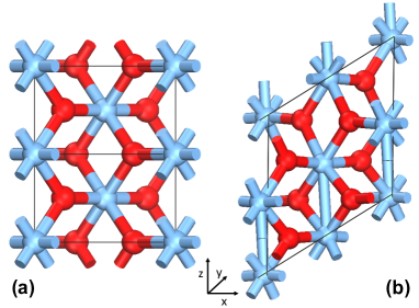
In this regard, phase change materials (PCMs) may constitute a valuable compromise for the realization of HMMs, playng with different phases, rather than different materials, thus reducing defect and strain content. Vanadium dioxide (VO2) in particular has shown promise due to its metal-to-insulator transition (MIT) RevModPhys.70.1039 at the critical temperature of 340K Kucharczyk1979 . The MIT in VO2 occurs when the atoms in the metallic structure dimerize and break the crystal symmetry, resulting in a shift from a tetragonal rutile (R) phase to a low temperature monoclinic (M1) phase (Fig. 1). The optical properties differ widely between phases, making it possible to realize switchable devices based on altering the absorption, conductivity, or reflectance of the material by precise control of the system environment. In fact, schemes are already in place to implement VO2 in switching plasmonic nanoantenna, Abate2015 ultrafast light emission modulators Cueff2015 , near-field thermal transfer devices Menges2016 , and novel optical metamaterials Rensberg2016 ; Krishnamoorthy2014 , in connection with other dielectric oxides (e.g. sapphire Rensberg2016 , titania acsnano.6b05736 , silicaWen:2010gg ) or conducting media (e.g. Au Liu:2012fw , Al:ZnOPhysRevApplied.8.014009 ).
Additionally, recent experiments have shown that it is possible to create VO2 samples containing a co-existent mixture of both phases, i.e. to create a compound that combines the original metallic and dielectric behavior of the separate phases into a brand new metamaterial, with intrinsic optical properties different from the ones of the original constituents. This characteristic renders VO2 a unique PCM. These VO2 mixtures have often been induced through chemical doping Strelcov2016 , temperature gradients Abate2015 ; Savo2015 , strain Wang2016 , charge injection doi:10.1021/nl9028973 , or ion beam irradiation Rensberg2016 . While several experiments have been able to accurately model the optical constants of inhomogeneous Kats2012 ; Qazilbash2007 or two-dimensional Rensberg2016 VO2 metamaterial at a target wavelength, a comprehensive study of the effective optical properties of mixed-phase VO2 across a broad range of energy and composition is still lacking.
On the theoretical side, the majority of first principles investigations remained focused on describing the electronic band structure and characterizing the mechanism behind MIT Brito2016 ; Weber2012 ; Eyert2011 , while modelling of their plasmonic properties uses empiric parameters extrapolated from experiments Wen:2010gg ; Yahiaoui:2017jy . In particular, the use of empirical data suffers from lack of transferability, as they are strictly dependent to the specific characteristics (i.e. structural configuration, temperature, growth environment, defects, dopants, etc) of the very sample they are extracted from. Thus a fully ab initio description of the optical properties of both VO2 phases at the same level of accuracy would be a dramatic improvement in the understanding of these PCM materials. First-principles simulations of VO2 optical response is a dramatic challenge because of the high electron-electron correlation deriving from partially occupied and localized orbitals. This is particularly critical for the description of the monoclinc phase where the presence of the energy bandgap and of excitonic effects have to be carefully taken into account. Different approaches have been proposed so far to treat electron correlation and optical properties of VO2, including dynamical mean field theory (DMFT)Brito2016 and many-boby GW Bethe-Salpheter approaches Galitski2007 ; Gatti2015 ; Continenza1999 . The inclusion of quasi-particle and local-field effects have been demonstrated to correctly reproduce the low-energy spectrum and band-gap onset of the semiconducting phase. On the other hand, such advanced many-body techniques do not give any remarkable improvement to the description of the optical properties of metallic phase, with respect to computationally simpler single-particle approaches.
Here, we provide an ab initio investigation to accurately describe the optical properties of both metallic and semi-conducting VO2, and we then present a description of a combined metamaterial with a varying degree of phase proportions and structural arrangements. First principles calculations represent a predictive parameter-free instrument for the microscopic understanding of complex systems beyond a specific experimental condition, like applied stress, doping, defects, etc. Thus, when implementing an effective medium approximation (EMA) on the basis of the ab initio results, we are able to reproduce the vast change in reflectance and metallicity in both disordered and planar compounds, observed in the experiments Qazilbash2007 ; Qazilbash:2009gr ; Rensberg2016 . Finally, we investigate the hyperbolic behavior of vertically stacked VO2 herostructures and we characterize the angular behavior of so called volume plasmon polaritons Zhukovsky:13 , which may propagate across the metamaterial.
II Method
We employ first principles DFT approaches as implemented in the Quantum-Espresso giannozzi2009quantum software package to calculate bulk material properties for each phase of VO2. The exchange-correlational functional is approached through a local density approximation (LDA), and norm-conserving pseudopotentials are used to describe ion cores. Following previous theoretical investigations Brito2016 ; Weber2012 ; Eyert2011 ; Xiao2014 , we use experimentally obtained lattice parameters Kucharczyk1979 for both systems and optimize internal atomic positions such that atomic forces are less than 0.01 eV/Å. Single particle wavefunctions are expanded in a planewave basis set up to an energy cut-off of 140 Ry, and initial calculations use uniform Monkorst-Pack grids of () and () for the respective R and M1 unit cells. We additionally employ a recent pseudohybrid Hubbard implementation of DFT+U, namely ACBN0 Agapito2015 that profitably corrects the DFT energy bandgap Gopal:2015bf as well as the dielectric and vibrational properties of metal-oxides Calzolari:2013kv . The U values for Vanadium resulting from ACBN0 cycle and used for the calculations are U(Vd) =0.95 eV and U(Vd)= 2.0 eV, for M1 and R phases, respectively. In the monoclinic phase, two sets of inequivalent oxygen are present, whose U(Op) values are 6.59 eV and 6.97 eV, while U(Op)= 6.93 eV is the value for oxygen in the tetragonal phase.
In the spirit of investigating the optical properties of mixed compounds, where the presence of screening metallic components make correlation effects not crucial for the overall metamaterial, the optical properties are simulated at the single-particle level starting from the DFT+U description of the electronic ground state. This assures a reasonable compromise between numerical accuracy and computational cost for both M1 and R phase and opens to the future possibility of treating larger simulations cells able to include dopants, defects or local disordered elements. In particular, the full complex dielectric function and loss function are determined using the inbuilt epsilon.x code, contained within the Quantum-Espresso package, which implements an independent-particle formulation of the frequency-dependent Drude-Lorentz model for the dielectric function , where both intraband (Drude-like) and interband (Lorentz-like) contributions are explicitly considered Calzolari:2014gja . This approach accounts only for the electronic contribution to the dielectric function: at low energies the interaction with optical phonon modes may affect the optical response of the system and, in a few cases, form phonon-polariton excitations not considered here.
Once the full complex dielectric functions for both material phases are obtained, we employ an effective medium approximation (EMA) Sihvola:1999wv to simulate the optical constants of the joint-phase metamaterial. Finally, the reflectance function of the composite is easily obtained as:
| (1) |
where
| (2) | |||||
are the real () and imaginary () part of the effective refractive index.
III Results and Discussion
III.1 Single phase characterization
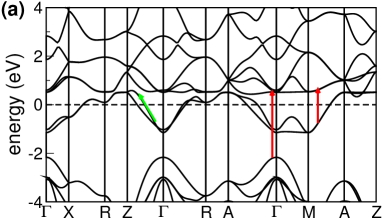
As a first step, we calculate the electronic structure of VO2 for both the rutile and monoclinic phases, whose atomic structures are shown in Fig. 1 and bandstructure plots are displayed in Fig. 2. The R phase [panel (a)] is metallic and characterized by a Fermi level (EF) that overlaps a manyfold of bands with a predominant V3d character. In the octahedral coordination symmetry of rutile crystal, the V3d states are split into -bonded () orbitals, more strongly hybridized with O, and -bonded () orbitals. The bands can be separated into one band crossing the Fermi level, which derives from the overlapping of V3d orbitals along the rutile c-axis, and the remaining subbands located just above EF. The lower-energy bands between -2 and -7 eV have a prominent O2p character, only partially mixed with the V states, and are separated from bands by 1 eV. This matches the experimental values obtained by photoemission spectra Sawatzky1979 ; Verleur1968 and previous theoretical simulations Eyert2011 ; Xiao2014 ; Brito2016 .
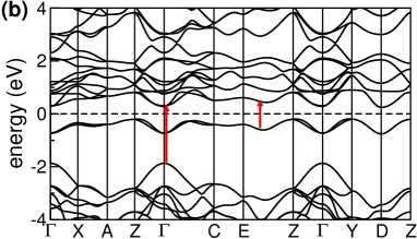
In the monoclinic phase, the crystalline distortion from the tetragonal phase induces an alternate V-V dimerization along the c-axis [Fig. 1(b)], in agreement with the experimental findings RevModPhys.70.1039 ; Qazilbash2007 . The structural symmetry-breaking reflects on the bandstructure [Fig. 2(b)], which exhibits a negative energy shift of the lowest hybridized states to just below EF, resulting in a semiconductor with a narrow indirect bandgap of 0.45 eV between Z and , in agreement with previous experimental Qazilbash2007 ; Koethe2006 ; Sawatzky1979 and theoretical values Brito2016 ; Biermann2005 . More specifically: due to the V-V dimerization the band splits into bonding-antibonding subbands. This causes the lowering of the bonding- band and the upshift of the subbands, opening the gap at the Fermi energy. A multiplet of lower energy O2p-derived bands appears at -2 eV, similar to the R case. Notably, for both phases the inclusion of the Hubbard-like correction pushes the upper V3d and the O2p bands towards higher and lower energy, respectively, leaving the bands close to Fermi energy almost unvaried. This behavior well agrees with the Mott-Peierls character of the M1 phase Qazilbash2007 ; PhysRevB.77.235401 ; Brito2016 .
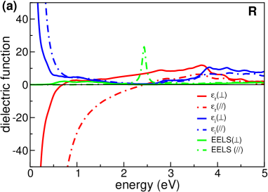
VO2 is highly anisotropic and this reflects on different optical response in the directions parallel or perpendicular to the c-axis of the structure (z direction in Fig. 1). Both parallel and perpendicular components are shown in Fig. 3. The rutile system is characteristic of a Drude-like picture: the divergence at zero energy and the rapid decay of the imaginary part of the dielectric function are representative of the energy damping associated with the dc electrical resistivity of metals. Accordingly, starts strongly negative at low energy and becomes positive at the crossover energy eV. This, along with the condition , results in a peak in the loss function (green curves), which can be directly compared with experiments. The simulated crossover energy well reproduces the experimental value of 2.75 eV detected in EELS measurements Qazilbash2006 . The peak at eV is interpreted as a screened plasmon excitation, typical of transition metals, including Ag and Au rocca1995 . The origin of this plasmonic peak is associated to the coexistence of intra- and interband transitions [see, e.g., green and red arrows in Fig. 2(a)]. Free electron oscillations stem from the intraband transitions of bands that crosses the Fermi level, giving rise to the Drude-tail of for E. At higher excitation energies, the activation of interband transitions between, e.g., occupied and empty states gives a positive contribution to the (negative) Drude component of that becomes positive at the crossover energy . This plasmon is usually labeled as screened as it involves the collective oscillation only of a fraction of the total valence electrons that can be considered as free, the rest being effectively screened by interband transitions. The broad and structured band in spectrum for E 2.5 eV is associated with the optical absorption of the material in the visible range and is due to interband transitions between occupied O2p and unoccupied V3d states. The crossover energy thus identifies two well distinguished optical characters for the material: reflective for and absorptive for .
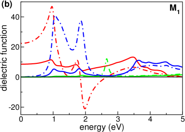
The dielectric function of monoclinic phase has the behavior typical of semiconductors [Fig. 3(b)]: the real part of the dielectric function has finite value at eV, which corresponds to the (parallel and perpendicular) value of the static dielectric constant. The alternated V-V dimerization along the c-axis enhances the differences between the parallel and perpendicular components of the dielectric function. While remains always positive over the entire considered energy range, changes sign in the visible range, exhibiting a typical Lorentz behavior. This generates the appearance of a crossover frequency at E=2.66 eV, which corresponds to a peak in the corresponding loss spectrum. The imaginary parts are dominated by a double peak between 1-2 eV. The lowest energy component corresponds to the onset of the insulating gap. The second major peak at 2.1 eV is the result of larger energy transitions between the states and the lowest conduction band at point.
III.2 Joint-phase mixtures
Although the optical anisotropy is a general condition in uniaxial systems, this is often not sufficient to qualify the intrinsic material as a natural HMM. Following the pioneering work by Qazilbash and coworkers Qazilbash2006 ; Qazilbash2007 ; Qazilbash:2009gr , we considered mixed phase films whose relative semiconductor/metal ratio can be reversibly modified. In particular, starting from room temperature semiconducting system they observed the appearance of metallic puddles at the critical temperature. Puddles enlarge and coalesce as the temperature is further increased to form a complete metallic phase. Provided the incident wavelength is large compared to the size of the metallic inhomogeneities, the mixed system can be described by an effective dielectric function within the EMA.
For a homogeneous disordered systems [Fig. 4(a)] we assumed a Bruggeman mixing model (BMM) Sihvola:1999wv , where the effective dielectric function is given by solving the equation:
| (3) |
where and are the complex dielectric functions of the metal rutile and dielectric monoclinic phase, respectively, calculated from first principles note_metal . In this case, when calculating , the different vector components of the dielectric tensor for each individual R and M1 phase are first averaged over the three spatial directions so as to simulate the random crystal orientations found in a realistic experimental environment. In Eq. (3) the volume fractions of the metallic and insulating phases are given by and , respectively; is a depolarization factor that depends on the geometry of the phases. If we consider an insulating film with evenly spaced, spherical metallic inclusions, the depolarization factor, , is given by 1/3. This is a valid assumption as long as the diameter of each metallic sphere does not exceed the thickness of the film.

The simulated 2D plot of reflectance of the mixed phase metamaterial, as a function of the incoming radiation energy () and the filling fraction () is shown in Fig. 5(a). For and , recovers the semiconducting and metallic behavior of the M1 and R phases, respectively. The most striking feature of the reflectance spectrum is the behavior in an energy window of 0.2 - 1.0 eV. If we focus on a single energy value in this range, we witness the reflectance of the sample transition from perfectly absorbing to reflecting as the percentage of metal is increased. The modulation of is in agreement with experiments that exhibit orders of magnitude shifts in reflectance of a VO2 sample in the near infra-red energy regime as the material undergoes the MIT Krishnamoorthy2014 ; Rensberg2016 ; Kats2012 ; Qazilbash2007 . However, in the comparison with experiment we have to notice that our results are relative to pure VO2 films. All experiments to-date necessitate an underlying substrate that may influence the overall optical properties of the whole VO2/substrate system. Common substrate, such as TiO2 or sapphire, are themselves strongly absorbing at singular wavelengths in THz region. This may explain why experiments have thus far seen near-perfect absorption at only a specific energy value and not in a larger energy range.
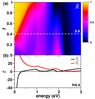
For eV, while there is a point of minimal reflectance in the medium-near IR region for each filling factor, the energy value at which the film demonstrates lowest reflectance is blue-shifted as the metallic component is increased. For the system acts as an effective metallic compound. In the energy range 1.0–2.5 eV the mixture is only partially reflecting for every semiconductor/metal composition with being 30-50% on average. Additionally, there is a point of even lower reflectance for all phase proportions in the visible spectrum, at approximately 2.25 eV. At higher energies, i.e. beyond the crossover frequency of both M1 and R phases, the metamaterial is no more reflecting and the absorption processes become preponderant. Occurrence of metallicity at is confirmed by the plot of the real and imaginary part of the effective dielectric function, shown in Fig. 5(b) for the same value.
The spontaneous arrangement of the metallic puddles in mixed films does not allow to define preferential directions for the effective optical response. However, throughout the spatial control of defects or strain it is possible to fabricate joint-phase metamaterials with periodic sequence of metallic and semiconducting sections. In particular, following the experimental work by Rensberg et al (Ref. [16]), we considered a ridged heterostructure (RHS) of alternating stripes of metallic and semiconducting VO2 material, as shown in Fig. 4b. In this case, we can easily distinguish two components of the dielectric function: the direction parallel () or perpendicular () to the ridges. Starting from the Bruggeman formula [Eq. (3)] and setting the depolarization factors parallel and perpendicular to the ridges equal to and , the effective (complex) dielectric functions are:
| (4) | |||||
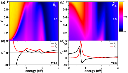
The structural spatial anisotropy of ridged heterostructure clearly reflects on the optical response, as shown in Fig. 6. At low energies (E 0.5 eV), when polarized along the ridges the incoming electric field is perfectly reflected for a range of metal content. Conversely, in the IR-vis range the system is only partially reflecting having , due to interband absorption. As for BMM mixture, the minimum of reflectance is at 2.2 eV for all metallic contents. Completely different is the optical response in the direction perpendicular to the ridges: is generally except for very high metal percentages (80%). In particular, at low energies and low metallic content the material is essentially transparent, in agreement with the experimental findings Rensberg2016 . Nevertheless, since the present theoretical description does not include the effect of the coupling with the lattice vibrations, we do not observe the Reststrahlen band and the modification of reflectance at 11m, as discussed in the original paper Rensberg2016 .
The different reflectivity of RHS is made evident from the comparison of the effective dielectric functions [panels (c),(d)] calculated for , which reproduces the experimental case of Ref. [16]. has the typical fingerprints of a -metal: it is dominated by a Drude-like tail for and by a crossover frequency of at E=0.75 eV, which corresponds to the excitation of a screened plasmon. Notably, with respect to the rutile phase, the plasma frequency is now strongly redshifted. This effect can be ascribed to insertions of the dielectric sections, which reduce the overall free electron density. The imaginary part, , is characterized by an absorption band in the IR-vis region due to many interband transitions, e.g. between occupied or and the states just above the Fermi Level, as pictorially indicated by red arrows in Fig. 2. Along the perpendicular direction, the dielectric function represents a semiconducting system, with converging to the static dielectric constant for . Again, the presence of the metallic component increases the electrostatic screening to result in a higher value of with respect to the M1 phase and in the shrinking of the absorption band that now is singly peaked around E=0.75 eV, i.e. the energy value corresponding to the plasma frequency of the parallel component.
The directional optical response of this ridged structure indicates that ordered joint-phase heterostructures may sustain radiation with hyperbolic dispersion. In order to get deep insight on this point, we considered the standard geometry exploited in the fabrication of HMMs given by the alternate stacking of metallic and dielectric layers [Fig. 4(c)]. Actually, this kind of VO2 structure has not been fabricated, yet. However, the rapid and continuous improvements in the spatially selective control of metallic and semiconducting phases (e.g. checkerboard pattern, ridged and herringbone structures, stacked nanobeams) doi:10.1021/nl903765h ; doi:10.1021/nl103925m ; Kim2016 ; 0957-4484-28-8-085701 make the growth of VO2 layered heterostructures (LHS) very reasonable in the short-medium term.
Assuming the stacking direction as the anisotropy optical axis, the parallel and perpendicular components of the effective dielectric function are given by Poddubny:2013cy :
| (5) | |||||
where and are thicknesses of the metallic and dielectric layers [Fig. 4(c)]. The RHS and the LHS model are formally equivalent as and with .
We analyzed the hyperbolic dispersion condition of VO2 LSHs, plotting the sign function
| (6) |
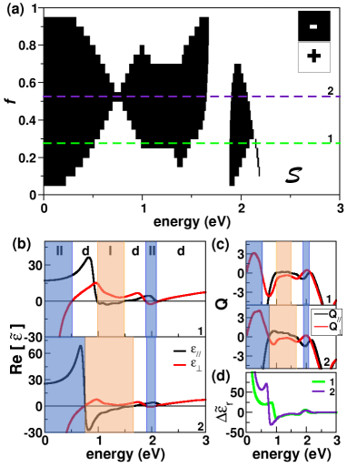
Black areas in Fig. 7(a) identify the regions where the sign function is negative, i.e. where the metamaterial has a hyperbolic behavior: two broad interconnected regions at 0–0.7 and 0.7–1.7 eV; one narrow region at 1.9–2.1 eV. To investigate the characteristics of these regions we select two values of metal content, namely and (labeled 1 and 2, respectively in Fig. 7) and we plot the corresponding parallel and perpendicular components of the dielectric function [panel (b)]. From the comparison between the two panels it follows that each area of panel (a) corresponds to different electrical characteristics. White sections, for which the dielectric functions have the same sign, correspond to an overall dielectric character, being both components of finite and positive. Black areas correspond to distinct hyperbolic types: at lower and higher energies (blue areas in Fig. 7) we see and , which is the definition of type-II HMMs, while in the intermediate region (orange areas) the condition and identifies a type-I HMM. The energy alternation of these electrical behavior depends on the specific metal/semiconductor ratio in the sample. At low metal content (1) the hyperbolic regions are separated by dielectric energy gaps. In case 2, the sample switches from type-II to type-I at E=0.75 eV, where both components are zero (epsilon-near-zero ENZ regime Engheta286 ).
Along the lines of Ref. [6], we define two parameters in order to quantify the hyperbolic character of LHS, namely the quality factor , and the strength of dielectric anisotropy :
| (7) | |||||
with . The results for the key LHS systems 1 and 2 are summarized in Fig. 7(c). Although plotted over the entire energy range 0-3 eV for completeness, the quality factor accounts for the energy losses only along the direction in which the material has a metallic character. Thus, for the perpendicular component it is meaningful in the type-II region (blue area), while for the parallel component in the type-I region (orange area). Systems with hyperbolic character () are considered good HMM if the maximum value of the quality factor is . Both systems satisfy this condition at low energy ( eV): they reach the maximum at 0.3 eV, where (1)=3.1 and (2)=4.1. This qualifies VO2 heterostructures as good type-II HMM materials in the THz and mid-IR regions. At higher energies, despite a formal hyperbolic character of the system, the metal energy loss prevents any realistic application of these LHSs as good metamaterials.
The same conclusion comes from the analysis of the strength of dielectric anisotropy [Fig. 7(d)]. Since the hyperbolic behavior derives from the spatial anisotropy of the optical response, the quality of HMM derives not only from the magnitudes of the constituent dielectric functions, but from their differences or ratios. As the metal ratio in the heterostructure increases, the maximum value of increases and diverges for while its energy position is monotonically redshifted. This corresponds to the fact that for , the real part of the dielectric function in the metal component becomes so negative that there is an impedance mismatch with the other medium. Systems with 20–30 are considered good HMMs Korzeb:2015fv . The complete analysis of our results show that in the case of layered VO2, this condition is reached for , with ranging from mid-IR to THz regions. The strength of dielectric anisotropy also affects the dispersion relation of the radiation that may propagate along the medium, as and define the geometric characteristics of the hyperbolic isosurface equation .
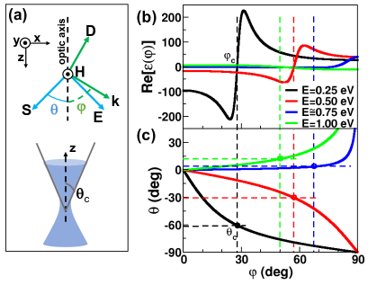
Let us consider the radiation pattern in the case of VO2 LHSs: In general, electromagnetic waves cannot propagate in media with negative permittivity (e.g. metals). In the particular case of HMMs, the condition implies that the system behaves like a metal in one direction and as a dielectric in the other. As a consequence, waves with arbitrarily large wavevectors k may have a propagating nature, while in isotropic materials they become evanescent due to the bound isofrequency contour (a sphere). In this sense, HMMs can be considered as plasmon-polaritonic crystals where the coupled states of light and electron density (i.e. plasmons) give rise to travelling extraordinary (TM) Belov:2003ge waves, known as volume plasmon polaritons (VPP) Zhukovsky:13 ; Ishii:2013er . To characterize these VPPs, we consider the electromagnetic field condition corresponding to the vector diagram shown in Fig. 8(a), where E is the electric-field vector, D is the electric-displacement vector, and S is the Poynting vector. D lays in the principal plain containing both optical axis (aligned along ) and the wavevector. is the angle between the wavevector and the optical axis. In anisotropic materials, the vectors E and D are not usually parallel. An immediate consequence of this is that the Poynting vector S, which points in the direction of energy flow, and wavevector k, directed along the wavefront normal, need not to be parallel.
The spatial anisotropy of HMM can be expressed through an angular dependence of the dielectric function Ishii:2013er :
| (8) |
The condition determines the angular boundary between the metallic and dielectric response of the metamaterial. The critical angle is the direction of the incident radiation that may excite the formation of a travelling plasmon-polariton wave in the system. If we consider the interface with a another dielectric medium (e.g. air), the wavevector at the interface follows Snell’s law. Thus, the angle between the extraordinary wave (i.e. the Poynting vector) and the optical axis is Ishii:2013er . At the critical angle , reduces to the asymptotic expression , and represents the angle of propagation of the VPP along the metamaterial. This means that the plasmon-polariton propagates throughout the volume of the HMM along a cone with axis coincident to the optical axis and angle [Fig. 8(a)]. The number of VPP modes that can be excited depends on the actual number of metal/dielectric layers in the heterostructure. The maximum number of modes in an ideal structure is always one less than the number of metallic layers. However, a real structure always has a maximum wavevector beyond which the VPP modes cannot exist. This happens when the size of the VPP wavevector becomes comparable to the size of the layers comprising the HMM and the modes no longer experience a homogeneous effective medium. The latter is also the validity breakdown of the effective medium approximation. The k wavevector follows a truly hyperbolic surface (i.e. open form) only for the ideal case with zero absorption processes. In the case of real absorbing materials, the isosurface equation reduces to a closed form, whose final dispersion crucially depends on the imaginary part of the dielectric function.
The angular dependence of and the critical angle in the case of VO2 LHSs (=0.5) are shown in Fig. 8(b-c), for different values of the incoming radiation energy. In the low energy region ( eV), where the system has a type-II character (black and red lines), the absolute value of decreases, while shifts to larger angles ( and ) as the value of is increased [panel (b)]. The dielectric functions look like a single dipolar resonance with a high value of the imaginary components (not shown). The corresponding negative critical angles [ and , panel (c)] indicate the propagation of lateral backward wave with respect to the interface without negative refraction Belov:2003ge . At eV the real part of is zero and is indefinite. Approaching this critical value in the ENZ region, e.g. eV (blue line), crosses the zero at . The corresponding critical angle is very small, imparting an extreme conical focusing to the propagation wave. At eV the system has a type-I character (green line) with a small valued dielectric function, typical of dielectric-like HMMs. In this case the critical angle is small and positive, which corresponds to a standard positive wave refraction within a collimated propagation cone, and could be exploited for applications in hyperlenses.
IV Conclusion
We presented a first principles investigation of the optical properties of VO2 and used EMA to determine the properties of mixed-phase metamaterials obtained by combining different phases of the same VO2 compound, i.e. without the introduction of other different media, to form structured materials with original and tunable optoelectronic properties and (in certain cases) with highly anisotropic permittivity. Our results complement and agree with experiments performed on both disordered mixtures and ordered ridged structures. Furthermore, we demonstrated the possibility to use a variable amount of metallic VO2 content in device applications where it is necessary to control the optical properties at a target wavelength.
Finally, we investigated the hyperbolic behavior and the plasmonic characteristics of stacked VO2 heterostructures, a still unexplored possibility made feasible by the unique properties of this phase change compound. The possibility to realize joint-phase mixtures allows one to combine the optical constants of single phases to form a ready-made metamaterial with unforeseen properties. Indeed, this combines the structural tunability typical of artificial HMMs with reduced intermaterial interfaces typical of natural HMMs, and thus opens the way for a new class of metamaterials with controllable optical properties over a wide energy range (THz to visible).
V Acknowledgments
We thank Thushari Jayasekera for her friendly support and advice. ME acknowledges the Southern Illinois University Study Abroad Program for facilitating international collaboration in addition to the SIU Chancellor’s Scholar Program and Center for Undergraduate Research and Creative Activities (CURCA) for partial financial support.
References
- (1) W. Cai and V. Shalaev, Optical Metamaterials: Fundamentals and Applications, Springer, New York, NY, 2010.
- (2) S. A. Ramakrishna, Rep. Progr. Phys. 68, 449 (2005).
- (3) A. Poddubny, I. Iorsh, P. Belov, and Y. Kivshar, Nature Phot. 7, 958 (2013).
- (4) A. J. Hoffman, L. Alekseyev, S. S. Howard, K. J. Franz, D. Wasserman, V. A. Podolskiy, E. E. Narimanov, D. L. Sivco, and C. Gmachl, Nature Materials 6, 946 (2007).
- (5) Z. Jacob, L. V. Alekseyev, and E. Narimanov, Opt. Expr. 14, 8247 (2006).
- (6) S. Ishii, A. V. Kildishev, E. Narimanov, V. M. Shalaev, and V. P. Drachev, Laser & Phot. Rev. 7, 265 (2013).
- (7) C. L. Cortes, W. Newman, S. Molesky, and Z. Jacob, J. Optics 14, 063001 (2012).
- (8) E. E. Narimanov and A. V. Kildishev, Nature Phot. 9, 214 (2015).
- (9) J. Sun, N. M. Litchinitser, and J. Zhou, ACS Photonics 1, 293 (2014).
- (10) K. Korzeb, M. Gajc, and D. A. Pawlak, Opt. Exp. 23, 25406 (2015).
- (11) M. Imada, A. Fujimori, and Y. Tokura, Rev. Mod. Phys. 70, 1039 (1998).
- (12) D. Kucharczyk and T. Niklewski, J. Appl. Cryst. 12, 370 (1979).
- (13) Y. Abate, R. E. Marvel, J. I. Ziegler, S. Gamage, M. H. Javani, M. I. Stockman, and R. F. Haglund, Sci. Rep. 5, 13997 (2015).
- (14) S. Cueff, D. Li, Y. Zhou, F. J. Wong, J. A. Kurvits, S. Ramanathan, and R. Zia, Nature Commun. 6, 8636 (2015).
- (15) F. Menges, M. Dittberner, L. Novotny, D. Passarello, S. S. P. Parkin, M. Spieser, H. Riel, and B. Gotsmann, Appl. Phys. Lett. 108 (2016).
- (16) J. Rensberg, S. Zhang, Y. Zhou, A. S. McLeod, C. Schwarz, M. Goldflam, M. Liu, J. Kerbusch, R. Nawrodt, S. Ramanathan, D. N. Basov, F. Capasso, C. Ronning, and M. A. Kats, Nano Lett. 16, 1050 (2016).
- (17) H. N. S. Krishnamoorthy, Y. Zhou, S. Ramanathan, E. Narimanov, and V. M. Menon, Appl. Phys. Lett. 104, 2012 (2014).
- (18) Z. Chen, X. Wang, Y. Qi, S. Yang, J. A. N. T. Soares, B. A. Apgar, R. Gao, R. Xu, Y. Lee, X. Zhang, J. Yao, and L. W. Martin, ACS Nano 10, 10237 (2016).
- (19) Q.-Y. Wen, H.-W. Zhang, Q.-H. Yang, Y.-S. Xie, K. Chen, and Y.-L. Liu, Appl. Phys. Lett. 97, 021111 (2010).
- (20) M. Liu, H. Y. Hwang, H. Tao, A. C. Strikwerda, K. Fan, G. R. Keiser, A. J. Sternbach, K. G. West, S. Kittiwatanakul, J. Lu, S. A. Wolf, F. G. Omenetto, X. Zhang, K. A. Nelson, and R. D. Averitt, Nature 487, 345 (2012).
- (21) J. Rensberg, Y. Zhou, S. Richter, C. Wan, S. Zhang, P. Schöppe, R. Schmidt-Grund, S. Ramanathan, F. Capasso, M. A. Kats, and C. Ronning, Phys. Rev. Appl. 8, 014009 (2017).
- (22) E. Strelcov, A. Ievlev, A. Belianinov, A. Tselev, A. Kolmakov, and S. V. Kalinin, Sci. Rep. 6, 29216 (2016).
- (23) S. Savo, Y. Zhou, G. Castaldi, M. Moccia, V. Galdi, S. Ramanathan, and Y. Sato, Phys. Rev. B 91, 1 (2015).
- (24) Y. Wang, J. Zhu, W. Yang, T. Wen, M. Pravica, Z. Liu, M. Hou, Y. Fei, L. Kang, Z. Lin, C. Jin, and Y. Zhao, Natures Commun. 7, 12214 (2016).
- (25) S. Zhang, J. Y. Chou, and L. J. Lauhon, Nano Lett. 9, 4527 (2009).
- (26) M. A. Kats, D. Sharma, J. Lin, P. Genevet, R. Blanchard, Z. Yang, M. M. Qazilbash, D. N. Basov, S. Ramanathan, and F. Capasso, Appl. Phys. Lett. 101 (2012).
- (27) M. M. Qazilbash, M. Brehm, B.-G. Chae, P.-C. Ho, G. O. Andreev, B.-J. Kim, S. J. Yun, A. V. Balatsky, M. B. Maple, F. Keilmann, H.-T. Kim, and D. N. Basov, Science 318, 1750 (2007).
- (28) W. H. Brito, M. C. O. Aguiar, K. Haule, and G. Kotliar, Phys. Rev. Lett. 117, 056402 (2016).
- (29) C. Weber, D. D. O’Regan, N. D. M. Hine, M. C. Payne, G. Kotliar, and P. B. Littlewood, Phys. Rev. Lett. 108, 1 (2012).
- (30) V. Eyert, Phys. Rev. Lett. 107, 016401 (2011).
- (31) R. Yahiaoui and H. H. Ouslimani, J. Appl. Phy. 122, 093104 (2017).
- (32) V. Galitski and Y. B. Kim, Phys. Rev. Lett. 99, 266403 (2007).
- (33) M. Gatti, F. Sottile, and L. Reining, Phys. Rev. B 91, 195137 (2015).
- (34) A. Continenza, S. Massidda, and M. Posternak, Phys. Rev. B 60, 15699 (1999).
- (35) M. M. Qazilbash, M. Brehm, G. O. Andreev, A. Frenzel, P. C. Ho, B.-G. Chae, B.-J. Kim, S. J. Yun, H.-T. Kim, A. V. Balatsky, O. G. Shpyrko, M. B. Maple, F. Keilmann, and D. N. Basov, Phys. Rev. B 79, 075107 (2009).
- (36) S. V. Zhukovsky, O. Kidwai, and J. E. Sipe, Opt. Exp. 21, 14982 (2013).
- (37) P. Giannozzi, S. Baroni, N. Bonini, M. Calandra, R. Car, C. Cavazzoni, D. Ceresoli, G. L. Chiarotti, M. Cococcioni, I. Dabo, A. Dal Corso, S. de Gironcoli, S. Fabris, G. Fratesi, R. Gebauer, U. Gerstmann, C. Gougoussis, A. Kokalj, M. Lazzeri, L. Martin-Samos, N. Marzari, F. Mauri, R. Mazzarello, S. Paolini, A. Pasquarello, L. Paulatto, C. Sbraccia, S. Scandolo, G. Sclauzero, A. P. Seitsonen, A. Smogunov, P. Umari, and R. M. Wentzcovitch, J. Phys.: Condens. Matter. 21, 395502 (2009).
- (38) B. Xiao, J. Sun, A. Ruzsinszky, and J. P. Perdew, Phys. Rev. B 90, 085134 (2014).
- (39) L. A. Agapito, S. Curtarolo, and M. Buongiorno Nardelli, Phys. Rev. X 5, 1 (2015).
- (40) P. Gopal, M. Fornari, S. Curtarolo, L. A. Agapito, L. S. I. Liyanage, and M. Buongiorno Nardelli, Phys. Rev. B 91, 245202 (2015).
- (41) A. Calzolari and M. Buongiorno Nardelli, Sci. Rep. 3, 2999 (2013).
- (42) A. Calzolari, A. Ruini, and A. Catellani, ACS Phot. 1, 703 (2014).
- (43) A. H. Sihvola, Electromagnetic Mixing Formulas and Applications, IET, London, United Kingdom, 1999.
- (44) D. Sawatzky, G. A., Post, Phys. Rev. B 20 (1979).
- (45) H. W. Verleur, A. S. Barker, and C. N. Berglund, Phys. Rev. 172, 788 (1968).
- (46) T. C. Koethe, Z. Hu, M. W. Haverkort, C. Schler-Langeheine, F. Venturini, N. B. Brookes, O. Tjernberg, W. Reichelt, H. H. Hsieh, H. J. Lin, C. T. Chen, and L. H. Tjeng, Phys. Rev. Lett. 97, 1 (2006).
- (47) S. Biermann, A. Poteryaev, A. I. Lichtenstein, and A. Georges, Phys. Rev. Lett. 94, 1 (2005).
- (48) B.-J. Kim, Y. W. Lee, S. Choi, J.-W. Lim, S. J. Yun, H.-T. Kim, T.-J. Shin, and H.-S. Yun, Phys. Rev. B 77, 235401 (2008).
- (49) M. M. Qazilbash, K. S. Burch, D. Whisler, D. Shrekenhamer, B. G. Chae, H. T. Kim, and D. N. Basov, Phys. Rev. B 74, 1 (2006).
- (50) M. Rocca, Surf. Sci. Rep. 12, 1 (1995).
- (51) Due to the correlated nature of VO2, at early stage after the MIT transition the optical behavior of metallic puddles might be different from the those of pure rutile ones.Qazilbash2007 Here we did not consider these modifications and we assumed the rutile dielectric function as the ingredient of the mixing phase, for any metal content.
- (52) A. C. Jones, S. Berweger, J. Wei, D. Cobden, and M. B. Raschke, Nano Lett. 10, 1574 (2010).
- (53) S. Zhang, I. S. Kim, and L. J. Lauhon, Nano Lett. 11, 1443 (2011).
- (54) M. W. Kim, S. S. Ha, O. Seo, D. Y. Noh, and B. J. Kim, Nano Lett. 16, 4074 (2016).
- (55) C. McGahan, S. Gamage, J. Liang, B. Cross, R. E. Marvel, R. F. Haglund, and Y. Abate, Nanotechnology 28, 085701 (2017).
- (56) N. Engheta, Science 340, 286 (2013).
- (57) P. A. Belov, Microwave and Optical Technology Letters 37, 259 (2003).