Predicted Janus monolayer ZrSSe with enhanced n-type thermoelectric properties compared with monolayer
Abstract
In analogy to transition-metal dichalcogenide (TMD) monolayers, which have wide applications in photoelectricity, piezoelectricity and thermoelectricity, Janus MoSSe monolayer has been successfully synthesized by substituting the top Se atomic layer in by S atoms. In this work, Janus monolayer ZrSSe is proposed by ab initio calculations. For the electron part, the generalized gradient approximation (GGA) plus spin-orbit coupling (SOC) is used as exchange-correlation potential, while GGA for lattice part. Calculated results show that the ZrSSe monolayer is dynamically and mechanically stable, which exhibits mechanical flexibility due to small Young’s modulus. It is found that ZrSSe monolayer is an indirect-gap semiconductors with band gap of 0.60 eV. The electronic and phonon transports of ZrSSe monolayer are investigated by semiclassical Boltzmann transport theory. In n-type doping, the between ZrSSe and monolayers is almost the same due to similar outlines of conduction bands. The p-type of ZrSSe monolayer is lower than that of monolayer, which is due to larger spin-orbit splitting for ZrSSe than monolayer. The room-temperature sheet thermal conductance is 33.6 for ZrSSe monolayer, which is lower than 47.8 of monolayer. Compared to monolayer, the low sheet thermal conductance of ZrSSe monolayer is mainly due to small group velocities and short phonon lifetimes of ZA mode. Considering their and lattice thermal conductivities, the ZrSSe monolayer may have better n-type thermoelectric performance than monolayer. These results can stimulate further experimental works to synthesize ZrSSe monolayer.
pacs:
72.15.Jf, 71.20.-b, 71.70.Ej, 79.10.-n Email:sandongyuwang@163.comI Introduction
Thermoelectric generators with no moving parts are silent, reliable and scalable, having potential applications in energy-related issues q0 ; q1 ; q4 ; q6 . The performance of a thermoelectric device is measured by the thermoelectric material’s dimensionless figure of merit
| (1) |
in which S, , T, and are the Seebeck coefficient, electrical conductivity, working temperature, electronic and lattice thermal conductivities, respectively. Identifying materials with high thermoelectric efficiency is challenging by searching for a high power factor () and/or a low thermal conductivity (), which is due to the conflicting combination of these transport coefficients. For metals or degenerate semiconductor, the S and are given bynew1 :
| (2) |
| (3) |
where , and is the carrier concentration, the effective mass of the carrier and carrier mobility, respectively. It is clearly seen that the S and are oppositely proportional to .
Firstly proposed by Hicks and Dresselhaus in 1993q2 ; q3 , the low-dimensional systems or nanostructures could have much higher values than their bulk counterparts. A large variety of two-dimensional (2D) monolayers beyond graphene have been predicted in theory, or synthesized experimentally, such as TMDq7 , Janus TMDq7-1 , group IV-VIq8 , group-VAq9 ; q10 , group-IVq11 monolayers and so on . The heat transports of these 2D monolayers have been widely investigated theoretically or experimentally.
The thermoelectric properties of (M=Mo or W; X=S or Se), orthorhombic group IV-VI (A=Ge or Sn; B=S or Se), As, Sb, Bi, , and ATeI (A=Sb or Bi) monolayers have been systematically investigated theoreticallyq12 ; q15 ; q16 ; q16-1 ; q21 ; q22 ; q14 ; q14-1 ; q14-2 ; q14-3 . For monolayer , the S of 30 mV/K has been reported experimentllyq13 . The phonon transport properties of group-IV, ZnO, GaN and SbAs monolayers have been systematically investigated from ab initio calculationsq23 ; q24 ; q25 ; q26 . Strain dependent phonon transports of 2D Penta-Structures, antimonene, silicene, germanene and stanene have been studied by solving the phonon Boltzmann transport equationq27-1 ; q27-2 ; q27-3 .
Recently, the Janus monolayer MoSSe, breaking inversion and mirror symmetry , has been confirmed by means of scanning transmission electron microscopy and energy-dependent X-ray photoelectron spectroscopyq7-1 . Based on ab initio calculations, the large in-plane and vertical piezoelectricity in Janus TMD MXY (M =Mo or W, X/Y = S, Se or Te) has been predicted, which reveals the potential for utilizing piezoelectric 2D materialsn1 . Electronic and optical properties of pristine and vertical and lateral heterostructures of Janus MoSSe and WSSe monolayers have been reported on the basis of electron-electron self-energy correctionsn2 . The Janus monolayer related with 2H structure TMD has been widely studied, and it is amusing to explore 1T Janus TMD monolayer. The representative 1T TMD is , which has been successfully synthesized experimentallyn3 . The of monolayer is predicted to be much lower than those of (M = Mo or W; X = S or Se) monolayersq8 . Strain-induced enhancement of thermoelectric performance in monolayer has been predicted, based on first-principles calculations combined with the Boltzmann transport theoryn4 .
To further improve thermoelectric performance of monolayer, Janus monolayer ZrSSe is proposed, which can be constructed by substituting the top S atomic layer in by Se atoms. It is found that the ZrSSe monolayer is dynamically and mechanically stable, exhibiting mechanical flexibility. An indirect-gap semiconductor is observed in ZrSSe monolayer, with band gap of 0.60 eV using GGA+SOC. Calculated results show that, in n-type doping, the between ZrSSe and monolayers is almost the same due to similar outlines of conduction bands. The room-temperature sheet thermal conductance (33.6 ) of ZrSSe monolayer, is lower than that (47.8 ) of monolayers, which is mainly due to smaller group velocities and shorter phonon lifetimes of ZA mode. Considering their and , the ZrSSe monolayer may have better n-type thermoelectric performance than monolayer.
The rest of the paper is organized as follows. In the next section, the computational details about electronic structures, electron and phonon transports are given. In the third section, we shall present elastic properties, electronic structures, electron and phonon transports of ZrSSe monolayer. Finally, we shall give our discussions and conclusions in the fourth section.

| Name | |||||
|---|---|---|---|---|---|
| 3.68 | 2.58 | - | 1.12 | 0.09 | |
| ZrSSe | 3.74 | 2.57 | 2.71 | 0.60 | 0.21 |
| Name | |||||
|---|---|---|---|---|---|
| 75.96 | 16.23 | 29.82 | 72.49 | 0.21 | |
| ZrSSe | 68.84 | 14.72 | 27.06 | 65.69 | 0.21 |
| 138.5 | 31.7 | 53.4 | 131.2 | 0.23 | |
| MoSSe | 126.8 | 27.4 | 49.7 | 120.9 | 0.22 |
II Computational detail
The electronic structures of and ZrSSe monolayers are calculated by a full-potential linearized augmented-plane-waves method within the density functional theory (DFT)1 , as implemented in the WIEN2k code 2 . The GGA of Perdew, Burke and Ernzerhof (GGA-PBE)pbe is used as the exchange-correlation functional, and the free atomic position parameters are optimized with a force standard of 2 mRy/a.u.. The SOC is included self-consistently 10 ; 11 ; 12 ; so . The convergence results are determined by using 4000 k-points in the first Brillouin zone (BZ) for the self-consistent calculation, making harmonic expansion up to in each of the atomic spheres, and setting for the plane-wave cut-off. From calculated energy band structures, the electronic transport coefficients are performed through solving Boltzmann transport equations within the constant scattering time approximation (CSTA), as implemented in BoltzTrap codeb . To obtain accurate transport coefficients, the parameter LPFAC is set as 20, and at least 2000 k-points is used in the irreducible BZ for the calculations of energy band structures.
The lattice thermal conductivity is performed by using Phono3py+VASP codespv1 ; pv2 ; pv3 ; pv4 . With the plane-wave-cut-off energy of 500 eV, the GGA-PBEpbe is used for the exchange-correlation functional. The energy convergence criteria is eV. The lattice thermal conductivity is calculated by solving linearized phonon Boltzmann equation with single-mode relaxation time approximation (RTA), as implemented in the Phono3py codepv4 . The lattice thermal conductivity can be attained by the following formula:
| (4) |
where is phonon mode, is the total number of q points sampling BZ, is the volume of a unit cell, and , , is the specific heat, phonon velocity, phonon lifetime. The phonon lifetime can be calculated by phonon linewidth of the phonon mode :
| (5) |
The takes the form analogous to the Fermi golden rule:
| (6) |
in which is the phonon equilibrium occupancy and is the strength of interaction among the three phonons , , and involved in the scattering. Based on the supercell approach with finite atomic displacement of 0.03 , the second (third)-order interatomic force constants (IFCs) can be attained by using a 5 5 1 (3 3 1) supercell with k-point meshes of 2 2 1 (3 3 1). According to the harmonic IFCs, phonon dispersions can be attained by Phonopy packagepv5 . To compute lattice thermal conductivities, the reciprocal spaces of the primitive cells are sampled using the 100 100 1 meshes.
It is noted that, for 2D material, the calculated electrical and thermal conductivities depend on the length of unit cell along z direction2dl . They should be normalized by multiplying , in which is the length of unit cell along z direction, and d is the thickness of 2D material. It is well known that the d is not well defined like graphene. In this work, the =20 is used as . By , the thermal sheet conductance can be attained.
III MAIN CALCULATED RESULTS AND ANALYSIS
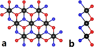
The structure of Janus monolayer ZrSSe is similar to monolayer with the 1T phase, which contains three atomic sublayers with Zr layer sandwiched between S and Se layers. The organized Janus monolayer ZrSSe can be attained by fully replacing one of two S layers with Se atoms in monolayer. Compared with monolayer, the Janus monolayer ZrSSe lacks the reflection symmetry with respect to the central metal Zr atoms. The schematic crystal structure is given in Figure 1, which belongs to the space group of (No.156), being lower than one of monolayer ([No.164]). To avoid spurious interaction, the unit cell is built with the vacuum region of larger than 15 . The optimized lattice constants within GGA-PBE are ==3.74 , which are about 1.6% higher than those of monolayer (==3.68 ). It is found that the bond length of Zr-S between ZrSSe and monolayers is almost the same, but the bond length of Zr-Se in ZrSSe monolayer is longer than that of Zr-S. The related data are listed in Table 1.
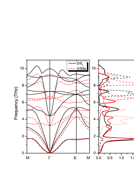
To confirm the dynamical stability, phonon dispersion of Janus monolayer ZrSSe is plotted in Figure 2. It is clearly seen that no imaginary vibrational frequency is observed in the first BZ, which suggests that monolayer ZrSSe is dynamically stable. The mechanical stability of monolayer ZrSSe can be confirmed by calculating the elastic constants. Due to the hexagonal symmetry, there are two independent elastic constants = and , and the =(-)/2. The elastic constants of and ZrSSe monolayers are listed in Table 2, which satisfy the Born criteria of mechanical stability, namely
| (7) |
The 2D Young s moduli in the Cartesian [10] and [01] directions are givenela
| (8) |
The corresponding Poisson’s ratios can be attained by
| (9) |
and the 2D shear modulus is
| (10) |
According to Table 2, the elastic constants, shear modulus, Young’s modulus of ZrSSe monolayer are slightly smaller than ones of monolayer. This indicates that ZrSSe monolayer is more flexible than monolayer due to smaller Young’s modulus. The smaller Young’s modulus may be resulting from the weaker Zr-Se bond strength. The calculated Young’s modulus and Poisson’s ratio of monolayer agree well with previous theoretical valuesrsc , which ensures the reliability of our results. The elastic constants, shear modulus and Young’s modulus of and MoSSe monolayersn1 are also listed in Table 2. Similar to and ZrSSe monolayers, the related elastic quantities of MoSSe monolayer are smaller than ones of monolayer. Compared to MoSSe, the in-plane strain engineering of large magnitude in ZrSSe monolayer can be easily achieved due to small Young’s modulus, which is very important for tuning physical properties of ZrSSe monolayer by strain.
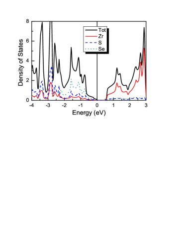
The SOC has important effects on electronic structures and electronic transport coefficients in semiconducting TMD monolayersq14 ; qgsd . Here, GGA+SOC is employed to study energy band structures and electronic transport properties of and ZrSSe monolayers, and their energy band structures are plotted in Figure 3. It is found that both and ZrSSe monolayers are indirect band gap semiconductors with the valence band maximum (VBM) at the point and conduction band minimum (CBM) at the M point. The band gap (0.60 eV) of ZrSSe monolayer is smaller than that (1.12 eV) of monolayer, but the spin-orbit splitting at the point near the Fermi level in the valence bands is larger for ZrSSe monolayer (0.21 eV) than monolayer (0.09 eV). Due to both inversion and time-reversal symmetries, all the bands of monolayer are doubly degenerate. However, It is clearly seen that double degenerate bands of ZrSSe monolayer are removed due to lack of inversion symmetry. From density of states (DOS) of ZrSSe monolayer in Figure 4, the valence bands near the fermi level are composed of S-p and Se-p states, while Zr-d states have main contributions in the conduction bands.
After the energy band structures are completed, the electronic transport coefficients of and ZrSSe monolayers can be attained using CSTA Boltzmann theory. The Seebeck coefficient S, electrical conductivity with respect to scattering time , power factor with respect to scattering time and as a function of doping level using GGA+SOC at room temperature are plotted in Figure 5. The electronic thermal conductivity is connected to the electrical conductivity by the Wiedemann-Franz law:
| (11) |
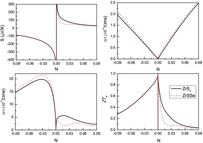
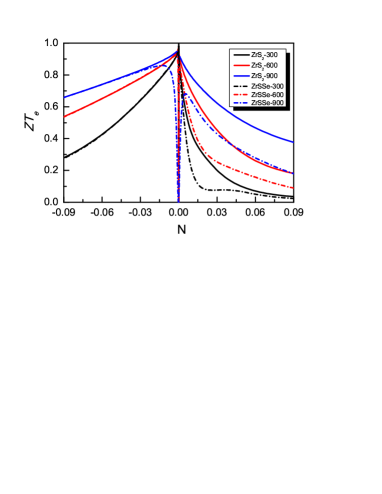
where is the Lorenz number. It is noted that the S is independent of , while electrical conductivity and power factor depend on . The as an upper limit of is also independent of , taking no account of . Within the framework of rigid band approach, the n- or p-type doping can be simulated by simply shifting Fermi level into conduction or valence bands. It is found that n-type S between and ZrSSe monolayers are pretty much the same, which is due to similar profile of conduction bands between and ZrSSe monolayers. However, the p-type S of ZrSSe monolayer is lower than that of monolayer in low doping level, which can be explained by enhanced spin-orbit splitting in the valence bands for ZrSSe monolayer, reducing the strength of orbital degeneracies. The of ZrSSe monolayer is slightly higher than that of monolayer in considered doping level range. For , n-type doping of ZrSSe monolayer is higher than that of monolayer, while p-type doping is opposite. The relation of between and ZrSSe monolayers is the same with that of S. The temperature dependence of of and ZrSSe monolayers is also plotted in Figure 6. It is clearly seen that the n-type between and ZrSSe monolayers is almost the same in considered doping and temperature range except low doping at 900 K. If of ZrSSe monolayer was lower than that of monolayer, the ZrSSe monolayer would have better n-type thermoelectric properties than .
Next, we investigate the phonon transports of and ZrSSe monolayers. Firstly, the phonon dispersions of are also plotted in Figure 2, together with atomic partial DOS, which are consistent with available theoretical resultsn4 . The phonon dispersions determine the allowed three-phonon scattering processes. Due to three atoms in the unit cell of and ZrSSe monolayers, there are 3 acoustic and 6 optical phonon branches. The longitudinal acoustic (LA) and transverse acoustic (TA) branches are linear near the point, while the z-direction acoustic (ZA) branch is quadratic, which shares general features of 2D materialsq12 ; q15 ; q16 ; q16-1 ; q21 ; q22 ; q14 ; q14-1 ; q27-1 ; q27-2 ; q27-3 . Compared to monolayer, the phonon dispersions of TA and LA modes of ZrSSe monolayer become softened, while ZA mode has little change. From to ZrSSe monolayer, the whole optical branches move toward lower energy. These mean that ZrSSe monolayer has smaller group velocities than monolayer. Unlike monolayernew2 , no acoustic-optical (a-o) gap is observed for both and ZrSSe monolayers, which produce important effects on acoustic+acousticoptical (aao) scattering. For monolayer, the optical modes are mainly from S vibrations, while the acoustic branches are due to the vibrations of Zr. For ZrSSe monolayer, the high-frequency optical modes are mainly due to S vibrations, while the low-frequency optical and acoustic branches are due to the vibrations of Zr and Se atoms.
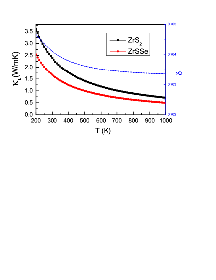
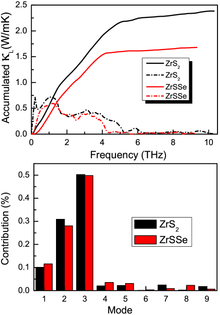
Based on harmonic and anharmonic IFCs, the intrinsic lattice thermal conductivities of and ZrSSe monolayers as a function of temperature are plotted in Figure 7, along with (ZrSSe)/(). For both cases, the follows a with the increasing temperature, which is due to enhanced phonon-phonon scattering. At 300 K, the lattice thermal conductivity is 2.39 for monolayer and 1.68 for ZrSSe monolayer with the same thickness 20 . The thermal sheet conductance can be used to make fair comparison for thermal transport properties of 2D materials2dl , and the corresponding thermal sheet conductance is 47.8 for monolayer and 33.6 for ZrSSe monolayer. In the temperature range investigated, the thermal conductivities of ZrSSe monolayer are about 70% of ones of monolayer. Combining with , ZrSSe monolayer may have better thermoelectric properties than monolayer in n-type doping. For both and ZrSSe monolayers, the accumulated lattice thermal conductivities, the derivatives and the contribution of each phonon mode to the total lattice thermal conductivity are shown in Figure 8. It is clearly seen that the three acoustic phonon branches contribute mostly to the lattice thermal conductivity, around 91.26% for monolayer and 89.38% for ZrSSe monolayer. It is found that the contribution gradually increases from ZA to TA to LA branch in acoustic branches, about 10% for ZA branch, 30% for TA branch and 50% for LA branch.
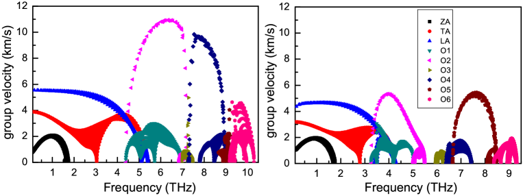
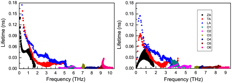
To investigate the origin of lower for ZrSSe monolayer than monolayer, the mode level phonon group velocities and lifetimes are plotted in Figure 9 and Figure 10. The group velocities can be calculated by phonon dispersions from second-order harmonic IFCspv4 . The three-phonon scattering rate can be calculated by third-order anharmonic IFCs, and then the phonon lifetimes can be attainedpv4 . Due to quadratic dispersion of ZA branch near the point, the group velocities of ZA branch are smaller than ones of LA and TA branches. The largest group velocity of monolayer near point is 0.84 for ZA, 3.89 for LA, and 5.54 for TA. For ZrSSe monolayer, the corresponding value is 1.06 , 3.20 and 4.37 . It is found that group velocities of ZA branch between and ZrSSe monolayers are almost the same. For other branches, it is clearly seen that most of group velocities are lower for ZrSSe monolayer than monolayer, which can give rise to decreasing lattice thermal conductivity. These can be explained by phonon softening, which leads to lower group velocity for ZrSSe monolayer than monolayer. On the other hand, the most phonon lifetimes of ZrSSe monolayer for ZA branch are shorter than ones of monolayer, which will benefit the low lattice thermal conductivity. The separation between ZA acoustic branch and optical phonon branches is smaller for ZrSSe monolayer than monolayer, which leads to much more frequent scattering between ZA acoustic modes and optical modes, resulting in shorter phonon lifetimes. Compared to monolayer, the lower of ZrSSe monolayer is mainly due to smaller group velocities and shorter phonon lifetimes of ZA mode.
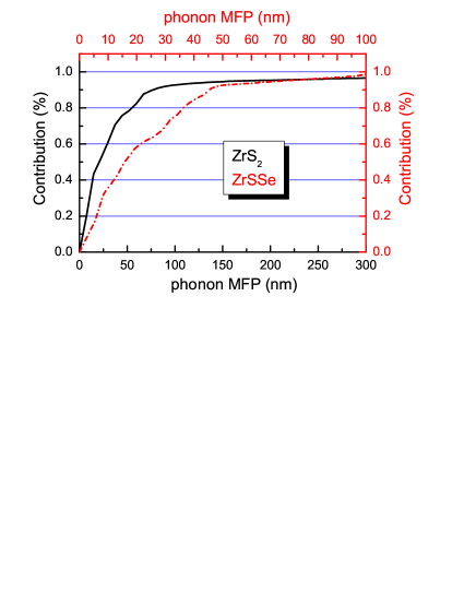
The cumulative lattice thermal conductivity with respect to phonon mean free paths (MFP) can provide information about the contributions of phonons with different MFP to the total thermal conductivity. At room temperature, the cumulative lattice thermal conductivity divided by total lattice thermal conductivity of and ZrSSe monolayers with respect to phonon MFP are plotted in Figure 11. For (ZrSSe) monolayer, phonons with MFP smaller than 55 (37) nm contribute around 80% to total lattice thermal conductivity. This is consistent with lower lattice thermal conductivity for ZrSSe monolayer than monolayer. The stronger intrinsic phonon scattering for ZrSSe monolayer than monolayer can induce lower lattice thermal conductivity by causing phonons to have shorter MFP.
IV Discussions and Conclusion
Recently, the sandwiched S-Mo-Se structure (Janus MoSSe monolayer) has been synthesized by fully replacing the top Se layers with S atoms within monolayerq7-1 . The MoSSe and ZrSSe monolayers have the same space group of (No.156), but the different stacking of S and Se sublayers leads to two crystal structures, namely 1T structure (ZrSSe) and 2H structure (MoSSe), which is due to different ionicity. From Figure 12, the indirect gap of ZrSSe monolayer (0.60 eV) is very smaller than direct gap of MoSSe monolayer(1.47 eV). However, near the Fermi level, the spin-orbit splitting of ZrSSe monolayer (0.21 eV) at the point in the valence bands is larger than that of MoSSe monolayer (0.17 eV) at the K point. The predicted elastic stiffness coefficient of Janus MoSSe monolayer is 126.8 N/m for , 27.4 N/m for n1 , which are larger than ones of ZrSSe monolayer (=68.8 N/m, =14.7 N/m). Compared to MoSSe monolayer, ZrSSe monolayer is more flexible with smaller elastic stiffness coefficients, and the increased flexible nature makes ZrSSe monolayer to be a good choice for large magnitude strain control.
Strain is a very effective method to tune electronic structures, topological and transport properties of 2D materialsq27-1 ; q27-2 ; q27-3 ; n4 ; t9 . Indirect-to-direct band gap transition of monolayer by strain has been predicted by first-principles calculationsrsc , and the band structure can be remarkably modified. For monolayer, the greatly enhanced thermoelectric performance caused by the biaxial tensile strain has been predicted by first-principles calculations combined with the Boltzmann transport theoryn4 . It is found that tensile strain can increase the Seebeck coefficient of monolayer by bands converge, and decrease the lattice thermal conductivity by reducing group velocities of the TA and LA modes. For bulk , the enhanced thermoelectric performance, caused by strain, has also been predicted by ab initio calculations and semiclassical Boltzmann transport theory, which is due to convergence of separate orbitsnew3 . The ZrSSe and monolayers have similar elastic stiffness coefficients, electronic structures and phonon behaviour, so it is possible to improve thermoelectric performance of ZrSSe monolayer by strain engineering.
In summary, using first-principles calculations and semiclassical Boltzmann transport theory, we investigate the stability, mechanical, electronic and transport properties of ZrSSe monolayer. It is proved that ZrSSe monolayer is dynamically and mechanically stable by phonon dispersion and Born criteria of mechanical stability. The ZrSSe monolayer is an indirect gap semiconductor with remarkable spin-orbit splitting. It is found that n-type between ZrSSe and monolayers is almost the same due to identical Seebeck coefficient. However, the of ZrSSe monolayer is lower than that of monolayer, which is due to lower group velocities and shorter phonon lifetimes of ZA phonon mode for ZrSSe monolayer than monolayer. Therefore, the ZrSSe monolayer may have better n-type thermoelectric performance than monolayer. The n-type doping of the ZrSSe monolayer can be realized by adsorption of small molecules, substituting site atoms and electrolyte gatingnew4 ; new5 ; new6 . The ZrSSe monolayer is a potential candidate for thermoelectric application, and our works can stimulate further experimental works to synthesize ZrSSe monolayer.

Acknowledgements.
This work is supported by the National Natural Science Foundation of China (Grant No.11404391). We are grateful to the Advanced Analysis and Computation Center of CUMT for the award of CPU hours to accomplish this work.References
- (1) T. M. Tritt and M. A. Subramanian, MRS Bulletin 31, 188 (2006).
- (2) G. J. Snyder and E. S. Toberer, Nature Materials 7, 105 (2008).
- (3) A. J. Minnich, M. S. Dresselhaus, Z. F. Ren and G. Chen, Energy Environ. Sci. 2, 466 (2009).
- (4) T. C. Harman, P. J. Taylor, M. P. Walsh and B. E. LaForge, Science 297, 2229 (2002).
- (5) M. Cutler, J. F. Leavy, and R. L. Fitzpatrick, Phys. Rev. 133, A1143 (1964).
- (6) L. D. Hicks and M. S. Dresselhaus, Phys. Rev. B 47, 12727 (1993).
- (7) L. D. Hicks and M. S. Dresselhaus, Phys. Rev. B 47, 16631(R) (1993).
- (8) M. Chhowalla, H. S. Shin, G. Eda, L. J. Li, K. P. Loh and H. Zhang, Nature Chemistry 5, 263 (2013).
- (9) A. Y. Lu, H. Y. Zhu, J. Xiao et al., Nature Nanotechnology 12, 744 (2017).
- (10) R. X. Fei, W. B. Li, J. Li and L. Yang, Appl. Phys. Lett. 107, 173104 (2015).
- (11) S. L. Zhang et al., Angew. Chem. 128, 1698 (2016).
- (12) J. P. Ji et al., Nat. Commun. 7, 13352 (2016).
- (13) S. Balendhran, S. Walia, H. Nili, S. Sriram and M.Bhaskaran, small 11, 640 (2015).
- (14) W. Huang, H. X. Da and G. C. Liang, J. Appl. Phys. 113, 104304 (2013).
- (15) G. Qin, Z. Qin, W. Fang, L. Zhang, S. Yue, Q. Yan, M. Hu and G. Su, Nanoscale 8, 11306 (2016).
- (16) S. D. Guo and Y. H. Wang, J. Appl. Phys. 121, 034302 (2017).
- (17) D. C. Zhang, A. X. Zhang, S. D. Guo and Y. F. Duan, RSC Adv. 7, 24537 (2017).
- (18) L. M. Sandonas,D. Teich, R. Gutierrez, T. Lorenz, A. Pecchia, G. Seifert and G. Cuniberti, J. Phys. Chem. C 120, 18841 (2016).
- (19) L. Cheng, H. J. Liu, X. J. Tan, J. Zhang, J. Wei, H. Y. Lv, J. Shi and X. F. Tang, J. Phys. Chem. C 118, 904 (2014).
- (20) S. D. Guo, J. Mater. Chem. C 4, 9366 (2016).
- (21) S. D. Guo, A. X. Zhang and H. C. Li, Nanotechnology 28, 445702 (2017).
- (22) G. P. Li, K. L. Yao and G. Y. Gao, Nanotechnology 29, 015204 (2018).
- (23) G. P. Li, G. Q. Ding and G. Y. Gao, J. Phys.: Condens. Matter 29, 015001 (2017).
- (24) J. Wu et al. Nano Lett. 14, 2730 (2014).
- (25) B. Peng, H. Zhang, H. Z. Shao, Y. F. Xu, G. Ni, R. J. Zhang and H. Y. Zhu, Phys. Rev. B 94, 245420 (2016).
- (26) H. M. Wang, G. Z. Qin, G. J. Li, Q. Wang and M. Hu, Phys. Chem. Chem. Phys. 19, 12882 (2017).
- (27) Z. Z. Qin, G. Z. Qin, X. Zuo, Z. H. Xiong and M. Hu, Nanoscale 9, 4295 (2017).
- (28) S. D. Guo and J. T. Liu, Phys. Chem. Chem. Phys. 19, 31982 (2017).
- (29) Y. D. Kuang, L. Lindsay, S. Q. Shic and G. P. Zheng, Nanoscale 8, 3760 (2016).
- (30) H. K. Liu, G. Z. Qin, Y. Lin and M. Hu, Nano Lett. 16, 3831 (2016).
- (31) A. X. Zhang, J. T. Liu, S. D. Guo and H. C. Li, Phys. Chem. Chem. Phys. 19, 14520 (2017).
- (32) L. Dong, J. Lou and V. B. Shenoy, ACS Nano 11, 8242 (2017).
- (33) F. P. Li, W. Wei, P. Zhao, B. B. Huang and Y. Dai, J. Phys. Chem. Lett. 8, 5959 (2017).
- (34) Z. Zeng, Z. Yin, X. Huang, H. Li, Q. He, G. Lu, F. Boey and H. Zhang, Angew. Chem., Int. Ed. 50, 11093 (2011).
- (35) H. Y. Lv, W. J. Lu, D. F. Shao, H. Y. Lub and Y. P. Sun, J. Mater. Chem. C 4, 4538 (2016).
- (36) P. Hohenberg and W. Kohn, Phys. Rev. 136, B864 (1964); W. Kohn and L. J. Sham, Phys. Rev. 140, A1133 (1965).
- (37) P. Blaha, K. Schwarz, G. K. H. Madsen, D. Kvasnicka and J. Luitz, WIEN2k, an Augmented Plane Wave + Local Orbitals Program for Calculating Crystal Properties (Karlheinz Schwarz Technische Universität Wien, Austria) 2001, ISBN 3-9501031-1-2
- (38) J. P. Perdew, K. Burke and M. Ernzerhof, Phys. Rev. Lett. 77, 3865 (1996).
- (39) A. H. MacDonald, W. E. Pickett and D. D. Koelling, J. Phys. C 13, 2675 (1980).
- (40) D. J. Singh and L. Nordstrom, Plane Waves, Pseudopotentials and the LAPW Method, 2nd Edition (Springer, New York, 2006).
- (41) J. Kunes, P. Novak, R. Schmid, P. Blaha and K. Schwarz, Phys. Rev. B 64, 153102 (2001).
- (42) D. D. Koelling, B. N. Harmon, J. Phys. C Solid State Phys. 10, 3107 (1977).
- (43) G. K. H. Madsen and D. J. Singh, Comput. Phys. Commun. 175, 67 (2006).
- (44) G. Kresse, J. Non-Cryst. Solids 193, 222 (1995).
- (45) G. Kresse and J. Furthmller, Comput. Mater. Sci. 6, 15 (1996).
- (46) G. Kresse and D. Joubert, Phys. Rev. B 59, 1758 (1999).
- (47) A. Togo, L. Chaput and I. Tanaka, Phys. Rev. B 91, 094306 (2015).
- (48) A. Togo, F. Oba, and I. Tanaka, Phys. Rev. B 78, 134106 (2008).
- (49) X. F. Wu, V. Varshney et al., Chem. Phys. Lett. 669, 233 (2017).
- (50) R. C. Andrew, R. E. Mapasha, A. M. Ukpong and N. Chetty, Phys. Rev. B 85, 125428 (2012).
- (51) Y. Li, J. Kang and J. B. Li, RSC Adv. 4, 7396 (2014).
- (52) S. D. Guo and J. L. Wang, Semicond. Sci. Tech. 31, 095011 (2016).
- (53) X. K. Gu and R. G. Yang, Appl. Phys. Lett. 105, 131903 (2014).
- (54) S. L. Zhang, M. Q. Xie, B. Cai, H. J. Zhang, Y. D. Ma, Z. F. Chen, Z. Zhu, Z. Y. Hu, and H. B. Zeng, Phys. Rev. B 93, 245303 (2016).
- (55) G. Q. Ding, J. F. Chen, K. L. Yao and G. Y. Gao, New J. Phys. 19, 073036 (2017).
- (56) D. Kiriya, M. Tosun, P. Zhao, J. S. Kang and A. Javey, J. Am. Chem. Soc. 136, 7853 (2014).
- (57) M. R. Laskar, D. N. Nath, L. Ma et al., Appl. Phys. Lett. 104, 092104 (2014).
- (58) J. T. Ye, Y. J. Zhang, R. Akashi, M. S. Bahramy, R. Arita and Y. Iwasa, Science 338, 1193 (2012).