Electron-Beam Manipulation of Silicon Dopants in Graphene
Abstract
The direct manipulation of individual atoms in materials using scanning probe microscopy has been a seminal achievement of nanotechnology. Recent advances in imaging resolution and sample stability have made scanning transmission electron microscopy a promising alternative for single-atom manipulation of covalently bound materials. Pioneering experiments using an atomically focused electron beam have demonstrated the directed movement of silicon atoms over a handful of sites within the graphene lattice. Here, we achieve a much greater degree of control, allowing us to precisely move silicon impurities along an extended path, circulating a single hexagon, or back and forth between the two graphene sublattices. Even with manual operation, our manipulation rate is already comparable to the state-of-the-art in any atomically precise technique. We further explore the influence of electron energy on the manipulation rate, supported by improved theoretical modeling taking into account the vibrations of atoms near the impurities, and implement feedback to detect manipulation events in real time. In addition to atomic-level engineering of its structure and properties, graphene also provides an excellent platform for refining the accuracy of quantitative models and for the development of automated manipulation.
keywords:
electron microscopy, 2D materials, atom manipulation, nanotechnologynanomat/Q-mat/CESAM, Université de Liège, Institut de Physique, B-4000 Sart Tilman, Liège, Belgium \phone+43-1-427772855
Although single-atom manipulation using scanning probe microscopy was established already 25 years ago 1, 2, it continues to provide impressive technological advances, such as atomic memory arrays, 3 as well as insight into physical phenomena including quantum many-body effects 4, 5. However, only relatively weakly bound surface atoms far below room temperature can typically 6 be affected due to the limited interaction energy with the atomically sharp tip. By contrast, the energetic electrons used in (scanning) transmission electron microscopy (STEM) to image atomic structures can transfer up to tens of electron volts to atoms of light elements such as carbon, allowing the breaking and reforming of covalent bonds. In modern STEM instruments, it is further possible to predominantly direct the electron beam at individual atoms 7 in low-dimensional materials such as single-layer graphene 8.
Silicon heteroatoms, occasionally found in graphene as substitutional impurities 9, 10, have particularly interesting dynamics. In 2014, they were observed to ”jump” through the lattice upon 60 keV electron irradiation 11, with no damage to the structure. First-principles simulations revealed the mechanism of Si-C bond inversions: each electron has a finite chance to transfer just enough out-of-plane kinetic energy to one C neighbor to cause it to exchange places with the Si 11, a rare example of a direct exchange diffusion in a crystalline material 12. In these early findings, the movement was not controlled, but it was clear that this should be possible by purposefully directing the electron irradiation at the desired C neighbor 11, 13.
Recently, some of us achieved the first controlled manipulations 14 by iteratively parking the electron beam for 15 s on top of the C neighbor in the direction the Si should move. These experiments had clear limitations: the Si was moved over just a handful of lattice sites, with unintended double jumps. This lack of control was partly due to the lack of feedback: it was not possible to observe structural changes while the electron beam was parked, resulting in excessive dosing. Dyck et al. recently reported similar manipulations 15, in this case by irradiating a small sub-scan window centered on the C neighbor. However, directional control was rather poor, likely due to dosing of undesired C sites. In a subsequent study, the same group was able to move several nearby Si over a few lattice sites 16.
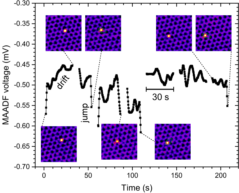
Here, we demonstrate greatly improved manipulation of incidental Si impurities in commercial monolayer graphene, identified by their scattering -contrast 17 and by electron energy loss spectroscopy 10 (Fig. S1). We now reduced the spot irradiation time to 10 s in our Nion UltraSTEM100 instrument operated in near ultra-high vacuum ( mbar) at 60 keV, with a beam current of pA corresponding to a dose rate of 108 e-s-1 in the 1.1 Å diameter spot. For another series of experiments conducted at 55 keV, we further implemented real-time feedback by connecting a Keithley 2000 multimeter to the medium angle annular dark field (MAADF) detector and reading out the raw detector voltage averaged over 150 ms while the beam was parked on the desired atom. These values were read into the Nion Swift microscope control software 18 and used to trigger the acquisition of new image frames. As control logic, an increased intensity corresponds to a successful manipulation event (Si has taken the place of the C, leading to greater scattering), with a threshold of 10% change with respect to the cumulative average of the signal chosen as the trigger condition (see Fig. S2).
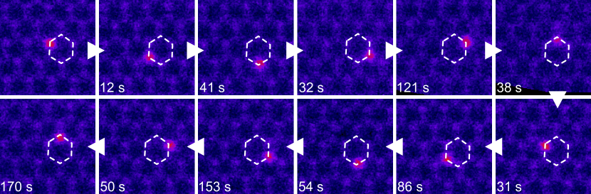
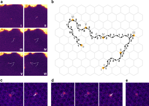
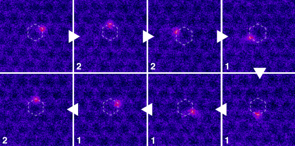
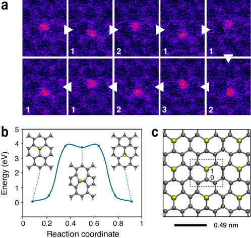
To demonstrate the control we can now achieve, we conducted three types of manipulation experiments at 60 kV. First, we moved a Si atom over a path consisting of 34 lattice jumps precisely in the selected directions, with no undesired motion or double jumps (Fig. 1). Second, instead of extended lateral motion, we moved a Si atom around a graphene hexagon (selected frames from a sequence of 75 jumps, which included several double jumps, are shown in Fig. 2); the probability of just the shown motion being a random walk would be %. Finally, individual Si atoms could be moved back and forth between the two graphene sublattices (selected frames of 67 jumps are shown in Fig. 3a). At 55 keV, we repeated the latter two kinds of experiments, observing very few double jumps due to the now implemented feedback, and collecting further statistical data on the required doses for our theoretical analyses. As shown by these examples, our level of control is sufficient for creating extended structures 19 once the density of impurities can be increased, for example by purposefully implanting them into the lattice 20, 21 or by capturing them in vacancies 16.
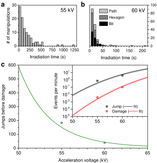
A stacked histogram of all 60 keV manipulation events (Fig. 5a) shows that in most cases (), the required irradiation time is 20 seconds or less (the geometric mean of 15.1 s providing a good estimate for the Poisson expectation value 11), corresponding to a dose of electrons per event and a rate close to 4 jumps per minute (neglecting the frame time of 4.2 s). Remarkably, despite the simplicity of the experimental procedure, this is nearly on par with the state-of-the-art in automated scanning tunneling microscopy-based single-atom manipulation 3. The two outliers with very long irradiation times of 160 and 210 s are unlikely to follow from the same Poisson process 11 as the other manipulation events, but are consistent with 13C atoms (and their frequency, , is very close to the natural carbon isotope abundance). This suggests that graphene grown from isotopically purified precursors 22 would be ideal for further large-scale experiments.
The manipulation rate could be increased by increasing the electron acceleration voltage, but this would also increase the probability of knock-on damage. A lower voltage, on the other hand, would decrease the manipulation rate, but also decrease the probability of damage. Due to their differing threshold energies, the damage probability decreases faster than the probability of a jump as a function of electron energy, which means that the statistically expected number of successful jumps can be increased by lowering the voltage. In our experiments at 55 keV, due to our real-time detector feedback, we were also able to obtain more accurate timing for each jump. In total, we moved individual Si impurities 102 times, with an average rate or jumps per minute, corresponding to an average electron irradiation dose per event of e-. An example of manipulation around a graphene hexagon is shown in Fig. S3. In these series, we observed only one event of knock-on damage, with an apparent rate of min-1 (corresponding to e-). Improving the sharpness of the electron probe would be clearly beneficial: for our expected probe shape 23, we estimate that only 26% of the dose impinges on the area of the targeted C atom. Thus a sharper probe would allow us to increase the manipulation rate of the atom without impacting the relative probability of damage.
We can further compare the observed event doses to a first-principles model that includes the effect of atomic vibrations 24. In our previous estimates, we simply used the pristine graphene phonon dispersion 25 even for systems with impurities 26. Here, we have explicitly calculated the phonon dispersion relations for a graphene super-cell containing 71 C atoms and a single Si impurity and compared this to a monolayer of pure graphene. We use density functional perturbation theory as implemented with the ABINIT software package 27, 28, 29, with norm-conserving pseudo-potentials generated with the ONCVPSP code 30, 31, a plane-wave basis set, and the PBE exchange-correlation functional 32 (the differences with LDA in mean-square velocity are a few percent). After calculating the phonon dispersion, a displacement-weighted phonon density of states is constructed for each atom, and populated with Bose-Einstein thermal factors at 300 K (the temperature of our objective lens close to the sample). With harmonic Gaussian modes, the mean-square velocity is then related directly to the mean-square displacement by the mode frequency 33.
With this method, the out-of-plane mean-square velocity of the C atoms in pristine graphene is around 320 000 m2/s2, as is the mean-square velocity of the nearest-neighbor C atoms to the Si impurity. However, the second nearest neighbors have perceptibly higher velocities, as shown in Fig. S2. Further neighbor velocities decay exponentially back to the pristine value. We attribute the somewhat surprising ‘normal’ values for the first neighbor velocities to a compensation between (1) softer sp3-like bonding with Si (visible in the vibrational frequencies of C-C single, double and triple bonds), and (2) the mass difference, which for a thermalized harmonic oscillator will increase the velocity of the lighter atom. For second neighbors, the bonding returns to sp2 and the pinning effect of the Si-C block generates the higher velocities.
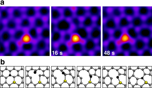
Interestingly, at 55 keV we observed a new type of a dynamical event: a Stone-(Thrower-) Wales 34 bond rotation of the next-nearest C-C bond. This process cannot be activated by an elastic electron impact in pristine graphene at such low voltages 35, whereas at 60 keV, we believe the back-transformation rate 36 to be too fast to image the defect. However, density functional theory based molecular dynamics (DFT/MD) simulations following our established methodology 25 reveal that the local perturbation caused by the impurity allows this process to be activated by impacts with energies between eV on the next-nearest C neighbor to the Si (and for a perpendicular momentum transfer, contrary to the pristine case 35). Combined with the greater velocity of that C atom, this results in a finite event probability even at 55 keV. One of the three such events we observed is shown in Fig. 4, alongside snapshots from an MD simulation elucidating the mechanism.
To compare our model to the manipulation experiments, event cross sections are calculated by integrating the product of a Gaussian velocity distribution (with width parameter ) and the cross section for elastic scattering (in the McKinley-Feshbach approximation 37) for the maximum kinetic energy that the electron can transfer 24 to the nucleus in a momentum and energy conserving collision:
| (1) |
evaluated numerically for all velocities where the maximum transferred energy exceeds the displacement threshold energy (enforced via the Heaviside step function ). is the temperature (here 300 K) and the electron kinetic energy.
We then find displacement threshold energy values that minimize the least squares error of the theoretical curves with our experimental data, plotted in Fig. 5c. From the fits, we obtain a threshold of 13.04 eV for the direct exchange process (DFT: 14.8 eV) 11, whereas the knock-on threshold is 14.44 eV (DFT: 16.9 eV) 11. These discrepancies between experimental and theoretically predicted threshold energies again highlight the inaccuracies of the best available models 26. Since we now include the explicit phonon dispersion for a system with a Si impurity, this shows that the estimate of the displacement threshold energy itself —essentially a description of dynamical bond breaking— needs to be improved before accurate quantitative predictions can be made.
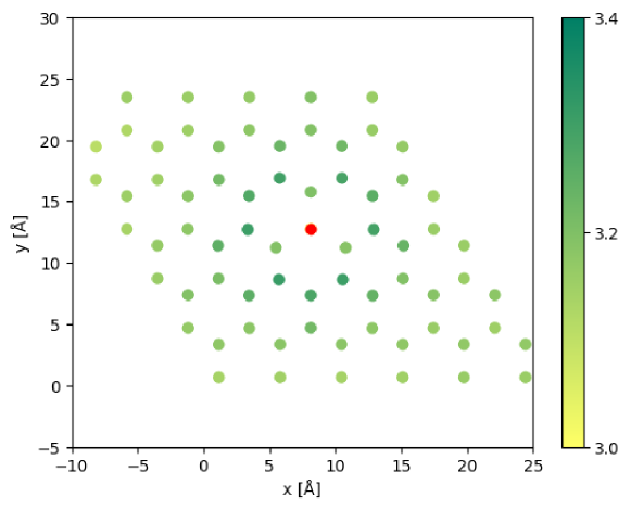
Despite the unavoidable chance of knocking out a C atom, STEM manipulation has several advantages over STM. Because of the strong covalent bonding, the Si migration barrier is very large (close to 4 eV, Fig. 3b, as calculated with the nudged elastic band method 38 within density functional theory using the GPAW software package 39), making any created arrangements stable at temperatures well above room temperature for extended periods of time. In addition, a beam-stable minimum spacing between the Si impurities might be as low as 5 Å (Fig. 3c). If the position of the Si on either of the two sublattices were to encode a single bit value, this would allow a theoretical density as high as 3000 terabits per square inch, i.e., six times higher than the record achieved by manipulating vacancies in a chlorine surface monolayer using STM 3.
Although we emphatically are not proposing that graphene heteroatom bits constitute a practical storage medium in the foreseeable future, there seem to be no fundamental obstacles. At 60 kV, the dose required to cause a jump (flip the bit value) is on the order of e-, whereas the dose falling on the C neighbors of the Si required to record high-quality images is at least two orders of magnitude lower. To simply detect the position of the Si on either of the two sublattices, likely an additional two orders of magnitude lower dose would be sufficient, especially if combined with compressed sensing and computer vision. At 55 kV, due to the greater dose required to move the Si, this difference is one order of magnitude greater still, further reducing the probability of unintended bit flips. It thus appears feasible to both reliably write and read bit values using the same STEM instrument. The manipulation of other heteroatoms 26 along with instrumental advances in beam shaping combined with an optimized acceleration voltage might further improve these capacities.
In conclusion, we have shown how targeted electron irradiation with an Ångström-sized electron probe can reliably move Si impurities through the graphene lattice. The improved degree of control reported here demonstrates the capabilities of scanning transmission electron microscopy as a capable tool for single-atom manipulation in covalently bound materials. Although all atoms in graphene are surface atoms, its impurities are much stronger bound than the surface adatoms or vacancies that can be manipulated with scanning probe techniques, resulting in inherent temperature stability. Furthermore, very recent experiments on manipulating impurities within bulk silicon have provided the first evidence for the applicability of this technique also in three-dimensional crystals 40. Nonetheless, graphene remains highly suited for refining the accuracy of quantitative models and the development of automated manipulation. Optimization of the feedback parameters and the implementation of drift compensation will enhance our capabilities further, to be followed by structure recognition 41 and software-controlled beam re-positioning as the next steps towards full automation.
Supporting Information
Figures S1-S4: EELS spectrum of a Si substitution, MAADF detector feedback time series, example manipulation sequence at 55 keV, and the calculated out-of-plane mean-square velocities of the graphene supercell with a Si impurity. Unprocessed electron microscopy image stacks of the manipulation experiments are provided as open data in Ref. 42.
T.S. and M.T. acknowledge the Austrian Science Fund (FWF) project P 28322-N36 for funding. T.S. was also supported by the European Research Council (ERC) Grant No. 756277-ATMEN, and acknowledges the Vienna Scientific Cluster for computer time. A.M., C.M., and J.C.M. were supported by the ERC Grant No. 336453-PICOMAT. J.K. was supported by the FWF project I 3181-N36 and the Wiener Wissenschafts-, Forschungs- und Technologiefonds (WWTF) project MA14-009. N.A.P was supported by the Research Council of Norway through the Frinatek program and both N.A.P and M.J.V. are supported by the Belgian Fonds National de la Recherche Scientifique (FNRS) under grant number PDR T.1077.15-1/7, and acknowledge CECI (FNRS G.A. 2.5020.11) and CENAERO-zenobe (Waloon region G.A. 1117545) for computer time.
References
- Eigler and Schweizer 1990 Eigler, D. M.; Schweizer, E. K. Nature 1990, 344, 524–526
- Crommie et al. 1993 Crommie, M. F.; Lutz, C. P.; Eigler, D. M. Science 1993, 262, 218–220
- Kalff et al. 2016 Kalff, F. E.; Rebergen, M. P.; Fahrenfort, E.; Girovsky, J.; Toskovic, R.; Lado, J. L.; Fernández-Rossier, J.; Otte, A. F. Nat. Nanotechnol. 2016, 11, 926–929
- Drost et al. 2017 Drost, R.; Ojanen, T.; Harju, A.; Liljeroth, P. Nat. Phys. 2017, 13, 668–671
- Pavliček et al. 2017 Pavliček, N.; Mistry, A.; Majzik, Z.; Moll, N.; Meyer, G.; Fox, D. J.; Gross, L. Nat. Nanotechnol. 2017, 12, 308–311
- Fishlock et al. 2000 Fishlock, T. W.; Oral, A.; Egdell, R. G.; Pethica, J. B. Nature 2000, 404, 743–745
- Krivanek et al. 1999 Krivanek, O. L.; Dellby, N.; Lupini, A. R. Ultramicroscopy 1999, 78, 1 – 11
- Meyer et al. 2008 Meyer, J. C.; Kisielowski, C.; Erni, R.; Rossell, M. D.; Crommie, M. F.; Zettl, A. Nano Lett. 2008, 8, 3582–3586
- Zhou et al. 2012 Zhou, W.; Kapetanakis, M.; Prange, M.; Pantelides, S.; Pennycook, S.; Idrobo, J.-C. Phys. Rev. Lett. 2012, 109, 206803
- Ramasse et al. 2013 Ramasse, Q. M.; Seabourne, C. R.; Kepaptsoglou, D.-M.; Zan, R.; Bangert, U.; Scott, A. J. Nano Lett. 2013, 13, 4989–4995
- Susi et al. 2014 Susi, T.; Kotakoski, J.; Kepaptsoglou, D.; Mangler, C.; Lovejoy, T. C.; Krivanek, O. L.; Zan, R.; Bangert, U.; Ayala, P.; Meyer, J. C.; Ramasse, Q. Phys. Rev. Lett. 2014, 113, 115501
- Yoshida and Langouche 2015 Yoshida, Y.; Langouche, G. Defects and Impurities in Silicon Materials: An Introduction to Atomic-Level Silicon Engineering; Lecture Notes in Physics; Springer Japan, 2015; Vol. 916
- Susi 2015 Susi, T. Res. Ideas Outcomes 2015, 1, e7479
- Susi et al. 2017 Susi, T.; Meyer, J.; Kotakoski, J. Ultramicroscopy 2017, 180, 163–172
- Dyck et al. 2017 Dyck, O.; Kim, S.; Kalinin, S. V.; Jesse, S. Appl. Phys. Lett. 2017, 111, 113104
- Dyck et al. 2017 Dyck, O.; Kim, S.; Jimenez-Izal, E.; Alexandrova, A. N.; Kalinin, S. V.; Jesse, S. arXiv [cond-mat.mtrl-sci] 2017, 1710.09416
- Krivanek et al. 2010 Krivanek, O. L.; Chisholm, M. F.; Nicolosi, V.; Pennycook, T. J.; Corbin, G. J.; Dellby, N.; Murfitt, M. F.; Own, C. S.; Szilagyi, Z. S.; Oxley, M. P.; Pantelides, S. T.; Pennycook, S. J. Nature 2010, 464, 571–574
- Nion Co. 2018 Nion Co., Nion Swift User’s Guide, 2018, http://nionswift.readthedocs.io (accessed June 14, 2018)
- Nosraty Alamdary et al. 2017 Nosraty Alamdary, D.; Kotakoski, J.; Susi, T. Phys. Status Solidi B 2017, 254, 1700188
- Bangert et al. 2013 Bangert, U.; Pierce, W.; Kepaptsoglou, D. M.; Ramasse, Q.; Zan, R.; Gass, M. H.; Van den Berg, J. A.; Boothroyd, C. B.; Amani, J.; Hofsäss, H. Nano Lett. 2013, 13, 4902–4907
- Susi et al. 2017 Susi, T.; Hardcastle, T. P.; Hofsäss, H.; Mittelberger, A.; Pennycook, T. J.; Mangler, C.; Drummond-Brydson, R.; Scott, A. J.; Meyer, J. C.; Kotakoski, J. 2D Mater. 2017, 4, 021013
- Chen et al. 2012 Chen, S.; Wu, Q.; Mishra, C.; Kang, J.; Zhang, H.; Cho, K.; Cai, W.; Balandin, A. A.; Ruoff, R. S. Nat. Mater. 2012, 11, 203–207
- Kotakoski et al. 2014 Kotakoski, J.; Mangler, C.; Meyer, J. C. Nat. Commun. 2014, 5, 3991
- Meyer et al. 2012 Meyer, J. C.; Eder, F.; Kurasch, S.; Skakalova, V.; Kotakoski, J.; Park, H. J.; Roth, S.; Chuvilin, A.; Eyhusen, S.; Benner, G.; Krasheninnikov, A. V.; Kaiser, U. Phys. Rev. Lett. 2012, 108, 196102
- Susi et al. 2016 Susi, T.; Hofer, C.; Argentero, G.; Leuthner, G. T.; Pennycook, T. J.; Mangler, C.; Meyer, J. C.; Kotakoski, J. Nat. Commun. 2016, 7, 13040
- Susi et al. 2017 Susi, T.; Kepaptsoglou, D.; Lin, Y.-C.; Ramasse, Q.; Meyer, J. C.; Suenaga, K.; Kotakoski, J. 2D Mater. 2017, 4
- Gonze et al. 2005 Gonze, X.; Rignanese, G.-M.; Verstraete, M.; Beuken, J.-M.; Pouillon, Y.; Caracas, R.; Jollet, F.; Torrent, M.; Zerah, G.; Mikami, M.; Ghosez, P.; Veithen, M.; Raty, J.-Y.; Olevano, V.; Bruneval, F.; Reining, L.; Godby, R.; Onida, G.; Hamann, D.; Allan, D. Z. Kristallogr. 2005, 220, 558–562
- Gonze et al. 2009 Gonze, X.; Amadon, B.; Anglade, P. M.; Beuken, J.-M.; Bottin, F.; Boulanger, P.; Bruneval, F.; Caliste, D.; Caracas, R.; Cote, M.; Deutsch, T.; Genovese, L.; Ghosez, P.; Giantomassi, M.; Goedecker, S.; Hamann, D.; Hermet, P.; Jollet, F.; Jomard, G.; Leroux, S. et al. Comp. Phys. Comm. 2009, 180, 2582–2612
- Gonze et al. 2016 Gonze, X.; Jollet, F.; Araujo, F. A.; Adams, D.; Amadon, B.; T.Applencourt,; Audouze, C.; Beuken, J.-M.; Bieder, J.; Bokhanchuk, A.; Bousquet, E.; Bruneval, F.; Caliste, D.; Cote, M.; Dahm, F.; Pieve, F. D.; Delaveau, M.; Gennaro, M. D.; Dorado, B.; C.Espejo, et al. Comp. Phys. Comm. 2016, 205, 106–131
- Hamann 2013 Hamann, D. R. Phys. Rev. B 2013, 88, 085117
- van Setten et al. 2018 van Setten, M.; Giantomassi, M.; Bousquet, E.; Verstraete, M.; Hamann, D.; Gonze, X.; Rignanese, G.-M. Comput. Phys. Commun. 2018, 226, 39
- Perdew et al. 1996 Perdew, J. P.; Burke, K.; Ernzerhof, M. Phys. Rev. Lett. 1996, 77, 3865
- Lee and Gonze 1995 Lee, C.; Gonze, X. Phys. Rev. B 1995, 51, 8610
- Monthioux and Charlier 2014 Monthioux, M.; Charlier, J.-C. Carbon 2014, 75, 1 – 4
- Kotakoski et al. 2011 Kotakoski, J.; Meyer, J. C.; Kurasch, S.; Santos-Cottin, D.; Kaiser, U.; Krasheninnikov, A. V. Phys. Rev. B 2011, 83, 245420
- Skowron et al. 2016 Skowron, S. T.; Koroteev, V. O.; Baldoni, M.; Lopatin, S.; Zurutuza, A.; Chuvilin, A.; Besley, E. Carbon 2016, 105, 176–182
- McKinley and Feshbach 1948 McKinley, W. A., Jr.; Feshbach, H. Phys. Rev. 1948, 74, 1759–1763
- Henkelman and Jónsson 2000 Henkelman, G.; Jónsson, H. J. Chem. Phys. 2000, 113, 9978
- Enkovaara et al. 2010 Enkovaara, J.; Rostgaard, C.; Mortensen, J. J.; Chen, J.; Dulak, M.; Ferrighi, L.; Gavnholt, J.; Glinsvad, C.; Haikola, V.; Hansen, H. A.; Kristoffersen, H. H.; Kuisma, M.; Larsen, A. H.; Lehtovaara, L.; Ljungberg, M.; Lopez-Acevedo, O.; Moses, P. G.; Ojanen, J.; Olsen, T.; Petzold, V. et al. J. Phys. Condens. Matter 2010, 22, 253202
- Hudak et al. 2018 Hudak, B. M.; Song, J.; Sims, H.; Troparevsky, M. C.; Humble, T. S.; Pantelides, S. T.; Snijders, P. C.; Lupini, A. R. ACS Nano 2018, Article ASAP, doi:10.1021/acsnano.8b02001
- Ziatdinov et al. 2017 Ziatdinov, M.; Dyck, O.; Maksov, A.; Li, X.; Sang, X.; Xiao, K.; Unocic, R. R.; Vasudevan, R.; Jesse, S.; Kalinin, S. V. ACS Nano 2017, 11, 12742–12752
- Susi, T. 2018 Susi, T. Phaidra Repository 2018, doi:10.25365/phaidra.47