Magnetically Ordered Insulators for Advanced Spintronics
Abstract
Magnetically ordered, electrically insulating materials pave the way towards novel spintronic devices. In these materials the flow of magnetic excitations such as magnons results in pure spin currents. These spin currents can be driven by gradients of the spin chemical potential and/or temperature such that they can play the same role in novel spintronic devices as charge currents in traditional electronic circuits. Connecting spin current based and charge current based devices requires spin to charge interconversion. This has been achieved by the spin Hall effect with an efficiency of several 10%. The recent progress in materials development and understanding of pure spin current physics opens up a plethora of novel device concepts and opportunities for fundamental studies.
keywords:
spin currents, magnetically ordered insulators, spintronic devices, magnon diffusion, ferromagnetic insulators1 Introduction
Today’s information and communication technology is dominated by electronic and photonic devices. In sensing and magnetic storage applications, however, spin-based devices play an important role. Since many charge-based devices currently approach fundamental performance limits, it is tempting to exploit the spin degree of freedom to surpass these limits. A particular aspect is the reduction of power dissipation. However, since usually the spin (angular momentum) degree of freedom is carried by charge carriers, the flow of spin currents in electrical conductors is inevitably associated with the dissipative flow of charge currents. Aiming at devices with reduced dissipation, an obvious solution is to generate pure spin currents. This can be achieved in magnetically ordered electrical insulators (MOIs). There the charge degree of freedom is frozen out and pure spin currents are obtained by driving a flow spin excitation quanta (magnons) via a gradient of the spin chemical potential or of the temperature [1, 2, 3, 4, 5, 6, 7, 8, 9, 10, 11, 12, 13]. The magnons carrying the angular momentum quantum are the carriers of spin currents in these spin conductors, in the same way as electrons carrying the charge quantum are those of charge currents in charge conductors.
In the realm of spintronics, pure spin currents have developed into a new paradigm and are promising for a broad variety of novel device concepts [14, 15, 16]. Over the last decade extensive fundamental research work has been dedicated to find means to efficiently generate and detect pure spin currents as well as to study their transport over length scales relevant for device concepts. In this context it is important to mention that in contrast to charge in an electrical conductor, spin in an angular momentum conductor is not conserved. The angular momentum stored in the magnon system can leak into the phonon system. With an average magnon lifetime , we can define a characteristic length for diffusive or for ballistic motion, where and are the diffusion constant and group velocity of the magnons, respectively. Evidently, spin current-based devices where magnons are emitted at a source S and collected at a drain D should have a SD-separation much smaller than these characteristic length scales. The latter can be as high as several hundred nanometers in current materials (See Table 1). Moreover, for transistor-like three-terminal devices suitable implementations of a gate electrode G, allowing for a (dissipationless) control of spin currents are desirable. Here, we briefly review the present understanding of spin current physics, provide an outlook on the future potential of spin current-based devices, and address necessary future research directions with respect to MOIs.
2 State of the art
2.1 Foundations of Pure Spin Current Physics
Initially, the interest in MOIs was mainly driven by the spin caloritronics community, facing the problem to clearly separate between contributions of charge and spin currents in spin-thermogalvanic phenomena. The obvious solution was to freeze-out the charge contribution by using MOIs. The potential of pure spin currents in MOIs for device applications was rapidly recognized and meanwhile they represent a cornerstone for modern spintronic device concepts. Since our present world is still dominated by electronics, i.e. the charge degree of freedom, there are hardly any commercial sources and detectors available for spin currents. Therefore, the research efforts in spin current physics and devices were focused on the following key tasks:
-
1.
Generation of pure spin currents, including the efficient conversion of charge currents into spin currents.
-
2.
Detection of pure spin currents, including the efficient conversion of spin into charge currents.
-
3.
Understanding the decay of excess magnons towards thermal equilibrium.
-
4.
Study of the diffusive and ballistic transport of pure spin currents.
-
5.
Development of efficient tools for the control and manipulation of spin currents.
(1) Generation of pure spin currents:
Pure spin current generatin schemes include spin pumping (driving non-equilibrium spin dynamics in MOIs by rf-fields [1, 2, 3, 4, 17, 18, 19, 20, 21] or surface acoustic waves [22, 23, 24]), driving spin currents by temperature gradients [5, 6, 7, 25, 8, 26, 27, 28, 29, 30] or injecting spin currents into MOIs from a thin normal (not magnetically ordered) metal (NM) deposited on the MOI [31, 11, 32, 12, 20]. The latter technique is based on the spin Hall effect (SHE) [33, 34, 35, 36] and requires materials with strong spin-orbit coupling (large Berry phase). In this regard, the Berry phase in such materials gives rise to spin-dependent transverse velocities, which in turn give rise to the SHE [37]. A large variety of MOI/NM heterostructures have been reported and large charge-spin conversion factors (spin Hall angles) exceeding 10% have been reported in literature for Pt, W, and Ta [38, 39, 40]. Moreover, a solid theoretical understanding of the non-equilibrium spin transport across MOI/NM interfaces has been developed [8, 27, 41]. Unfortunately, the relevant materials parameters such as the spin Hall angle and spin diffusion length in the NM as well as the spin mixing conductance at the MOI/NM interface still show a significant spread in literature, most likely due to considerable variations in materials and interface properties. In particular, the transparency of MOI/NM interfaces for pure spin currents plays a crucial role and requires careful attention in experiments. Fortunately, MOI/NM heterostructures with an interface transparency similar to that in all metallic ferromagnet/NM structures have been achieved, showing that a highly efficient spin current transport across the MOI/NM interface is possible [19, 42]. Early spin pumping experiments mostly focused on the DC part of the spin transport across MOI/NM interfaces. However, more recently also the time-varying part attracted interest as it may pave the way towards high-speed spintronic devices up to the THz regime [43, 20, 44, 45, 46, 47].
In a large number of experiments temperature gradients have been successfully used to drive pure spin currents in MOIs. In open circuits conditions a gradient of the spin chemical potential appears and – analogous to the charge Seebeck effect – this phenomenon is named spin Seebeck effect (SSE) [5, 6, 7, 25, 8, 26, 27, 28, 29, 30, 48]. Strictly speaking, the proportionality constant between and should be denoted as spin Seebeck coefficient. However, since is difficult to measure, the spin current was converted into a charge current (leading to a voltage in open circuit conditions) using MOI/NM heterostructures (see above) and the Seebeck coefficient has been introduced as the proportionality constant between and the detected voltage. An important contribution of SSE experiments was to provide a deeper understanding of magnon excitations in MOIs that were previously only attainable by non-electrical transport experiments [49]. Regarding applications, the SSE may allow us to use MOI/NM heterostructures for waste energy reuse in the same way as thermoelectric devices [50]. The relevant figures of merit are presently under study [14]. While initial work on the spin Seebeck effect mostly employed ferro- and ferrimagnetic ordered MOIs, within the last years the spin Seebeck effect was also observed in MOIs with antiferromagnetic order (Cr2O3, MnF2) [51, 52, 53, 54]. In these experiments large external magnetic fields are required to manipulate the magnetic moments of the antiferromagnet, however they proof that a pure spin current can also be generated by a thermal drive in a MOI with antiferromagnetic order.
(2) Detection of pure spin currents:
Spin currents can be elegantly detected via the inverse spin Hall effect (ISHE), which is the Onsager reciprocal of the SHE. This detection scheme is based on MOI/NM heterostructures where spin currents in the MOI are transferred into a thin NM layer and converted into a charge current by the ISHE. Efficient conversion requires highly spin transparent MOI/NM interfaces and NM layer thicknesses on the lengthscale of the electron spin diffusion length. Typical NM materials are Pt, W, and Ta, featuring spin Hall angles of 10% or more [32, 42, 55]. Novel two-dimensional systems approach values of 40% [56].
(3) Decay of excess magnons:
We already pointed out in the introduction that the relevant magnon transport length-scale crucially depends on the magnon lifetime . After switching off an external perturbation, any excess population of a particular magnon with energy and wave number will decay towards the thermal equilibrium population by magnon-magnon and magnon-phonon interaction. The characteristic decay time will depend on both energy and wave number. The linewidth in ferromagnetic resonance experiments yields access to the uniform () mode of spin excitations. For MOIs long magnon lifetimes (e.g. for yttrium iron garnet [YIG]) exceeding those of metallic ferromagnets by several orders of magnitude have been reported, as the usually dominant magnon-electron scattering is suppressed in MOIs [57, 58]. The decay of finite wave number magnons can be studied by optical techniques which, however, are mostly restricted to small wave numbers [59, 60, 61, 62, 63]. These inelastic light scattering experiments rely on the inductive excitation of magnons via microwave antenna and spatially resolved experiments allow to investigate magnon transport in MOIs. A detailed understanding of the magnon relaxation as a function of energy and wave number is still missing and requires further research efforts in both theory and experiment.
(4) Diffusive and ballistic transport of pure spin currents:
The realization of both charge-to-spin and spin-to-charge current conversion not only allowed for the study of long-distance magnon transport in MOI/NM heterostructures, but also laid the foundations for interfacing charge and spin based devices and realizing magnon based logic [9, 64, 65, 66, 67, 68, 10, 69, 70, 71, 72]. To study magnon transport in MOIs, two NM strips – one acting as the magnon source (S) and the other as the magnon drain (D) – are placed with separation on one and the same MOI as shown in Fig. 1 [73, 74, 75]. The magnons generated via the SHE in S diffusively or ballistically propagate to D, where they are converted into a voltage signal via the ISHE. The size of the voltage signal crucially depends on temperature, applied magnetic field, the SD-separation, and the magnetization direction in the MOI relative to the S and D strips, leading to the magnon-mediated magnetoresistance [9, 10].
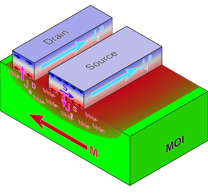
In the following we briefly summarize the physical processes relevant for the experimental configuration shown in Fig. 1. First, a charge current flowing along S is converted into a spin current by the spin Hall effect. has a polarization and is flowing across the interface. Second, this spin current generates a steady state electron spin accumulation in the NM at the MOI/NM interface. Third, by electron-magnon scattering at the MOI/NM interface the spin accumulation is transferred into the MOI, corresponding to the injection of a spin current into the MOI. For the further discussion we have to distinguish between the two cases and . For , the spin current injected into the MOI is rapidly dissipated by spin transfer torque and no long-distance magnon transport is observable. That is, we expect a drain/detector voltage for . In contrast, for spin transfer torque is negligible. In this case a magnon accumulation or depletion is generated at the MOI/NM interface for antiparallel and parallel to , respectively. In the fourth step, this accumulation/depletion will diffusively or ballistically propagate to the drain/detector strip, with details of this transport process depending on temperature, magnon density and scattering rates. Fifth, the magnon propagation will generate a magnon accumulation/depletion at the MOI/NM interface of drain strip D. Finally, inversely to the source strip S, by electron-magnon scattering this accumulation/depletion will be transferred into the electron spin system at the MOI/NM interface. This leads to a spin current in NM which is then converted into a charge current via the ISHE and measured as a voltage in open circuit conditions. Since an electrical current in S causes a voltage drop in the spatially separated D, the phenomenon has been called nonlocal magnetoresistance or, as it is mediated by magnons, magnon mediated magnetoresistance (MMR) [9, 10].
The experimental configuration shown in Fig. 1 has been successfully used to study diffusive magnon transport in YIG thin films grown by liquid phase epitaxy (LPE) and to determine the magnon diffusion length . In the first experimental work by Cornelissen et al. [9] an astonishingly large was found in LPE-YIG at room temperature. This value is very promising for device applications, since the maximum SD separation is limited by . However, values varying by more than two orders of magnitude have been found in subsequent experiments including sputtered YIG and nickel ferrite films (cf. Table 1), indicating that the measured numbers strongly depend on materials properties and details of the device design including the thickness of the MOI [68], fabrication process and data analysis. When comparing and interpreting the measured magnon diffusion lengths, one has to keep in mind that several magnon branches and magnons with different wave number are contributing [76]. This is related to the fact that the magnons are generated by electron-magnon scattering at the MOI/NM interface, resulting in a broad excitation spectrum [73, 74, 41, 66]. Hence, the measured represents an average value obtained for specific experimental conditions. In contrast, experiments using inductive excitation mechanisms can selectively excite certain magnon wavelengths yielding rather different propagation lengths as to the non-local experiments (See Table 1). Another indirect measurement method may be provided by the thermal effects associated to the magnetic excitation transport [77, 78], but requires further experimental studies. Reducing the temperature to was found to result in a vanishingly small detector voltage. This has been interpreted as evidence for a thermally activated nature of the magnon generation process at the MOI/NM interface [66]. Meanwhile, the initial experiments have been confirmed by other groups and led to a deeper understanding of the underlying physics [9, 64, 65, 66, 67, 68, 10, 69, 70, 71, 72]. Interestingly, amorphous YIG thin films also exhibit long-distance magnon-transport in non-local experiments, which may allow to even use disordered spin systems as materials for magnon devices [79].
| material | method | Ref. | ||
|---|---|---|---|---|
| LPE-YIG | optical | [80] | ||
| YIG, sput. | optical | [81] | ||
| YIG, PLD | optical | [82] | ||
| LPE-YIG | inductive | [83] | ||
| LPE-YIG | lateral | [9] | ||
| LPE-YIG | lateral | [10] | ||
| YIG, sput. | 38 | to | vertical | [84] |
| NiFe2O4, sput. | lateral | [67] |
A further crucial parameter is the so-called spin convertance describing the efficiency of the spin transfer between the electron and magnon system at the MOI/NM interface [73, 74]. Very recently, means to enhance the spin convertance have been proposed [71]. In summary, one can say that the measured magnon diffusion lengths in MOIs are promising, but more systematic experiments are required to gain a full quantitative understanding.
(5) Tools for the control and manipulation of spin currents:
Three-terminal, transistor-like devices are highly important for applications. Therefore, regarding the implementation of device concepts not only the generation and detection of spin currents but also the control and manipulation of spin current flow by suitable gate electrodes is required. Research in this direction is only rudimentary and requires more attention. Current approaches are mostly centered on employing reconfigurable magnonic crystals [15, 16]. Another pathway towards spin current control in MOIs is to employ nonlinear magnon-magnon interactions, which can be used for example to suppress a single wavevector magnon current [85]. However, this approach requires large local magnon densities, which may be achieved by making use of the magnon dispersion in magnonic crystals. Ideally, similar to charge based transistor concepts an electrical field control magnon conduction channel would allow for very efficient magnon logic devices.
2.2 Novel Magnetoresistive Effects
The interplay between the electron spin accumulation generated in a NM with strong spin-orbit interaction via the SHE and the non-equilibrium magnon distribution in a MOI at an MOI/NM interface led to novel magnetoresitance phenomena, namely the spin Hall magnetoresistance (SMR) and the magnon mediated magnetoresistance (MMR), which we discuss in more detail in the following.
Spin Hall Magnetoresistance (SMR):
The combination of SHE and ISHE for pure spin current generation and detection in MOI /NM heterostructures led to the discovery of the spin Hall magnetoresistance (SMR) [11, 12, 86, 13]. The SMR is characterized by the dependence of the NM resistance on the angle between charge current direction in the NM and the (sublattice) magnetization orientation in the MOI. In the simplest case of a collinear ferromagnet, an additional contribution to the resistance in the NM arises if the spin polarization of the spin current generated in the NM via the SHE and transferred across the MOI/NM interface is perpendicular to the magnetization in the MOI. For , the dissipation channel resulting from spin transfer torque and, hence, the additional NM resistance is absent. The magnitude of the SMR effect scales with the square of the spin Hall angle of the NM layer, i.e. the interconversion factor between charge and spin current. Experimental values for the relative resistance change of up to have been reported [32, 42]. Most importantly, from these values, which can be obtained from simple magnetotransport measurements, relevant spin transport parameters can be inferred. Furthermore, SMR proved to be a powerful tool also for the investigation of non-collinear magnetic phases (e.g. helical, spin-canting and spin-flip ordering) in MOIs [87, 88]. Especially MOIs with antiferromagnetic order have been investigated using the SMR [89, 90, 91, 92, 93, 94], which further provides evidence that the SMR is sensitive to the magnetic order parameter itself (or possibly the magnetic sublattice moment orientations), but not the net magnetic moment direction. Taken things even a step further, spin currents in NM have meanwhile been used to switch the magnetization of a MOI by the spin transfer torque [95].
Magnon Mediated Magnetoresistance (MMR):
As discussed above, in a device structure as shown in Fig. 1 an electrical current in the source S causes a non-local voltage drop in the spatially separated drain D. Since this phenomenon is based on magnon diffusion between S and D, it is called magnon mediated magnetoresistance (MMR). While the theoretical prediction of MMR was pioneered by Zhang and Zhang [73, 74] in 2012, the first experimental observation was reported in 2015 et al. [9, 10]. Although a detailed knowledge of MMR has not yet been achieved, it is evident already today that MMR has a broad potential for magnon based spintronic devices. Due to a long magnon diffusion length in MOIs lateral device schemes as illustrated in Fig. 1 are feasible with low demands on lateral dimensions. Making use of MMR, electrically controlled magnon logic circuits [69] have already been demonstrated and, very recently, evidence for the magnon transport analogue of the anisotropic magneto resistance in MOIs has been reported [68].
3 Perspectives for Magnetic Insulator based Spintronics
Even today, a rich variety of physical phenomena has been studied in MOIs and successfully used for spintronics applications. Among them are the SMR and MMR, which are powerful tools for probing spin transport across MOI/NM interfaces and magnon propagation in MOIs. MMR already has been successfully used to implement charge-to-spin current converters and magnon-based logic devices [69]. In the following we address some important tasks and key challenges for future research in MOI based spintronics.
Magnon-Based Transistors:
An important task will be the realization of transistor-like structures relying on magnon flow in a MOI controlled by a gate electrode. Here, the key challenge is to develop suitable gate concepts. Controlling magnon flow by an electric gate voltage would be particularly desirable in the context of electronic-magnonic hybrid circuits. Here, multiferroic materials with long magnon diffusion lengths are an option. Research in this direction is expected to also stimulate the realization of novel magnon logic devices.
Selective Magnon Excitation:
Presently, there is little control on magnon excitation in devices relying on the SHE in MOI/NM heterostructures. The development of concepts allowing to selectively excite magnons of specific energy and wave number are a prerequisite for coherent magnon logic circuits using a DC excitation schemes. Possible solutions for selective magnon excitation could be based on magnonic crystals, i.e. on appropriately engineering the magnonic band structure of the MOI [16].
Nonlinear Phenomena:
Another important research task will be the study of nonlinear effects in MOI based devices. A particularly interesting example is the nonlinear dependence of the magnon population in an MOI on the charge current flowing in a NM in devices based on MOI/NM heterostructures. First experiments show that the excitation of magnons with low damping is possible after overcoming a threshold value [96]. Similarly, the generation of magnonic superfluids using spin currents generated via the SHE are already has been proposed [97]. While Bose-Einstein condensation in MOIs has already been experimentally realized using parametric microwave pumping [98, 60], an experimental realization of a magnonic BEC by all-electrical driving has not yet been reported. We note that a magnonic superfluid would coexist with normal magnonic excitations, leading to short-circuiting effects of the magnon transport in MOIs. This allows for novel control schemes for magnonic transport.
Antiferromagnetic Magnonics:
Current experimental studies mostly focus on magnon transport in ferro- or ferrimagnetically ordered MOIs, where typical magnon frequencies are of the order of a few GHz. However, these studies and already developed device concepts can be straightforwardly transferred to antiferromagnetically ordered MOIs as already demonstrated for the spin Seebeck effect [51, 52, 53, 54] and for the spin Hall magnetoresistance [89, 90, 91, 92, 93, 94], thereby extending magnon frequencies to the THz regime [45, 46, 47]. It is expected that this leads to promising applications with an extended frequency regime. A promising example for future applications is the recent demonstration of an antiferromagnetic memory based on the manipulation by the magnetoelectric effect in Cr2O3 thin films and readout via the anomalous Hall effect in a Pt electrode [99]. Clearly, further studies to better understand retainability, stability, repeatability and switching speed are required for successful implementation into new device concepts.
Ballistic Magnon Transport:
Until today, magnon based devices mostly rely on diffusive magnon transport. An important future task will be the detailed study of ballistic magnon transport. A particulary interesting aspect is the study of ballistic magnon transport in one-dimensional transport channels and the demonstration of the quantized magnon conductance in such structures. The experimental challenge is to fabricate one-dimensional magnon transport channels and to reduce the length of these channels below the magnon mean free path. To this end, a possible strategy is to use domain walls in MOIs. We note that the realization of ballistic magnon transport also is promising regarding novel device concepts.
Taken together, within the last decade the successful research on spin current transport in MOIs has lead to a manifold of novel phenomena. This allowed us to get a deeper insight into the fundamental physics and paved the way towards promising applications. Over the next years, further exciting results on fundamental physics aspects and rapid progress regarding transfer into applications are expected.
References
-
[1]
Y. Tserkovnyak, A. Brataas, G. E. W. Bauer,
Spin pumping and
magnetization dynamics in metallic multilayers, Physical Review B 66 (22)
(2002) 224403.
doi:10.1103/physrevb.66.224403.
URL https://doi.org/10.1103/physrevb.66.224403 -
[2]
Y. Tserkovnyak, A. Brataas, G. E. W. Bauer, B. I. Halperin,
Nonlocal magnetization
dynamics in ferromagnetic heterostructures, Reviews of Modern Physics 77 (4)
(2005) 1375–1421.
doi:10.1103/revmodphys.77.1375.
URL https://doi.org/10.1103/revmodphys.77.1375 -
[3]
O. Mosendz, J. E. Pearson, F. Y. Fradin, G. E. W. Bauer, S. D. Bader,
A. Hoffmann,
Quantifying spin Hall
angles from spin pumping: Experiments and theory, Physical Review Letters
104 (4) (2010) 046601.
doi:10.1103/physrevlett.104.046601.
URL https://doi.org/10.1103/physrevlett.104.046601 -
[4]
K. Ando, Y. Kajiwara, K. Sasage, K. Uchida, E. Saitoh,
Inverse spin-Hall effect
induced by spin pumping in various metals, IEEE Trans. Magn. 46 (9) (2010)
3694–3696.
URL http://dx.doi.org/10.1109/TMAG.2010.2060382 -
[5]
K. Uchida, S. Takahashi, K. Harii, J. Ieda, W. Koshibae, K. Ando, S. Maekawa,
E. Saitoh, Observation of the
spin Seebeck effect, Nature 455 (7214) (2008) 778–781.
URL http://dx.doi.org/10.1038/nature07321 -
[6]
K. ichi Uchida, H. Adachi, T. Ota, H. Nakayama, S. Maekawa, E. Saitoh,
Observation of longitudinal
spin-Seebeck effect in magnetic insulators, Appl. Phys. Lett. 97 (17)
(2010) 172505.
URL http://dx.doi.org/10.1063/1.3507386 -
[7]
J. Xiao, G. E. W. Bauer, K. chi Uchida, E. Saitoh, S. Maekawa,
Theory of magnon-driven
spin Seebeck effect, Physical Review B 81 (21) (2010) 214418.
doi:10.1103/physrevb.81.214418.
URL https://doi.org/10.1103/physrevb.81.214418 -
[8]
G. E. W. Bauer, E. Saitoh, B. J. van Wees,
Spin caloritronics, Nature Materials
11 (5) (2012) 391–399.
doi:10.1038/nmat3301.
URL https://doi.org/10.1038/nmat3301 -
[9]
L. J. Cornelissen, J. Liu, R. A. Duine, J. B. Youssef, B. J. van Wees,
Long-distance transport of magnon
spin information in a magnetic insulator at room temperature, Nature Physics
11 (12) (2015) 1022–1026.
doi:10.1038/nphys3465.
URL https://doi.org/10.1038/nphys3465 -
[10]
S. T. B. Goennenwein, R. Schlitz, M. Pernpeintner, K. Ganzhorn, M. Althammer,
R. Gross, H. Huebl, Non-local
magnetoresistance in YIG/Pt nanostructures, Applied Physics Letters
107 (17) (2015) 172405.
doi:10.1063/1.4935074.
URL https://doi.org/10.1063/1.4935074 -
[11]
H. Nakayama, M. Althammer, Y.-T. Chen, K. Uchida, Y. Kajiwara, D. Kikuchi,
T. Ohtani, S. Geprägs, M. Opel, S. Takahashi, R. Gross, G. E. W. Bauer,
S. T. B. Goennenwein, E. Saitoh,
Spin Hall
magnetoresistance induced by a nonequilibrium proximity effect, Phys. Rev.
Lett. 110 (20) (2013) 206601.
URL http://link.aps.org/doi/10.1103/PhysRevLett.110.206601 -
[12]
N. Vlietstra, J. Shan, V. Castel, B. J. van Wees, J. B. Youssef,
Spin-Hall
magnetoresistance in platinum on yttrium iron garnet: Dependence on platinum
thickness and in-plane/out-of-plane magnetization, Phys. Rev. B 87 (18).
URL http://dx.doi.org/10.1103/PhysRevB.87.184421 -
[13]
Y.-T. Chen, S. Takahashi, H. Nakayama, M. Althammer, S. T. B. Goennenwein,
E. Saitoh, G. E. W. Bauer,
Theory of spin
Hall magnetoresistance, Phys. Rev. B 87 (14) (2013) 144411.
URL http://link.aps.org/doi/10.1103/PhysRevB.87.144411 -
[14]
A. B. Cahaya, O. A. Tretiakov, G. E. W. Bauer,
Spin Seebeck power
conversion, IEEE Transactions on Magnetics 51 (9) (2015) 1–14.
doi:10.1109/tmag.2015.2436362.
URL https://doi.org/10.1109/tmag.2015.2436362 -
[15]
A. V. Chumak, V. I. Vasyuchka, A. A. Serga, B. Hillebrands,
Magnon spintronics, Nature Physics
11 (6) (2015) 453–461.
doi:10.1038/nphys3347.
URL https://doi.org/10.1038/nphys3347 -
[16]
A. V. Chumak, A. A. Serga, B. Hillebrands,
Magnonic crystals for data
processing, Journal of Physics D: Applied Physics 50 (24) (2017) 244001.
doi:10.1088/1361-6463/aa6a65.
URL https://doi.org/10.1088/1361-6463/aa6a65 -
[17]
B. Heinrich, C. Burrowes, E. Montoya, B. Kardasz, E. Girt, Y.-Y. Song, Y. Sun,
M. Wu, Spin pumping at
the magnetic insulator (YIG)/normal metal (Au) interfaces, Physical
Review Letters 107 (6) (2011) 066604.
doi:10.1103/physrevlett.107.066604.
URL https://doi.org/10.1103/physrevlett.107.066604 -
[18]
F. D. Czeschka, L. Dreher, M. S. Brandt, M. Weiler, M. Althammer, I.-M. Imort,
G. Reiss, A. Thomas, W. Schoch, W. Limmer, H. Huebl, R. Gross, S. T. B.
Goennenwein, Scaling
behavior of the spin pumping effect in ferromagnet-platinum bilayers, Phys.
Rev. Lett. 107 (4).
URL http://dx.doi.org/10.1103/PhysRevLett.107.046601 -
[19]
C. Burrowes, B. Heinrich, B. Kardasz, E. A. Montoya, E. Girt, Y. Sun, Y.-Y.
Song, M. Wu, Enhanced spin pumping
at yttrium iron garnet/Au interfaces, Applied Physics Letters 100 (9)
(2012) 092403.
doi:10.1063/1.3690918.
URL https://doi.org/10.1063/1.3690918 -
[20]
C. Hahn, G. de Loubens, M. Viret, O. Klein, V. V. Naletov, J. B. Youssef,
Detection of microwave
spin pumping using the inverse spin Hall effect, Physical Review Letters
111 (21) (2013) 217204.
doi:10.1103/physrevlett.111.217204.
URL https://doi.org/10.1103/physrevlett.111.217204 -
[21]
H. Jiao, G. E. W. Bauer,
Spin backflow and ac
voltage generation by spin pumping and the inverse spin Hall effect,
Physical Review Letters 110 (21) (2013) 217602.
doi:10.1103/physrevlett.110.217602.
URL https://doi.org/10.1103/physrevlett.110.217602 -
[22]
K. Uchida, H. Adachi, T. An, T. Ota, M. Toda, B. Hillebrands, S. Maekawa,
E. Saitoh, Long-range spin Seebeck
effect and acoustic spin pumping, Nature Materials 10 (10) (2011) 737–741.
doi:10.1038/nmat3099.
URL https://doi.org/10.1038/nmat3099 -
[23]
K. Uchida, H. Adachi, T. An, H. Nakayama, M. Toda, B. Hillebrands, S. Maekawa,
E. Saitoh, Acoustic spin pumping:
Direct generation of spin currents from sound waves in Pt/y3fe5o12hybrid
structures, Journal of Applied Physics 111 (5) (2012) 053903.
doi:10.1063/1.3688332.
URL https://doi.org/10.1063/1.3688332 -
[24]
M. Weiler, H. Huebl, F. S. Goerg, F. D. Czeschka, R. Gross, S. T. B.
Goennenwein, Spin
pumping with coherent elastic waves, Physical Review Letters 108 (17) (2012)
176601.
doi:10.1103/physrevlett.108.176601.
URL https://doi.org/10.1103/physrevlett.108.176601 -
[25]
A. Slachter, F. L. Bakker, J.-P. Adam, B. J. van Wees,
Thermally driven spin injection from
a ferromagnet into a non-magnetic metal, Nature Physics 6 (11) (2010)
879–882.
doi:10.1038/nphys1767.
URL https://doi.org/10.1038/nphys1767 -
[26]
M. Weiler, M. Althammer, F. D. Czeschka, H. Huebl, M. S. Wagner, M. Opel, I.-M.
Imort, G. Reiss, A. Thomas, R. Gross, S. T. B. Goennenwein,
Local charge and spin
currents in magnetothermal landscapes, Phys. Rev. Lett. 108 (10) (2012)
106602.
URL http://dx.doi.org/10.1103/PhysRevLett.108.106602 -
[27]
H. Adachi, K. ichi Uchida, E. Saitoh, S. Maekawa,
Theory of the spin
Seebeck effect, Reports on Progress in Physics 76 (3) (2013) 036501.
doi:10.1088/0034-4885/76/3/036501.
URL https://doi.org/10.1088/0034-4885/76/3/036501 -
[28]
M. Schreier, N. Roschewsky, E. Dobler, S. Meyer, H. Huebl, R. Gross, S. T. B.
Goennenwein, Current heating
induced spin Seebeck effect, Appl. Phys. Lett. 103 (24) (2013) 242404.
doi:10.1063/1.4839395.
URL http://dx.doi.org/10.1063/1.4839395 -
[29]
S. M. Rezende, R. L. Rodríguez-Suárez, R. O. Cunha, A. R.
Rodrigues, F. L. A. Machado, G. A. F. Guerra, J. C. L. Ortiz, A. Azevedo,
Magnon spin-current theory
for the longitudinal spin-Seebeck effect, Physical Review B 89 (1) (2014)
014416.
doi:10.1103/physrevb.89.014416.
URL https://doi.org/10.1103/physrevb.89.014416 -
[30]
K. Uchida, M. Ishida, T. Kikkawa, A. Kirihara, T. Murakami, E. Saitoh,
Longitudinal spin
Seebeck effect: from fundamentals to applications, Journal of Physics:
Condensed Matter 26 (34) (2014) 343202.
doi:10.1088/0953-8984/26/34/343202.
URL https://doi.org/10.1088/0953-8984/26/34/343202 -
[31]
L. Liu, T. Moriyama, D. C. Ralph, R. A. Buhrman,
Spin-torque
ferromagnetic resonance induced by the spin Hall effect, Physical Review
Letters 106 (3) (2011) 036601.
doi:10.1103/physrevlett.106.036601.
URL https://doi.org/10.1103/physrevlett.106.036601 -
[32]
M. Althammer, S. Meyer, H. Nakayama, M. Schreier, S. Altmannshofer, M. Weiler,
H. Huebl, S. Geprägs, M. Opel, R. Gross, D. Meier, C. Klewe, T. Kuschel,
J.-M. Schmalhorst, G. Reiss, L. Shen, A. Gupta, Y.-T. Chen, G. E. W. Bauer,
E. Saitoh, S. T. B. Goennenwein,
Quantitative study
of the spin Hall magnetoresistance in ferromagnetic insulator/normal metal
hybrids, Phys. Rev. B 87 (22) (2013) 224401.
doi:10.1103/PhysRevB.87.224401.
URL http://link.aps.org/doi/10.1103/PhysRevB.87.224401 -
[33]
M. Dyakonov, V. Perel,
Current-induced
spin orientation of electrons in semiconductors, Physics Letters A 35 (6)
(1971) 459–460.
doi:10.1016/0375-9601(71)90196-4.
URL https://doi.org/10.1016%2F0375-9601%2871%2990196-4 -
[34]
J. E. Hirsch, Spin Hall
effect, Physical Review Letters 83 (9) (1999) 1834–1837.
doi:10.1103/physrevlett.83.1834.
URL https://doi.org/10.1103/physrevlett.83.1834 -
[35]
A. Hoffmann, Spin Hall
effects in metals, IEEE Transactions on Magnetics 49 (10) (2013)
5172–5193.
doi:10.1109/tmag.2013.2262947.
URL https://doi.org/10.1109/tmag.2013.2262947 -
[36]
J. Sinova, S. O. Valenzuela, J. Wunderlich, C. Back, T. Jungwirth,
Spin Hall effects,
Reviews of Modern Physics 87 (4) (2015) 1213–1260.
doi:10.1103/revmodphys.87.1213.
URL https://doi.org/10.1103/revmodphys.87.1213 -
[37]
D. Xiao, M.-C. Chang, Q. Niu,
Berry phase
effects on electronic properties, Reviews of Modern Physics 82 (3) (2010)
1959–2007.
doi:10.1103/RevModPhys.82.1959.
URL https://link.aps.org/doi/10.1103/RevModPhys.82.1959 -
[38]
L. Liu, O. J. Lee, T. J. Gudmundsen, D. C. Ralph, R. A. Buhrman,
Current-induced
switching of perpendicularly magnetized magnetic layers using spin torque
from the spin Hall effect, Physical Review Letters 109 (9) (2012) 096602.
doi:10.1103/physrevlett.109.096602.
URL https://doi.org/10.1103/physrevlett.109.096602 -
[39]
C.-F. Pai, L. Liu, Y. Li, H. W. Tseng, D. C. Ralph, R. A. Buhrman,
Spin transfer torque devices
utilizing the giant spin Hall effect of tungsten, Applied Physics Letters
101 (12) (2012) 122404.
doi:10.1063/1.4753947.
URL https://doi.org/10.1063/1.4753947 -
[40]
L. Liu, C.-F. Pai, Y. Li, H. W. Tseng, D. C. Ralph, R. A. Buhrman,
Spin-torque switching with the
giant spin Hall effect of tantalum, Science 336 (6081) (2012) 555–558.
doi:10.1126/science.1218197.
URL https://doi.org/10.1126/science.1218197 -
[41]
S. A. Bender, Y. Tserkovnyak,
Interfacial spin and heat
transfer between metals and magnetic insulators, Physical Review B 91 (14)
(2015) 140402.
doi:10.1103/physrevb.91.140402.
URL https://doi.org/10.1103/physrevb.91.140402 -
[42]
M. Weiler, M. Althammer, M. Schreier, J. Lotze, M. Pernpeintner, S. Meyer,
H. Huebl, R. Gross, A. Kamra, J. Xiao, Y.-T. Chen, H. Jiao, G. E. W. Bauer,
S. T. B. Goennenwein,
Experimental
test of the spin mixing interface conductivity concept, Phys. Rev. Lett.
111 (17) (2013) 176601.
URL http://link.aps.org/doi/10.1103/PhysRevLett.111.176601 -
[43]
T. Kampfrath, M. Battiato, P. Maldonado, G. Eilers, J. Nötzold,
S. Mährlein, V. Zbarsky, F. Freimuth, Y. Mokrousov, S. Blügel,
M. Wolf, I. Radu, P. M. Oppeneer, M. Münzenberg,
Terahertz spin current pulses
controlled by magnetic heterostructures, Nature Nanotechnology 8 (4) (2013)
256–260.
doi:10.1038/nnano.2013.43.
URL https://doi.org/10.1038/nnano.2013.43 -
[44]
M. Weiler, J. M. Shaw, H. T. Nembach, T. J. Silva,
Phase-sensitive
detection of spin pumping via the ac inverse spin Hall effect, Physical
Review Letters 113 (15) (2014) 157204.
doi:10.1103/physrevlett.113.157204.
URL https://doi.org/10.1103/physrevlett.113.157204 -
[45]
R. Cheng, J. Xiao, Q. Niu, A. Brataas,
Spin pumping and
spin-transfer torques in antiferromagnets, Physical Review Letters 113 (5)
(2014) 057601.
doi:10.1103/physrevlett.113.057601.
URL https://doi.org/10.1103/physrevlett.113.057601 -
[46]
R. Cheng, D. Xiao, A. Brataas,
Terahertz
antiferromagnetic spin Hall nano-oscillator, Physical Review Letters
116 (20) (2016) 207603.
doi:10.1103/physrevlett.116.207603.
URL https://doi.org/10.1103/Fphysrevlett.116.207603 -
[47]
Ø. Johansen, A. Brataas,
Spin pumping and inverse
spin Hall voltages from dynamical antiferromagnets, Physical Review B
95 (22) (2017) 220408.
doi:10.1103/physrevb.95.220408.
URL https://doi.org/10.1103/physrevb.95.220408 -
[48]
B. L. Giles, Z. Yang, J. S. Jamison, R. C. Myers,
Long-range pure magnon spin
diffusion observed in a nonlocal spin-Seebeck geometry, Physical Review B
92 (22).
doi:10.1103/physrevb.92.224415.
URL https://doi.org/10.1103/physrevb.92.224415 -
[49]
S. Geprägs, A. Kehlberger, F. D. Coletta, Z. Qiu, E.-J. Guo, T. Schulz,
C. Mix, S. Meyer, A. Kamra, M. Althammer, H. Huebl, G. Jakob, Y. Ohnuma,
H. Adachi, J. Barker, S. Maekawa, G. E. W. Bauer, E. Saitoh, R. Gross,
S. T. B. Goennenwein, M. Kläui,
Origin of the spin Seebeck
effect in compensated ferrimagnets, Nature Communications 7 (2016) 10452.
doi:10.1038/ncomms10452.
URL https://doi.org/10.1038/ncomms10452 -
[50]
A. Kirihara, K. ichi Uchida, Y. Kajiwara, M. Ishida, Y. Nakamura, T. Manako,
E. Saitoh, S. Yorozu,
Spin-current-driven thermoelectric
coating, Nature Materials 11 (8) (2012) 686–689.
doi:10.1038/nmat3360.
URL https://doi.org/10.1038/nmat3360 -
[51]
S. Seki, T. Ideue, M. Kubota, Y. Kozuka, R. Takagi, M. Nakamura, Y. Kaneko,
M. Kawasaki, Y. Tokura,
Thermal
generation of spin current in an antiferromagnet, Physical Review Letters
115 (26) (2015) 266601.
doi:10.1103/PhysRevLett.115.266601.
URL https://link.aps.org/doi/10.1103/PhysRevLett.115.266601 -
[52]
S. M. Wu, W. Zhang, A. Kc, P. Borisov, J. E. Pearson, J. S. Jiang, D. Lederman,
A. Hoffmann, A. Bhattacharya,
Antiferromagnetic
spin Seebeck effect, Physical Review Letters 116 (9) (2016) 097204.
doi:10.1103/PhysRevLett.116.097204.
URL https://link.aps.org/doi/10.1103/PhysRevLett.116.097204 -
[53]
S. M. Rezende, R. L. Rodríguez-Suárez, A. Azevedo,
Theory of the spin
Seebeck effect in antiferromagnets, Physical Review B 93 (1) (2016)
014425.
doi:10.1103/PhysRevB.93.014425.
URL https://link.aps.org/doi/10.1103/PhysRevB.93.014425 -
[54]
J. Holanda, D. S. Maior, O. Alves Santos, L. H. Vilela-Leão, J. B. S. Mendes,
A. Azevedo, R. L. Rodríguez-Suárez, S. M. Rezende,
Spin Seebeck effect
in the antiferromagnet nickel oxide at room temperature, Applied Physics
Letters 111 (17) (2017) 172405.
doi:10.1063/1.5001694.
URL http://aip.scitation.org/doi/10.1063/1.5001694 -
[55]
X. Wang, C. O. Pauyac, A. Manchon,
Spin-orbit-coupled
transport and spin torque in a ferromagnetic heterostructure, Physical
Review B 89 (5).
doi:10.1103/physrevb.89.054405.
URL https://doi.org/10.1103/physrevb.89.054405 -
[56]
M. Jamali, J. S. Lee, J. S. Jeong, F. Mahfouzi, Y. Lv, Z. Zhao, B. K.
Nikolić, K. A. Mkhoyan, N. Samarth, J.-P. Wang,
Giant spin pumping and
inverse spin Hall effect in the presence of surface and bulk spin-orbit
coupling of topological insulator Bi2Se3, Nano Letters 15 (10) (2015)
7126–7132.
doi:10.1021/acs.nanolett.5b03274.
URL https://doi.org/10.1021/acs.nanolett.5b03274 - [57] M. Sparks, Ferromagnetic-Relaxation Theory, McGraw-Hill, 1964.
- [58] A. G. Gurevich, G. A. Melkov, Magnetization Oscillations and Waves, CRC Press, 1996.
-
[59]
S. Demokritov, Brillouin
light scattering studies of confined spin waves: linear and nonlinear
confinement, Physics Reports 348 (6) (2001) 441–489.
doi:10.1016/s0370-1573(00)00116-2.
URL https://doi.org/10.1016/s0370-1573(00)00116-2 -
[60]
V. E. Demidov, O. Dzyapko, S. O. Demokritov, G. A. Melkov, A. N. Slavin,
Thermalization of a
parametrically driven magnon gas leading to bose-einstein condensation,
Physical Review Letters 99 (3) (2007) 037205.
doi:10.1103/physrevlett.99.037205.
URL https://doi.org/10.1103/physrevlett.99.037205 -
[61]
V. E. Demidov, O. Dzyapko, M. Buchmeier, T. Stockhoff, G. Schmitz, G. A.
Melkov, S. O. Demokritov,
Magnon kinetics and
bose-einstein condensation studied in phase space, Physical Review Letters
101 (25) (2008) 257201.
doi:10.1103/physrevlett.101.257201.
URL https://doi.org/10.1103/physrevlett.101.257201 -
[62]
S. Demokritov, V. Demidov,
Micro-brillouin light
scattering spectroscopy of magnetic nanostructures, IEEE Transactions on
Magnetics 44 (1) (2008) 6–12.
doi:10.1109/tmag.2007.910227.
URL https://doi.org/10.1109/tmag.2007.910227 -
[63]
T. Sebastian, K. Schultheiss, B. Obry, B. Hillebrands, H. Schultheiss,
Micro-focused brillouin light
scattering: imaging spin waves at the nanoscale, Frontiers in Physics 3.
doi:10.3389/fphy.2015.00035.
URL https://doi.org/10.3389/fphy.2015.00035 -
[64]
L. J. Cornelissen, K. J. H. Peters, G. E. W. Bauer, R. A. Duine, B. J. van
Wees, Magnon spin transport
driven by the magnon chemical potential in a magnetic insulator, Physical
Review B 94 (1) (2016) 014412.
doi:10.1103/physrevb.94.014412.
URL https://doi.org/10.1103/physrevb.94.014412 -
[65]
L. J. Cornelissen, B. J. van Wees,
Magnetic field dependence
of the magnon spin diffusion length in the magnetic insulator yttrium iron
garnet, Physical Review B 93 (2) (2016) 020403.
doi:10.1103/physrevb.93.020403.
URL https://doi.org/10.1103/physrevb.93.020403 -
[66]
L. J. Cornelissen, J. Shan, B. J. van Wees,
Temperature dependence of
the magnon spin diffusion length and magnon spin conductivity in the magnetic
insulator yttrium iron garnet, Physical Review B 94 (18) (2016) 180402.
doi:10.1103/physrevb.94.180402.
URL https://doi.org/10.1103/physrevb.94.180402 -
[67]
J. Shan, P. Bougiatioti, L. Liang, G. Reiss, T. Kuschel, B. J. van Wees,
Nonlocal magnon spin transport in
NiFe2o4 thin films, Applied Physics Letters 110 (13) (2017) 132406.
doi:10.1063/1.4979408.
URL https://doi.org/10.1063/1.4979408 -
[68]
J. Liu, L. J. Cornelissen, J. Shan, T. Kuschel, B. J. van Wees,
Magnon planar Hall effect
and anisotropic magnetoresistance in a magnetic insulator, Physical Review B
95 (14).
doi:10.1103/physrevb.95.140402.
URL https://doi.org/10.1103/physrevb.95.140402 -
[69]
K. Ganzhorn, S. Klingler, T. Wimmer, S. Geprägs, R. Gross, H. Huebl,
S. T. B. Goennenwein, Magnon-based
logic in a multi-terminal YIG/Pt nanostructure, Applied Physics Letters
109 (2) (2016) 022405.
doi:10.1063/1.4958893.
URL https://doi.org/10.1063/1.4958893 -
[70]
K. Ganzhorn, T. Wimmer, J. Cramer, R. Schlitz, S. Geprägs, G. Jakob,
R. Gross, H. Huebl, M. Kläui, S. T. B. Goennenwein,
Temperature dependence of the
non-local spin Seebeck effect in YIG/Pt nanostructures, AIP Advances
7 (8) (2017) 085102.
doi:10.1063/1.4986848.
URL https://doi.org/10.1063/1.4986848 -
[71]
S. Vélez, A. Bedoya-Pinto, W. Yan, L. E. Hueso, F. Casanova,
Competing effects at
Pt/YIG interfaces: Spin Hall magnetoresistance, magnon excitations, and
magnetic frustration, Physical Review B 94 (17).
doi:10.1103/physrevb.94.174405.
URL https://doi.org/10.1103/physrevb.94.174405 -
[72]
J. Li, Y. Xu, M. Aldosary, C. Tang, Z. Lin, S. Zhang, R. Lake, J. Shi,
Observation of magnon-mediated
current drag in Pt/yttrium iron garnet/Pt(Ta) trilayers, Nature
Communications 7 (2016) 10858.
doi:10.1038/ncomms10858.
URL https://doi.org/10.1038/ncomms10858 -
[73]
S. S.-L. Zhang, S. Zhang,
Magnon mediated
electric current drag across a ferromagnetic insulator layer, Physical
Review Letters 109 (9) (2012) 096603.
doi:10.1103/physrevlett.109.096603.
URL https://doi.org/10.1103/physrevlett.109.096603 -
[74]
S. S.-L. Zhang, S. Zhang,
Spin convertance at
magnetic interfaces, Physical Review B 86 (21) (2012) 214424.
doi:10.1103/physrevb.86.214424.
URL https://doi.org/10.1103/physrevb.86.214424 -
[75]
Y. Cheng, K. Chen, S. Zhang,
Interplay of magnon and
electron currents in magnetic heterostructure, Physical Review B 96 (2)
(2017) 024449.
doi:10.1103/physrevb.96.024449.
URL https://doi.org/10.1103/physrevb.96.024449 -
[76]
V. Cherepanov, I. Kolokolov, V. L’vov,
The saga of YIG:
Spectra, thermodynamics, interaction and relaxation of magnons in a complex
magnet, Physics Reports 229 (3) (1993) 81–144.
doi:10.1016/0370-1573(93)90107-o.
URL https://doi.org/10.1016/0370-1573(93)90107-o -
[77]
Y. Onose, T. Ideue, H. Katsura, Y. Shiomi, N. Nagaosa, Y. Tokura,
Observation
of the Magnon Hall Effect, Science 329 (5989) (2010) 297–299.
doi:10.1126/science.1188260.
URL http://www.sciencemag.org/cgi/doi/10.1126/science.1188260 -
[78]
T. An, V. I. Vasyuchka, K. Uchida, A. V. Chumak, K. Yamaguchi, K. Harii,
J. Ohe, M. B. Jungfleisch, Y. Kajiwara, H. Adachi, B. Hillebrands,
S. Maekawa, E. Saitoh,
Unidirectional
spin-wave heat conveyer, Nature Materials 12 (6) (2013) 549–553.
doi:10.1038/nmat3628.
URL http://www.nature.com/doifinder/10.1038/nmat3628 -
[79]
D. Wesenberg, T. Liu, D. Balzar, M. Wu, B. L. Zink,
Long-distance spin
transport in a disordered magnetic insulator, Nature Physics 13 (10) (2017)
987–993.
doi:10.1038/nphys4175.
URL http://www.nature.com/doifinder/10.1038/nphys4175 -
[80]
P. Pirro, T. Brächer, A. V. Chumak, B. Lägel, C. Dubs, O. Surzhenko,
P. Görnert, B. Leven, B. Hillebrands,
Spin-wave excitation
and propagation in microstructured waveguides of yttrium iron garnet/Pt
bilayers, Applied Physics Letters 104 (1) (2014) 012402.
doi:10.1063/1.4861343.
URL http://aip.scitation.org/doi/10.1063/1.4861343 -
[81]
M. B. Jungfleisch, W. Zhang, W. Jiang, H. Chang, J. Sklenar, S. M. Wu, J. E.
Pearson, A. Bhattacharya, J. B. Ketterson, M. Wu, A. Hoffmann,
Spin waves in
micro-structured yttrium iron garnet nanometer-thick films, Journal of
Applied Physics 117 (17) (2015) 17D128.
doi:10.1063/1.4916027.
URL http://aip.scitation.org/doi/10.1063/1.4916027 -
[82]
M. Collet, O. Gladii, M. Evelt, V. Bessonov, L. Soumah, P. Bortolotti, S. O.
Demokritov, Y. Henry, V. Cros, M. Bailleul, V. E. Demidov, A. Anane,
Spin-wave propagation
in ultra-thin YIG based waveguides, Applied Physics Letters 110 (9) (2017)
092408.
doi:10.1063/1.4976708.
URL http://aip.scitation.org/doi/10.1063/1.4976708 -
[83]
S. Maendl, I. Stasinopoulos, D. Grundler,
Spin waves with large
decay length and few 100 nm wavelengths in thin yttrium iron garnet grown at
the wafer scale, Applied Physics Letters 111 (1) (2017) 012403.
doi:10.1063/1.4991520.
URL http://aip.scitation.org/doi/10.1063/1.4991520 -
[84]
H. Wu, C. H. Wan, X. Zhang, Z. H. Yuan, Q. T. Zhang, J. Y. Qin, H. X. Wei,
X. F. Han, S. Zhang,
Observation of
magnon-mediated electric current drag at room temperature, Physical Review B
93 (6) (2016) 060403.
doi:10.1103/physrevb.93.060403.
URL https://doi.org/10.1103/physrevb.93.060403 -
[85]
A. V. Chumak, A. A. Serga, B. Hillebrands,
Magnon transistor
for all-magnon data processing, Nature Communications 5 (2014) 4700.
doi:10.1038/ncomms5700.
URL http://www.nature.com/doifinder/10.1038/ncomms5700 -
[86]
C. Hahn, G. de Loubens, O. Klein, M. Viret, V. V. Naletov, J. B. Youssef,
Comparative measurements
of inverse spin Hall effects and magnetoresistance in YIG/Pt and
YIG/Ta, Phys. Rev. B 87 (17) (2013) 174417.
URL http://dx.doi.org/10.1103/PhysRevB.87.174417 -
[87]
A. Aqeel, N. Vlietstra, J. A. Heuver, G. E. W. Bauer, B. Noheda, B. J. van
Wees, T. T. M. Palstra,
Spin-Hall
magnetoresistance and spin Seebeck effect in spin-spiral and paramagnetic
phases of multiferroic CoCr 2 o 4 films, Phys. Rev. B 92 (22) (2015)
224410.
URL http://dx.doi.org/10.1103/PhysRevB.92.224410 -
[88]
K. Ganzhorn, J. Barker, R. Schlitz, B. A. Piot, K. Ollefs, F. Guillou,
F. Wilhelm, A. Rogalev, M. Opel, M. Althammer, S. Geprägs, H. Huebl,
R. Gross, G. E. W. Bauer, S. T. B. Goennenwein,
Spin Hall
magnetoresistance in a canted ferrimagnet, Physical Review B 94 (9) (2016)
094401.
doi:10.1103/physrevb.94.094401.
URL https://doi.org/10.1103/physrevb.94.094401 -
[89]
J. H. Han, C. Song, F. Li, Y. Y. Wang, G. Y. Wang, Q. H. Yang, F. Pan,
Antiferromagnet-controlled
spin current transport in SrMnO 3 / Pt hybrids, Physical Review B
90 (14) (2014) 144431.
doi:10.1103/PhysRevB.90.144431.
URL https://link.aps.org/doi/10.1103/PhysRevB.90.144431 -
[90]
A. Manchon, Spin Hall
magnetoresistance in antiferromagnet/normal metal bilayers, physica status
solidi (RRL) - Rapid Research Letters 11 (4) (2017) 1600409.
doi:10.1002/pssr.201600409.
URL http://doi.wiley.com/10.1002/pssr.201600409 -
[91]
D. Hou, Z. Qiu, J. Barker, K. Sato, K. Yamamoto, S. Vélez, J. M. Gomez-Perez,
L. E. Hueso, F. Casanova, E. Saitoh,
Tunable Sign
Change of Spin Hall Magnetoresistance in Pt / NiO / YIG
Structures, Physical Review Letters 118 (14) (2017) 147202.
doi:10.1103/PhysRevLett.118.147202.
URL http://link.aps.org/doi/10.1103/PhysRevLett.118.147202 -
[92]
Y. Ji, J. Miao, K. K. Meng, Z. Y. Ren, B. W. Dong, X. G. Xu, Y. Wu, Y. Jiang,
Spin Hall
magnetoresistance in an antiferromagnetic magnetoelectric Cr
O /heavy-metal W heterostructure,
Applied Physics Letters 110 (26) (2017) 262401.
doi:10.1063/1.4989680.
URL http://aip.scitation.org/doi/10.1063/1.4989680 -
[93]
G. R. Hoogeboom, A. Aqeel, T. Kuschel, T. T. M. Palstra, B. J. van Wees,
Negative spin Hall
magnetoresistance of Pt on the bulk easy-plane antiferromagnet NiO,
Applied Physics Letters 111 (5) (2017) 052409.
doi:10.1063/1.4997588.
URL http://aip.scitation.org/doi/10.1063/1.4997588 -
[94]
J. Fischer, O. Gomonay, R. Schlitz, K. Ganzhorn, N. Vlietstra, M. Althammer,
H. Huebl, M. Opel, R. Gross, S. T. B. Goennenwein, S. Geprägs,
Spin Hall magnetoresistance in
antiferromagnet/normal metal heterostructures, arXiv:1709.04158
[cond-mat]ArXiv: 1709.04158.
URL http://arxiv.org/abs/1709.04158 -
[95]
C. O. Avci, A. Quindeau, C.-F. Pai, M. Mann, L. Caretta, A. S. Tang, M. C.
Onbasli, C. A. Ross, G. S. D. Beach,
Current-induced switching in a
magnetic insulator, Nature Materials 16 (3) (2016) 309–314.
doi:10.1038/nmat4812.
URL https://doi.org/10.1038/nmat4812 - [96] N. Thiery, A. Draveny, V. V. Naletov, L. Vila, J.-P. Attané, G. de Loubens, M. Viret, N. Beaulieu, J. Ben Youssef, V. E. Demidov, S. O. Demokritov, A. N. Slain, V. S. Tiberkevich, A. Anane, P. Bortolotti, V. Cros, O. Klein, Spin conductance of YIG thin films driven from thermal to subthermal magnons regime by large spin-orbit torque, ArXiv e-printsarXiv:1702.05226.
-
[97]
S. Takei, Y. Tserkovnyak,
Nonlocal
magnetoresistance mediated by spin superfluidity, Physical Review Letters
115 (15).
doi:10.1103/physrevlett.115.156604.
URL https://doi.org/10.1103/physrevlett.115.156604 -
[98]
S. O. Demokritov, V. E. Demidov, O. Dzyapko, G. A. Melkov, A. A. Serga,
B. Hillebrands, A. N. Slavin,
Bose–einstein
condensation of quasi-equilibrium magnons at room temperature under pumping,
Nature 443 (7110) (2006) 430–433.
doi:10.1038/nature05117.
URL https://doi.org/10.1038/nature05117 -
[99]
T. Kosub, M. Kopte, R. Hühne, P. Appel, B. Shields, P. Maletinsky, R. Hübner,
M. O. Liedke, J. Fassbender, O. G. Schmidt, D. Makarov,
Purely
antiferromagnetic magnetoelectric random access memory, Nature
Communications 8 (2017) 13985.
doi:10.1038/ncomms13985.
URL http://www.nature.com/doifinder/10.1038/ncomms13985