Understanding and Improving
the Latency of DRAM-Based Memory
Systems
Abstract
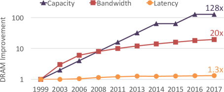
Over the past two decades, the storage capacity and access bandwidth of main memory have improved tremendously, by 128x and 20x, respectively. These improvements are mainly due to the continuous technology scaling of DRAM (dynamic random-access memory), which has been used as the physical substrate for main memory. In stark contrast with capacity and bandwidth, DRAM latency has remained almost constant, reducing by only 1.3x in the same time frame. Therefore, long DRAM latency continues to be a critical performance bottleneck in modern systems. Increasing core counts, and the emergence of increasingly more data-intensive and latency-critical applications further stress the importance of providing low-latency memory access.
In this dissertation, we identify three main problems that contribute significantly to long latency of DRAM accesses. To address these problems, we present a series of new techniques. Our new techniques significantly improve both system performance and energy efficiency. We also examine the critical relationship between supply voltage and latency in modern DRAM chips and develop new mechanisms that exploit this voltage-latency trade-off to improve energy efficiency.
First, while bulk data movement is a key operation in many applications and operating systems, contemporary systems perform this movement inefficiently, by transferring data from DRAM to the processor, and then back to DRAM, across a narrow off-chip channel. The use of this narrow channel for bulk data movement results in high latency and high energy consumption. This dissertation introduces a new DRAM design, Low-cost Inter-linked SubArrays (LISA), which provides fast and energy-efficient bulk data movement across subarrays in a DRAM chip. We show that the LISA substrate is very powerful and versatile by demonstrating that it efficiently enables several new architectural mechanisms, including low-latency data copying, reduced DRAM access latency for frequently-accessed data, and reduced preparation latency for subsequent accesses to a DRAM bank.
Second, DRAM needs to be periodically refreshed to prevent data loss due to leakage. Unfortunately, while DRAM is being refreshed, a part of it becomes unavailable to serve memory requests, which degrades system performance. To address this refresh interference problem, we propose two access-refresh parallelization techniques that enable more overlapping of accesses with refreshes inside DRAM, at the cost of very modest changes to the memory controllers and DRAM chips. These two techniques together achieve performance close to an idealized system that does not require refresh.
Third, we find, for the first time, that there is significant latency variation in accessing different cells of a single DRAM chip due to the irregularity in the DRAM manufacturing process. As a result, some DRAM cells are inherently faster to access, while others are inherently slower. Unfortunately, existing systems do not exploit this variation and use a fixed latency value based on the slowest cell across all DRAM chips. To exploit latency variation within the DRAM chip, we experimentally characterize and understand the behavior of the variation that exists in real commodity DRAM chips. Based on our characterization, we propose Flexible-LatencY DRAM (FLY-DRAM), a mechanism to reduce DRAM latency by categorizing the DRAM cells into fast and slow regions, and accessing the fast regions with a reduced latency, thereby improving system performance significantly. Our extensive experimental characterization and analysis of latency variation in DRAM chips can also enable the development of other new techniques to improve performance or reliability.
Fourth, this dissertation, for the first time, develops an understanding of the latency behavior due to another important factor – supply voltage, which significantly impacts DRAM performance, energy consumption, and reliability. We take an experimental approach to understanding and exploiting the behavior of modern DRAM chips under different supply voltage values. Our detailed characterization of real commodity DRAM chips demonstrates that memory access latency can be reliably reduced by increasing the DRAM array supply voltage. Based on our characterization, we propose Voltron, a new mechanism that improves system energy efficiency by dynamically adjusting the DRAM supply voltage using a new performance model. Our extensive experimental data on the relationship between DRAM supply voltage, latency, and reliability can further enable developments of other new mechanisms that improve latency, energy efficiency, or reliability.
The key conclusion of this dissertation is that augmenting DRAM architecture with simple and low-cost features, and developing a better understanding of manufactured DRAM chips together lead to significant memory latency reduction as well as energy efficiency improvement. We hope and believe that the proposed architectural techniques and the detailed experimental data and observations on real commodity DRAM chips presented in this dissertation will enable development of other new mechanisms to improve the performance, energy efficiency, or reliability of future memory systems.
Acknowledgments
The pursuit of Ph.D. has been a period of fruitful learning experience for me, not only in the academic arena, but also on a personal level. I would like to reflect on the many people who have supported and helped me to become who I am today. First and foremost, I would like to thank my advisor, Prof. Onur Mutlu, who has taught me how to think critically, speak clearly, and write thoroughly. Onur generously provided the resources and the open environment that enabled me to carry out my research. I am also very thankful to Onur for giving me the opportunities to collaborate with students and researchers from other institutions. They have broadened my knowledge and improved my research.
I am grateful to the members of my thesis committee: Prof. James Hoe, Prof. Kayvon Fatahalian, Prof. Moinuddin Qureshi, and Prof. Steve Keckler for serving on my defense. They provided me valuable comments and helped make the final stretch of my Ph.D. very smooth. I would like to especially thank Prof. James Hoe for introducing me to computer architecture and providing me numerous pieces of advice throughout my education.
I would like to thank my internship mentors, who provided the guidance to make my work successful for both sides: Gabriel Loh, Mithuna Thottethodi, Yasuko Eckert, Mike O’Connor, Srilatha Manne, Lisa Hsu, Zeshan Chishti, Alaa Alameldeen, Chris Wilkerson, Shih-Lien Lu, and Manu Awasthi. I thank the Intel Corporation and Semiconductor Research Corporation (SRC) for their generous financial support.
During graduate school, I have met many wonderful fellow graduate students and friends whom I am grateful to. Members in SAFARI research group have been both great friends and colleagues to me. Rachata Ausavarungnirun was my great cubic mate who supported and tolerated me for many years. Donghyuk Lee was our DRAM guru who introduced expert DRAM knowledge to many of us. Saugata Ghose was my collaborator and mentor who assisted me in many ways. Hongyi Xin has been a good friend who taught me a great deal about bioinformatics and amused me with his great sense of humor. Yoongu Kim taught me how to conduct research and think about problems from different perspectives. Samira Khan provided me insightful academic and life advice. Gennady Pekhimenko was always helpful when I am in need. Vivek Seshadri is someone I aspire to be because of his creative and methodical approach to problem solving and thinking. Lavanya Subramanian was always warm and welcoming when I approached her with ideas and problems. Chris Fallin’s critical feedback on research during the early years of my research was extremely helpful. Kevin Hsieh was always willing to listen to my problems in school and life, and provided me with the right advice. Nandita Vijaykumar was a strong-willed person who gave me unwavering advice. I am grateful to other SAFARI members for their companionship: Justin Meza, Jamie, Ben, HanBin Yoon, Yang Li, Minesh Patel, Jeremie Kim, Amirali Boroumand, and Damla Senol. I also thank graduate interns and visitors who have assisted me in my research: Hasan Hassan, Abhijith Kashyap, and Abdullah Giray Yaglikci.
Graduate school is a long and lonely journey that sometimes hits you the hardest when working at midnight. I feel very grateful for the many friends who were there to help me grind through it. I want to thank Richard Wang, Yvonne Yu, Eugene Wang, and Hongyi Xin for their friendship and bringing joy during my low time.
I would like to thank my family for their enormous support and sacrifices that they made. My mother, Lili, has been a pillar of support throughout my life. She is the epitome of love, strength, and sacrifice. I am grateful to her strong belief in education. My sister, Nadine, has always been there kindly supporting me with unwavering love. I owe all of my success to these two strong women in my life. I would like to thank my late father, Pei-Min, for his love and full support. My childhood was full of joy because of him. I am sorry that he has not lived to see me finish my Ph.D. I also thank my step father, Stephen, for his encouragement and support. Lastly, I thank my girlfriend Sherry Huang, for all her love and understanding.
Finally, I am grateful to the Semiconductor Research Corporation and Intel for providing me a fellowship. I would like to acknowledge the support of Google, Intel, NVIDIA, Samsung, VMware, and the United States Department of Energy. This dissertation was supported in part by the Intel Science and Technology Center for Cloud Computing, Semiconductor Research Corporation, and National Science Foundation (grants 1212962 and 1320531).
Chapter 1 Introduction
1.1 Problem
Since the inception of general-purpose electronic computers from more than half a century ago, the computer technology has seen tremendous improvements in system performance, main memory, and disk storage. Main memory, a major system component, has served the essential role of storing data and instructions for computer systems to operate. For decades, semiconductor DRAM (dynamic random-access memory) has been the building foundation of main memory.
DRAM-based main memory has made rapid progress on capacity and bandwidth, improving by 128x and 20x, respectively, over the past two decades [233, 134, 135, 137, 193, 320, 192, 57], as shown in Figure 1.1, which illustrates the historical scaling trends of a DRAM chip from 1999 to 2017. These capacity and bandwidth improvements mainly follow Moore’s Law [237] and Dennard scaling [76], which enable more and faster transistors along with more pins. On the contrary, DRAM latency has improved (i.e., reduced) by only 1.3x, which is a drastic underperformer compared to capacity and bandwidth. As a result, long DRAM latency remains as a significant system performance bottleneck for many modern applications [252, 243], such as in-memory databases [11, 64, 221, 37, 361], data analytics (e.g., Spark) [64, 22, 366, 23], graph traversals [365, 351, 7], pointer chasing workloads [116], Google’s datacenter workloads [154], and buffers for network packets in routers or network processors [110, 16, 344, 371, 174, 356]. For example, a recent study by Google reported that memory latency is more important than memory bandwidth for the applications running in Google’s datacenters [154]. Another example is that, to achieve 100 Gb/s Ethernet, network processors require low DRAM latency to access and process network packets buffered in the DRAM [110].
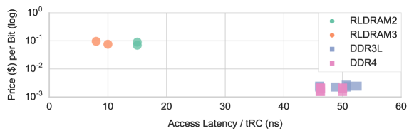
To provide low DRAM access latency, DRAM manufacturers design specialized low-latency DRAM chips (e.g., RLDRAM [235] and FCRAM [297]) at the cost of higher price and lower density than the commonly-used DDRx DRAM (e.g., DDR3 [135], DDR3L [139], DDR4 [137], LPDDR4 [140]) chips. Figure 1.2 compares RLDRAM2/3 (low-latency) to DDR3L/4 DRAM (high-density) chips in terms of cost (i.e., price per bit) and access latency. We obtain the pricing information (for buying a bulk of 1000 DRAM chips) from a major electronic component distributor [77]. Although the RLDRAMx chip attains 4x lower latency than the DDRx DRAM chip, its cost for each bit is significantly higher, 39x. We provide further discussion on how the RLDRAMx chip achieves low latency at a high cost in Section 3.1. One main reason for the high increase in the price is the high area overhead incurred by the architectural designs in RLDRAMx chips. In contrast to the density of a DDRx chip, which ranges from 2Gb to 8Gb, an RLDRAMx chip typically has a low density, ranging from 256Mb to 1.125Gb. Therefore, this dissertation focuses on understanding, characterizing, and addressing the long latency problem of DRAM-based memory systems at low cost (i.e., low DRAM chip area overhead) without intrusive changes to DRAM chips and/or memory controllers.
We first identify three specific problems that cause, incur, or affect long memory latency. First, bulk data movement, the movement of thousands or millions of bytes between two memory locations, is a common operation performed by an increasing number of real-world applications (e.g., [154, 193, 269, 294, 306, 307, 320, 333, 377, 308]). In current systems, since memory is designed as a simple data repository that supplies data, performing a bulk data movement operation between two locations in memory requires the data to go through the processor even though both the source and destination are within the memory. To perform the movement, the data is first read out one cache line at a time from the source location in memory into the processor caches, over a pin-limited off-chip channel (typically 64-bit wide in current systems [57]). Then, the data is written back to memory, again one cache line at a time over the pin-limited channel, into the destination location. By going through the processor, this data movement across memory incurs a significant penalty in terms of both latency and energy consumption (as well as consumed memory bandwidth).
Second, due to the increasing difficulty of efficiently manufacturing smaller DRAM cells with smaller technology nodes, DRAM cells are becoming slower and faultier than they were in the past [252, 243, 165, 159, 155, 229, 168]. At smaller technology nodes, DRAM cells are more susceptible to imperfect manufacturing process, which causes the characteristics (e.g., latency) of the cells to deviate from the DRAM design specification. As a result, latency variation – the phenomenon that cells within the same DRAM chip or across different DRAM chips require different access latencies – becomes a problem in commodity DRAM chips. In order to preserve chip production yield, DRAM manufacturers choose to tolerate latency variation across cells within a chip or from different chips by conservatively setting the standard DRAM latency to be determined by the worst-case latency of any cell in any acceptable chip [192, 57]. This very high worst-case latency is applied uniformly across all DRAM cells in all DRAM chips. As a result, even though some fraction of a DRAM chip and some DRAM chips can inherently be accessed with a latency that is shorter than the standard specification, the standard latency, which is pessimistically set to a very conservative value, prevents systems from attaining higher performance.
Third, since a DRAM cell stores data in a capacitor, which leaks charge over time, DRAM needs to be periodically refreshed to prevent data loss due to leakage. While DRAM is being refreshed, a part of it becomes unavailable to serve memory requests [211, 58], which prolongs the already-long memory latency by delaying the demand requests of processors and accelerators. This problem will become more prevalent as DRAM density increases [211, 58], leading to more DRAM cells to be refreshed within the same refresh interval.
These three problems cause or exacerbate the long memory latency, which is already a critical bottleneck in system performance. The trend of increasing memory latency penalty is expected to continue to grow due to increasing core and accelerator counts (and, hence, increasing memory interference) and the emergence of increasingly more data-intensive and latency-critical applications. Thus, low-latency memory accesses are now even more important than the past on improving overall system performance and energy efficiency.
In addition, there is a critical trade-off between DRAM latency and supply voltage, which greatly affects both the performance and energy efficiency of DRAM chips. There is little experimental understanding of this trade-off and hence almost no mechanisms taking advantage of it in existing systems, which apply a fixed supply voltage value during the runtime. If this voltage-latency trade-off is well understood, one can devise mechanisms that can improve energy efficiency, latency, or both, by achieving a good trade-off depending on system design goals.
1.2 Thesis Statement and Overview
The goal of this thesis is to enable low-latency DRAM memory systems, based on a solid understanding of the causes of and trade-offs related to long DRAM latency. Towards this end, we explore the causes of the three latency problems that we described in the previous section, by (i) examining the internal DRAM chip architecture and memory controller designs, and (ii) experimentally characterizing commodity DRAM chips under various conditions. With the understanding of the causes of long latency, our thesis statement is that
To this end, we (i) propose a series of mechanisms that augment the DRAM chip architecture with simple and low-cost features that better utilize the existing DRAM designs, (ii) develop a better understanding of latency behavior and trade-offs by conducting extensive experiments on real commodity DRAM chips, and (iii) propose techniques to enhance memory controllers to take advantage of the inherent, heterogeneous latency and voltage characteristics of individual DRAM chips employed in the systems rather than treating all the chips as having the same latency. We give a brief overview of our mechanisms and experimental characterizations in the rest of this section.
1.2.1 Low-Cost Inter-Linked Subarrays: Enabling Fast Data Movement
To enable fast and efficient data movement across a wide range of memory at low cost, we propose a new DRAM substrate, Low-Cost Inter-Linked Subarrays (LISA). To achieve this, LISA adds low-cost connections between adjacent subarrays–the smallest building block in today’s DRAM chips. By using these connections to link the existing internal wires (bitlines) of adjacent subarrays, LISA enables wide-bandwidth data transfer across multiple subarrays with only 0.8% DRAM area overhead. As a DRAM substrate, LISA is versatile, enabling an array of new applications that reduce various latency components. We describe and evaluate three such applications in detail: (1) fast inter-subarray bulk data copy, (2) in-DRAM caching using a DRAM architecture whose rows have heterogeneous access latencies, and (3) accelerated bitline precharging (an operation that prepares DRAM for subsequent accesses) by linking multiple precharge units together. Our extensive evaluations show that combining LISA’s three applications attains 1.9x system performance improvement and 2x DRAM energy reduction on average across a variety of workloads running on a quad-core system. To our knowledge, LISA is the first DRAM substrate that supports fast inter-subarray data movement, which enables a wide variety of performance enhancement mechanisms for DRAM systems.
1.2.2 Refresh Parallelization with Memory Accesses
To mitigate the negative performance impact of DRAM refresh, we propose two complementary mechanisms, DARP (Dynamic Access Refresh Parallelization) and SARP (Subarray Access Refresh Parallelization). The goal is to address the drawbacks of per-bank refresh by building more efficient techniques to parallelize refreshes and accesses within DRAM. Per-bank refresh is a state-of-the-art DRAM refresh mechanism that refreshes only a single bank (a bank is a collection of subarrays, and multiple banks are organized into a DRAM chip) at a time. Although per-bank refresh enables a bank to be accessed while another bank is being refreshed, it suffers from two shortcomings that limit the ability of DRAM to serve demand requests while refresh operations are being performed.
First, today’s memory controllers issue per-bank refreshes in a strict round-robin order, which can unnecessarily delay a bank’s demand requests when there are idle banks. To avoid refreshing a bank with pending demand requests, DARP issues per-bank refreshes to idle banks in an out-of-order manner. Furthermore, DRAM writes are not latency-critical because processors do not stall to wait for them. Taking advantage of this observation, DARP proactively schedules refreshes during intervals when a batch of writes are draining to DRAM. Second, SARP exploits the existence of mostly-independent subarrays within a bank. With the cost of only 0.7% DRAM area overhead, it allows a bank to serve memory accesses to an idle subarray while another subarray is being refreshed. Our extensive evaluations on a wide variety of workloads and systems show that our mechanisms improve system performance by 3.3%/7.2%/15.2% on average (and up to 7.1%/14.5%/27.0%) across 100 workloads over per-bank refresh for 8/16/32Gb DRAM chips. To our knowledge, these two techniques are the first mechanisms to (i) enhance refresh scheduling policy of per-bank refresh and (ii) achieve parallelization of refresh and memory accesses within a refreshing bank.
1.2.3 Understanding and Exploiting Latency Variation Within a DRAM Chip
To understand the characteristics of latency variation in modern DRAM chips, we comprehensively characterize 240 DRAM chips from three major vendors and make several new observations about latency variation within DRAM. We find that (i) there is large latency variation across the DRAM cells, and (ii) variation characteristics exhibit significant spatial locality: slower cells are clustered in certain regions of a DRAM chip Based on our observations, we propose Flexible-LatencY DRAM (FLY-DRAM), a mechanism that exploits latency variation across DRAM cells within a DRAM chip to improve system performance. The key idea of FLY-DRAM is to enable the memory controller to exploit the spatial locality of slower cells within DRAM and access the faster DRAM regions with reduced access latency. FLY-DRAM requires modest modification in the memory controller without introducing any changes to the DRAM chips. Our evaluations show that FLY-DRAM improves the performance of a wide range of applications by 13.3%, 17.6%, and 19.5%, on average, for each of the three different vendors’ real DRAM chips, in a simulated 8-core system. To our knowledge, this is the first work to (i) provide a detailed experimental characterization and analysis of latency variation across different cells within a DRAM chip, (ii) show that access latency variation exhibits spatial locality, and (iii) propose mechanisms that take advantage of variation within a DRAM chip to improve system performance.
1.2.4 Understanding and Exploiting Trade-off Between Latency and Voltage Within a DRAM Chip
To understand the critical relationship and trade-off between DRAM latency and supply voltage, which greatly affects both DRAM performance, energy efficiency, and reliability, we perform an experimental study on 124 real DDR3L (low-voltage) DRAM chips manufactured recently by three major DRAM vendors. We find that reducing the supply voltage below a certain point introduces bit errors in the data, and we comprehensively characterize the behavior of these errors. We discover that these errors can be avoided by increasing the access latency. This key finding demonstrates that there exists a trade-off between access latency and supply voltage, i.e., increasing supply voltage enables lower access latency (or vice versa). Based on this trade-off, we propose a new mechanism, Voltron, which aims to improve energy efficiency of DRAM. The key idea of Voltron is to use a performance model to determine how much we can reduce the supply voltage without introducing errors and without exceeding a user-specified threshold for performance loss. Our evaluations show that Voltron reduces the average system energy consumption by 7.3%, with a small system performance loss of 1.8% on average, for a variety of memory-intensive quad-core workloads.
1.3 Contributions
The overarching contribution of this dissertation is the three new mechanisms that reduce DRAM access latency and experimental characterizations for understanding latency behavior in DRAM chips. More specifically, this dissertation makes the following main contributions.
-
1.
We propose a new DRAM substrate, Low-Cost Inter-Linked Subarrays (LISA), which provides high-bandwidth connectivity between subarrays within the same bank to support bulk data movement at low latency, energy, and cost. Using the LISA substrate, we propose and evaluate three new applications: (1) Rapid Inter-Subarray Copy (RISC), which copies data across subarrays at low latency and low DRAM energy; (2) Variable Latency (VILLA) DRAM, which reduces the access latency of frequently-accessed data by caching it in fast subarrays; and (3) Linked Precharge (LIP), which reduces the precharge latency for a subarray by linking its precharge units with neighboring idle precharge units. Chapter 4 describes LISA and its applications in detail.
-
2.
We propose two new refresh mechanisms: (1) DARP (Dynamic Access Refresh Parallelization), a new per-bank refresh scheduling policy, which proactively schedules refreshes to banks that are idle or that are draining writes and (2) SARP (Subarray Access Refresh Parallelization), a new refresh architecture, that enables a bank to serve memory requests in idle subarrays while other subarrays are being refreshed. Chapter 5 describes these two refresh techniques in detail.
-
3.
We experimentally demonstrate and characterize the significant variation in DRAM access latency across different cells within a DRAM chip. Our experimental characterization on modern DRAM chips yields six new fundamental observations about latency variation. Based on this experimentally-driven characterization and understanding, we propose a new mechanism, FLY-DRAM, which exploits the lower latencies of DRAM regions with faster cells by introducing heterogeneous timing parameters into the memory controller. Chapter 6 describes our experiments, analysis, and optimization in detail.
-
4.
We perform a detailed experimental characterization of the effect of varying supply voltage on DRAM latency, reliability, and data retention on real DRAM chips. Our comprehensive experimental characterization provides four major observations on how DRAM latency and reliability is affected by supply voltage. These observations allow us to develop a deep understanding of the critical relationship and trade-off between DRAM latency and supply voltage. Based on this trade-off, we propose a new low-cost DRAM energy optimization mechanism called Voltron, which improves system energy efficiency by dynamically adjusting the voltage based on a performance model. Chapter 7 describes our experiments, analysis, and optimization in detail.
1.4 Outline
This thesis is organized into 8 chapters. Chapter 2 describes necessary background on DRAM organization, operations, and latency. Chapter 3 discusses related prior work on providing low-latency DRAM systems. Chapter 4 presents the design LISA and the three new architectural mechanisms enabled by it. Chapter 5 presents the two new refresh mechanisms (DARP or SARP) that address the refresh interference problem. Chapter 6 presents our experimental study on DRAM latency variation and our mechanism (FLY-DRAM) that exploits it to reduce latency. Chapter 7 presents our experimental study on the trade-off between latency and voltage in DRAM and our mechanism (Voltron) that exploits it to improve energy efficiency. Finally, Chapter 8 presents conclusions and future research directions that are enabled by this dissertation.
Chapter 2 Background
In this chapter, we provide necessary background on DRAM organization and operations used to access data in DRAM. Each operation requires a certain latency, which contributes to the overall DRAM access latency. Understanding of these fundamental operations and their associated latencies provides the core basics required for understanding later chapters in this dissertation.
2.1 High-Level DRAM System Organization
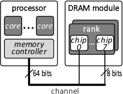
A modern DRAM system consists of a hierarchy of channels, modules, ranks, and chips, as shown in Figure 2.1(a). Each memory channel drives DRAM commands, addresses, and data between a memory controller in the processor and one or more DRAM modules. Each module contains multiple DRAM chips that are organized into one or more ranks. A rank refers to a group of chips that operate in lock step to provide a wide data bus (usually 64 bits), as a single DRAM chip is designed to have a narrow data bus width (usually 8 bits) to minimize chip cost. Each of the eight chips in the rank shown in Figure 2.1(a) transfers 8 bits simultaneously to supply 64 bits of data.
2.2 Internal DRAM Logical Organization
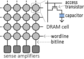
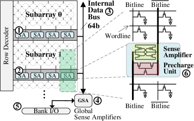
Within a DRAM chip, there are multiple banks (e.g., eight in a typical DRAM chip [135, 172]) that can process DRAM commands independently from each other to increase parallelism. A bank consists of a 2D-array of DRAM cells that are organized into rows and columns, as shown in Figure 2.1(b)111Note that the figure shows a logical representation of the bank to ease the understanding of the DRAM operations required to access data and their associated latency. After we explain the DRAM operations in the next section, we will show the detailed physical organization of a bank in Section 7.1.. A row typically consists of 8K cells. The number of rows varies depending on the chip density. Each DRAM cell has (i) a capacitor that stores binary data in the form of electrical charge (e.g., fully charged and discharged states represent 1 and 0, respectively), and (ii) an access transistor that serves as a switch to connect the capacitor to the bitline. Each column of cells share a bitline, which connects them to a sense amplifier. The sense amplifier senses the charge stored in a cell, converts the charge to digital binary data, and buffers it. Each row of cells share a wire called the wordline, which controls the cells’ access transistors. When a row’s wordline is enabled, the entire row of cells gets connected to the row of sense amplifiers through the bitlines, enabling the sense amplifiers to sense and latch that row’s data. The row of sense amplifiers is also called the row buffer.
2.3 Accessing DRAM
Accessing (i.e., reading from or writing to) a bank consists of three steps: (i) Row Activation & Sense Amplification: opening a row to transfer its data to the row buffer, (ii) Read/Write: accessing the target column in the row buffer, and (iii) Precharge: closing the row and the row buffer. We use Figure 2.2 to explain these three steps in detail. The top part of the figure shows the phase of the cells within the row that is being accessed. The bottom part shows both the DRAM command and data bus timelines, and demonstrates the associated timing parameters.
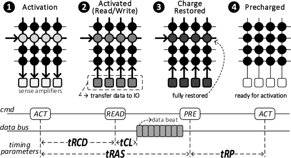
Initial State. Initially, the bank is in the
precharged state ( in Figure 2.2), where
all of the components are ready for activation. All cells are fully charged,
represented with the black color (a darker cell color indicates more
charge). Second, the bitlines are charged to , represented as a thin
line (a thin bitline indicates the initial voltage state of ; a thick
bitline means the bitline is being driven). Third, the wordline is disabled
with V (a thin wordline indicates V; a thick wordline indicates ).
Fourth, the sense amplifier is off without any data latched in it
(indicated by light color in the sense amplifier).
Row Activation & Sense Amplification Phases. To open a row, the
memory controller sends an activate command to raise the wordline of the
corresponding row, which connects the row to the bitlines ( ).
This triggers an activation, where charge starts to flow from the cell to
the bitline (or the other way around, depending on the initial charge level in
the cell) via a process called charge sharing. This process perturbs the
voltage level on the corresponding bitline by a small amount. If the cell is
initially charged (which we assume for the rest of this explanation, without
loss of generality), the bitline voltage is perturbed upwards.
Note that this causes the cell itself to discharge, losing its data temporarily
(hence the lighter color of the accessed row), but this charge will be
restored as we will describe below. After the activation phase, the sense
amplifier senses the voltage perturbation on the bitline, and turns
on to further amplify the voltage level on the bitline by
injecting more charge into the bitline and the cell (making the activated
row’s cells darker in ). When the bitline is amplified to a certain
voltage level (e.g., ), the sense amplifier latches in the cell’s
data, which transforms it into binary data ( ). At this point in
time, the data can be read from the sense amplifier. The latency of these
two phases (activation and sense amplification) is called the
activation latency, and is defined as tRCD in the
standard DDR interface [135, 137]. This activation latency
specifies the latency from the time an activate command is issued to the time
the data is ready to be accessed in the sense amplifier.
Read/Write & Restoration Phases. Once the sense amplifier (row buffer) latches in the data, the memory controller can send a read or write command to access the corresponding column of data within the row buffer (called a column access). The column access time to read the cache line data is called tCL (tCWL for writes). These parameters define the time between the column command and the appearance of the first beat of data on the data bus, shown at the bottom of Figure 2.2. A data beat is a 64-bit data transfer from the DRAM to the processor. In a typical DRAM [135], a column read command reads out 8 data beats (also called an 8-beat burst), thus reading a complete 64-byte cache line.
After the bank becomes activated and the sense amplifier latches in the binary
data of a cell, it starts to restore the connected cell’s charge back to
its original fully-charged state ( ). This phase is known as
restoration, and can happen in parallel with column accesses. The
restoration latency (from issuing an activate command to fully restoring a row of
cells) is defined as tRAS in the standard DDR
interface [135, 137, 172, 193, 192],
as shown in Figure 2.2.
Precharge Phase. In order to access data from a different row, the bank needs to be re-initialized back to the precharged state ( ). To achieve this, the memory controller sends a precharge command, which (i) disables the wordline of the corresponding row, disconnecting the row from the sense amplifiers, and (ii) resets the voltage level on the bitline back to the initial state, , so that the sense amplifier can sense the charge from the new row that is to be opened (i.e., acitviated). The latency of a precharge operation is defined as tRP in the standard DDR interface [135, 137, 172, 193, 192], which is the latency between a precharge and a subsequent activate within the same bank.
2.4 DRAM Refresh
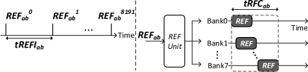
Since the capacitor in a DRAM cell leaks charge over time, to retain data in all cells, DRAM needs to be refreshed periodically [211, 210]. There are two state-of-the-art methods for DRAM refresh: 1) all-bank refresh () and 2) per-bank refresh ().
2.4.1 All-Bank Refresh ()
The minimum time interval during which any cell can retain its electrical charge without being refreshed is called the minimum retention time, which depends on the operating temperature and DRAM type. Because there are tens of thousands of rows in DRAM, refreshing all of them in bulk incurs high latency. Instead, memory controllers send a number of refresh commands that are evenly distributed throughout the retention time to trigger refresh operations, as shown in Figure 2.3(a). Because a typical refresh command in a commodity DDR DRAM chip operates at an entire rank level, it is also called an all-bank refresh or for short [135, 138, 231]. The timeline shows that the time between two commands is specified by (e.g., 7.8s for 64ms retention time). Therefore, refreshing a rank requires refreshes and each operation refreshes exactly of the rank’s rows.
When a rank receives a refresh command, it sends the command to a DRAM-internal refresh unit that selects which specific rows or banks to refresh. A command triggers the refresh unit to refresh a number of rows in every bank for a period of time called (Figure 2.3(a)). During , banks are not refreshed simultaneously. Instead, refresh operations are staggered (pipelined) across banks [241, 58]. The main reason is that refreshing every bank simultaneously would draw more current than what the power delivery network can sustain, leading to potentially incorrect DRAM operation [241, 314]. Because a command triggers refreshes on all the banks within a rank, the entire rank cannot process any memory requests during , The length of is a function of the number of rows to be refreshed.
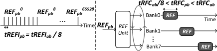
2.4.2 Per-Bank Refresh ()
To allow partial access to DRAM during refresh, LPDDR DRAM (which is designed for mobile platforms), supports an additional, finer-granularity refresh scheme, called per-bank refresh ( for short) [138, 231, 58]. This refresh scheme splits up a operation into eight separate operations scattered across eight banks (Figure 2.3(b)). Therefore, a command is issued eight times more frequently than a command (i.e., = / 8).
Similar to issuing a , a controller simply sends a command to DRAM every without specifying which particular bank to refresh. Instead, when a rank’s internal refresh unit receives a command, it refreshes only one bank for each command following a sequential round-robin order as shown in Figure 2.3(b). The refresh unit inside the DRAM chip uses an internal counter to keep track of which bank to refresh next. The round-robin order is known to the memory controller, so the memory controller knows which bank is being refreshed at any point in time.
By scattering refresh operations from into multiple and non-overlapping per-bank refresh operations, the refresh latency of () becomes shorter than . Disallowing operations from overlapping with each other is a design decision made by the LPDDR3 DRAM standard committee [138]. The reason is simplicity: to avoid the need to introduce new timing constraints, such as the timing between two overlapped refresh operations.222At slightly increased complexity, one can potentially propose a modified standard that allows overlapped refresh of a subset of banks within a rank.
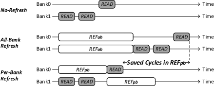
With the support of , LPDDR DRAM can serve memory requests to non-refreshing banks in parallel with a refresh operation in a single bank. Figure 2.4 shows pictorially how provides performance benefits over by enabling the parallelization of refreshes and reads. reduces refresh interference on reads by issuing reads to Bank 1 while Bank 0 is being refreshed. Subsequently, it refreshes Bank 1 while allowing Bank 0 to serve a read at the same time. As a result, alleviates part of the performance loss due to refreshes by enabling parallelization of refreshes and accesses across banks.
2.5 Physical Organization of a DRAM Bank: DRAM Subarrays and Open-Bitline Architecture
In this section, we delve deeper into the physical organization of a bank. This knowledge is required for understanding our proposals described in Chapter 4 and Chapter 5. However, such knowledge is not required for our other two proposals in Chapter 6 and Chapter 7.
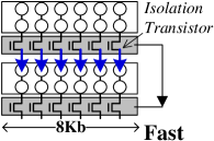
Typically, a bank is subdivided into multiple subarrays [58, 172, 307, 357], as shown in Figure 2.5. Each subarray consists of a 2D-array of DRAM cells that are connected to sense amplifiers through bitlines. Because the size of a sense amplifier is more than 100x the size of a cell [193], modern DRAM designs fit in only enough sense amplifiers in a row to sense half a row of cells. To sense the entire row of cells, each subarray has bitlines that connect to two rows of sense amplifiers — one above and one below the cell array ( and in Figure 2.5, for Subarray 1). This DRAM design is known as the open bitline architecture, and is commonly used to achieve high density in modern DRAM chips [202, 338]. A single row of sense amplifiers, which holds the data from half a row of activated cells, is also referred as a row buffer.
2.5.1 DRAM Subarray Operation
In Section 2.3, we describe the details of major DRAM operations to access data in a bank. In this section, we describe the same set of operations to understand how they work at the subarray-level within a bank. Accessing data in a subarray requires two steps. The DRAM row (typically 8KB across a rank of eight x8 chips) must first be activated. Only after activation completes, a column command (i.e., a read/write) can operate on a piece of data (typically 64B across a rank; the size of a single cache line) from that row.
When an activate command with a row address is issued, the data stored within a row in a subarray is read by two row buffers (i.e., the row buffer at the top of the subarray and the one at the bottom ). First, a wordline corresponding to the row address is selected by the subarray’s row decoder. Then, the top row buffer and the bottom row buffer each sense the charge stored in half of the row’s cells through the bitlines, and amplify the charge to full digital logic values (0 or 1) to latch in the cells’ data.
After an activate finishes latching a row of cells into the row buffers, a read or a write can be issued. Because a typical read/write memory request is made at the granularity of a single cache line, only a subset of bits are selected from a subarray’s row buffer by the column decoder. On a read, the selected column bits are sent to the global sense amplifiers through the internal data bus (also known as the global data lines) , which has a narrow width of 64B across a rank of eight chips (64 bits within a chip). The global sense amplifiers then drive the data to the bank I/O logic , which sends the data out of the DRAM chip to the memory controller.
While the row is activated, a consecutive column command to the same row can access the data from the row buffer without performing an additional activate. This is called a row buffer hit. In order to access a different row in the same bank, a precharge command is required to reinitialize the bitlines’ values for another activate. This re-initialization process is completed by a set of precharge units in the row buffer.
Chapter 3 Related Work
Many prior works propose mechanisms to reduce or mitigate DRAM latency. In this chapter, we describe the closely relevant works by dividing them into different categories based on their high-level approach.
3.1 Specialized Low-Latency DRAM Architecture
RLDRAM [235] and FCRAM [297] enable lower DRAM timing parameters by reducing the length of bitlines (i.e., with a fewer number of cells attached to each bitline). Because the bitline parasitic capacitance reduces with bitline length, shorter bitlines enable faster charge sharing between the cells and the sense amplifiers, thus reducing the latency of DRAM operations [188, 193]. The main drawback of this simple approach is that it leads to lower chip density due to a significant amount of area overhead (30-40% for FCRAM, 40-80% for RLDRAM) induced by the additional peripheral logic (e.g., row decoders) required to support shorter bitlines [172, 193]. In contrast, our proposals do not require as significant and intrusive changes to a DRAM chip.
3.2 Cached DRAM
Several prior works (e.g., [105, 112, 117, 157]) propose to add a small SRAM cache to a DRAM chip to lower the access latency for data that is kept in the SRAM cache (e.g., frequently or recently used data). There are two main disadvantages of these works. First, adding an SRAM cache into a DRAM chip is very intrusive: it incurs a high area overhead (38.8% for 64KB in a 2Gb DRAM chip) and significant design complexity [193, 172]. Second, transferring data from DRAM to SRAM uses a narrow global data bus, internal to the DRAM chip, which is typically 64-bit wide. Thus, installing data into the DRAM cache incurs high latency, especially if the SRAM cache stores data at the row granularity. Compared to these works, our proposals in this dissertation reduce DRAM latency without significant area overhead or complexity.
3.3 Heterogeneous-Latency DRAM
Prior works propose DRAM architectures that provide heterogeneous latency either spatially (dependent on where in the memory an access targets) or temporally (dependent on when an access occurs).
3.3.1 Spatial Heterogeneity
Prior work introduces spatial heterogeneity into DRAM, where one region has a fast access latency but fewer DRAM rows, while the other has a slower access latency but many more rows [193, 320]. The fast region is mainly utilized as a caching area, for the frequently or recently accessed data. We briefly describe two state-of-the-art works that offer different heterogeneous-latency DRAM designs.
CHARM [320] introduces heterogeneity within a rank by designing a few fast banks with (1) shorter bitlines for faster data sensing, and (2) closer placement to the chip I/O for faster data transfers. To exploit these low-latency banks, CHARM uses an OS-managed mechanism to statically map hot data to these banks, based on profiled information from the compiler or programmers. Unfortunately, this approach cannot adapt to program phase changes, limiting its performance gains. If it were to adopt dynamic hot data management, CHARM would incur high migration costs over the narrow 64-bit bus that internally connects the fast and slow banks.
Tiered-Latency DRAM (TL-DRAM) [193] provides heterogeneity within a subarray by dividing the subarray into fast (near) and slow (far) segments that have short and long bitlines, respectively, using isolation transistors. The fast segment can be managed as a software-transparent hardware cache. The main disadvantage is that it needs to cache each hot row in two near segments as each subarray uses two row buffers on opposite ends to sense data in the open-bitline architecture (as we discussed in Section 2.5). This prevents TL-DRAM from using the full near segment capacity. As we can see, neither CHARM nor TL-DRAM strike a good design balance for heterogeneous-latency DRAM. In this dissertation, we propose a new heterogeneous DRAM design that offers fast data movement with a low-cost and easy-to-implement design.
3.3.2 Temporal Heterogeneity
Prior work observes that DRAM latency can vary depending on when an access occurs. The key observation is that a recently-accessed or a recently-refreshed row has nearly full electrical charge in the cells, and thus the following access to the same row can be performed faster [108, 109, 315]. We briefly describe two state-of-the-art works that focus on providing heterogeneous latency temporally.
ChargeCache [108] enables faster access to recently-accessed rows in DRAM by tracking the addresses of recently-accessed rows in the memory controller. NUAT [315] enables accesses to recently-refreshed rows at low latency because these rows are already highly-charged. The main issue with these works is that the proposed effect of highly-charged cells can be accessed with lower latency, is slightly observable only when very long refresh intervals are used on existing DRAM chips, as demonstrated by a recent DRAM characterization work [109]. However, within the duration of the standard 64ms refresh interval, no latency benefits can be directly observed on existing DRAM chips. As a result, these ideas likely require changes to the DRAM chips to provide benefits as suggested by a prior work [109]. In contrast, our work in this dissertation does not require data to be recently-accessed or recently-refreshed to benefit from reduced latency, but it focuses on providing low latency by exploiting spatial heterogeneity. Hence, our techniques are independent of access or refresh patterns.
3.4 Bulk Data Transfer Mechanisms
Prior works [101, 102, 153, 52, 373] propose to add scratchpad memories to reduce CPU pressure during bulk data transfers, which can also enable sophisticated data movement (e.g., scatter-gather), but they still require data to first be moved on-chip. A patent [302] proposes a DRAM design that can copy a page across memory blocks, but lacks concrete analysis and evaluation of the underlying copy operations. Intel I/O Acceleration Technology [123] allows for memory-to-memory DMA transfers across a network, but cannot transfer data within the main memory.
Zhao et al. [377] propose to add a bulk data movement engine inside the memory controller to speed up bulk-copy operations. Jiang et al. [143] design a different copy engine, placed within the cache controller, to alleviate pipeline and cache stalls that occur when these transfers occur. However, these works do not directly address the problem of data movement across the narrow memory channel as they still require the data to move between the main memory and the processor.
Seshadri et al. [307] propose RowClone to perform data movement within a DRAM chip, avoiding costly data transfers over the pin-limited channels. However, its effectiveness is limited because RowClone enables very fast data movement only when the source and destination rows are within the same DRAM subarray. The reason is that while two DRAM rows in the same subarray are connected by row-wide bitlines (e.g., 8K bits), rows in different subarrays are connected through a narrow 64-bit data bus (albeit an internal DRAM bus). Therefore, even for an in-DRAM data movement mechanism such as RowClone, inter-subarray bulk data movement incurs long latency even though data does not move out of the DRAM chip. In contrast, one of our proposals, LISA (Chapter 4), enables fast and energy-efficient bulk data movement across subarrays. We provide more detailed qualitative and quantitative comparisons between LISA and RowClone in Section 4.4.
Lu et al. [214] propose a heterogeneous DRAM design called DAS-DRAM that consists of fast and slow subarrays. It introduces a row of migration cells into each subarray to move rows across different subarrays. Unfortunately, the latency of DAS-DRAM is not scalable with movement distance, because DAS-DRAM requires writing the migrating row into each intermediate subarray’s migration cells before the row reaches its destination, which prolongs the data transfer latency. In contrast, LISA (Chapter 4) provides a direct path to transfer data between row buffers of different subarrays without requiring intermediate data writes into the subarray.
3.5 DRAM Refresh Latency Mitigation
Prior works (e.g., [211, 353, 33, 204, 6, 256, 164, 25, 4, 266, 287, 272]) propose mechanisms to reduce unnecessary refresh operations by taking advantage of the fact that different DRAM cells have widely different retention times [210, 166]. These works assume that the retention time of DRAM cells can be accurately profiled and they depend on having this accurate profile to guarantee data integrity [210]. However, as shown in Liu et al. [210] and later analyzed in detail by several other works [160, 159, 161, 272], accurately determining the retention time profile of DRAM is an outstanding research problem due to the Variable Retention Time (VRT) and Data Pattern Dependence (DPD) phenomena, which can cause the retention time of a cell to fluctuate over time. As such, retention-aware refresh techniques need to overcome the profiling challenges to be viable. A recent work, AVATAR [287], proposes a retention-aware refresh mechanism that addresses VRT by using ECC chips, which introduces extra cost. In contrast, our refresh mitigation techniques (Chapter 5) enable parallelization of refreshes and accesses without relying on cell data retention profiles or ECC, thus reducing the performance overhead of refresh at high reliability and low cost.
Several other works propose different refresh mechanisms. Nair et al. [254] propose Refresh Pausing, which pauses a refresh operation to serve pending memory requests when the refresh causes conflicts with the requests. Although our work already significantly reduces conflicts between refreshes and memory requests by enabling parallelization, it can be combined with Refresh Pausing to address rare conflicts. Tavva et al. [339] propose EFGR, which exposes non-refreshing banks during an all-bank refresh operation so that a few accesses can be scheduled to those non-refreshing banks during the refresh operation. However, such a mechanism does not provide additional performance and energy benefits over state-of-the-art per-bank refresh, which we use to build our mechanism in this dissertation. Isen and John [126] propose ESKIMO, which modifies the ISA to enable memory allocation libraries to skip refreshes on memory regions that do not affect programs’ execution. ESKIMO is orthogonal to our mechanism, and it requires high system-level complexity by requiring system software libraries to make refresh decisions.
Another technique to address refresh latency is through refresh scheduling (e.g., [327, 241, 5, 127, 32]). Stuecheli et al. [327] propose elastic refresh, which postpones refreshes by a time delay that varies based on the number of postponed refreshes and the predicted rank idle time, to avoid interfering with demand requests. Elastic refresh has two shortcomings. First, it becomes less effective when the average rank idle period is shorter than the refresh latency as the refresh latency cannot be fully hidden in that period. This occurs especially with 1) more memory-intensive workloads that inherently have less idleness and 2) higher density DRAM chips that have higher refresh latencies. Second, elastic refresh incurs higher refresh latency when it incorrectly predicts that a period is idle without pending memory requests in the memory controller. In contrast, our mechanisms parallelize refresh operations with accesses even if there is no idle period and they therefore outperform elastic refresh. We quantitatively demonstrate the benefits of our mechanisms over elastic refresh [327] in Section 5.4.
Mukundan et al. [241] propose scheduling techniques to address the problem of command queue seizure, whereby a command queue gets filled up with commands to a refreshing rank, blocking commands to another non-refreshing rank. In our dissertation, we use a different memory controller design that does not have command queues, similarly to another prior work [111, 329, 330, 328]. Our controller generates a command for a scheduled request right before the request is sent to DRAM instead of pre-generating the commands and queueing them up. Thus, our baseline refresh design does not suffer from the problem of command queue seizure.
3.6 Exploiting DRAM Latency Variation
Adaptive-Latency DRAM (AL-DRAM) [192] also characterizes and exploits DRAM latency variation, but does so at a much coarser granularity. This work experimentally characterizes latency variation across different DRAM chips under different operating temperatures. AL-DRAM sets a uniform operation latency for the entire DIMM and does not exploit heterogeneity at the chip-level or within a chip. Chandrasekar et al. study the potential of reducing some DRAM timing parameters [55]. Similar to AL-DRAM, our dissertation observes and characterizes latency variation across DIMMs. Different from prior works, this dissertation also characterizes latency variation within a chip, at the granularity of individual DRAM cells and exploits the latency variation that exists within a DRAM chip. Our proposal can be combined with AL-DRAM to improve performance further.
A recent work by Lee et al. [191, 190] also observes latency variation within DRAM chips. The work analyzes the variation that is due to the circuit design of DRAM components, which it calls design-induced variation. Furthermore, it proposes a new profiling technique to identify the lowest DRAM latency without introducing errors. In this dissertation, we provide the first detailed experimental characterization and analysis of the general latency variation phenomenon within real DRAM chips. Our analysis is broad and is not limited to design-induced variation. Our proposal of exploiting latency variation, FLY-DRAM (Chapter 6), can employ Lee et al.’s new profiling mechanism [191, 190] to identify additional latency variation regions for reducing access latency.
3.7 In-Memory Computation
Modern execution models rely on transferring data from the memory to the processor to perform computation. Since a large number of modern applications consume a large amount of data, this model incurs high latency, bandwidth, and energy due to the excessive use of the narrow memory channel that is typically as wide as only 64 bits. To avoid the memory channel bottleneck, many prior works (e.g., [7, 8, 89, 92, 103, 275, 306, 219, 78, 309, 308, 116, 115, 38, 325, 90, 96, 156, 175, 268, 337, 372, 12, 24, 93, 283, 276, 303]) propose different frameworks and mechanisms to enable processing-in-memory (PIM) to accelerate parts of the applications. However, these works do not fundamentally reduce the raw memory access latency within a DRAM chip. Therefore, our dissertation is complementary to these mechanisms. Furthermore, one of our proposals, LISA (Chapter 4) is also complementary to a previously proposed in-memory bulk processing mechanism that can perform bulk bitwise AND, OR [306, 308]. LISA can enhance the speed and range of such operations as these operations require copying data between rows.
3.8 Mitigating Memory Latency via Memory Scheduling
Since memory has limited bandwidth and parallelism to serve memory requests concurrently, contention for memory bandwidth across different applications can cause significant performance slowdown for individual applications as well as the entire system. Many prior works propose to address bandwidth contention by using more intelligent memory scheduling policies. A number of prior works focus on improving DRAM throughput without being aware of the characteristics of the running applications in the system (e.g., [293, 382, 312, 118, 187]). Many other works observe that application-unaware memory scheduling provides low performance, unfairness, and cases that lead to denial of memory service [238]. As a result, these prior works (e.g., [187, 170, 171, 249, 248, 261, 290, 125, 18, 352, 82, 329, 332, 331, 328, 238, 184, 242, 330, 239, 376, 69, 148]) propose scheduling policies that take into account individual applications’ characteristics to perform better memory request scheduling to improve overall system performance and fairness. While these works reduce the queueing latency experienced by the applications and the system, they do not fundamentally reduce the DRAM access latency of memory requests. The various proposals in this dissertation do, and thus they are complementary to memory scheduling mechanisms.
3.9 Improving Parallelism in DRAM to Hide Memory Latency
A number of prior works propose new DRAM architectures to increase parallelism within DRAM and thus overlap memory latency of different DRAM operations. Kim et al. [172] propose subarray-level parallelism (SALP) to take advantage of the existing subarray architecture to overlap multiple memory requests going to different subarrays within the same bank. O et al. [265] propose to add isolation transistors in each subarray to separate the bitlines from the sense amplifiers, so that the bitlines can be precharged while the row buffer is still activated. Lee et al. [195] propose to add a data channel dedicated for I/O to serve accesses from both the CPU and the I/O subsystem in parallel. Several works [379, 359, 10, 9] propose to divide a DRAM rank into multiple smaller ranks (i.e., sub-ranks) to serve memory requests independently from each sub-rank at the cost of higher read or write latency. All these prior works do not fundamentally reduce the access latency of DRAM operations. Their benefits decrease when more memory accesses interfere with each other at a single subarray, bank, or rank. Our proposals in this dissertation reduce the DRAM access latency directly. These prior works are complementary to our proposals, and combined together with our techniques can provide further system performance improvement.
3.10 Other Prior Works on Mitigating High Memory Latency
3.10.1 Data Prefetching
Many prior works propose data prefetching techniques to load data speculatively from memory into the cache (before the data is accessed), to hide the memory latency with computation (e.g., [184, 310, 187, 262, 323, 180, 15, 26, 51, 68, 83, 150, 119, 149, 66, 84, 81, 245, 250, 244, 106, 185, 107]). However, prefetching does not reduce the fundamental DRAM latency required to fetch data, and prefetch requests can cause interference with demand requests, thereby introducing performance overhead [81, 323, 83]. On the other hand, our proposals can reduce the DRAM access latency for all types of memory requests, without causing interference to other requests.
3.10.2 Multithreading
To hide memory latency, prior works [317, 341, 318, 206, 176, 349] propose to use multithreading to overlap the DRAM latency of one thread with computation by another thread. While multithreading can tolerates the latency experienced by the applications or threads, the technique does not reduce the memory access latency. In fact, multithreading can cause additional delays due to the contention that arises between threads on shared resource accesses. For example, on a GPU system that runs a large number of threads, memory latency can still be a performance limiter when threads stalling on memory requests delay other threads from being issued [147, 355, 146, 258, 20]. Exploiting the potential of multithreading provided by the hardware also requires non-trivial effort from programmers to write bug-free programs [196]. Furthermore, multithreading does not improve single-thread performance, which is still important for many modern applications, e.g., mobile applications [104]. Critical threads that are delayed on a memory access can be bottlenecks that degrade the performance of an entire multi-threaded application by delaying other threads [82, 335, 144, 145, 334, 79]. Our proposals in this dissertation reduce the memory access latency directly. As a result, these proposals not only improve single-thread performance but also the performance of multithreading processors by reducing the amount of memory stall time of critical threads that can stall other threads.
3.10.3 Processor Architecture Design to Tolerate Memory Latency
A single processor core can employ various techniques to tolerate memory latency by generating multiple DRAM accesses that can potentially be served concurrently by the DRAM system (e.g., out-of-order execution [346, 274], non-blocking caches [178], and runahead execution [245, 250, 244, 107, 251, 247]). The effectiveness of these latency tolerance techniques highly depends on whether DRAM can serve the generated memory accesses in parallel as these techniques do not directly reduce the latency of individual accesses.
Other prior works (e.g. [246, 209, 208, 298, 367, 342, 244, 358]) propose to use value prediction to avoid pipeline stalls due to memory by predicting the requested data value. However, incorrect value prediction incurs high cost due to pipeline flushes and re-executions. Although this cost can be mitigated with approximate value prediction [367, 342], approximation is not applicable to all applications as some require precise correctness for execution.
Our proposals in this dissertation directly reduce DRAM access latency even if the accesses cannot be served in parallel. Our proposals are also complementary to these processor architectural techniques as we introduce low-cost modifications to DRAM chips and memory controllers.
3.10.4 System Software to Mitigate Application Interference
Prior works (e.g., [163, 213, 162, 80, 212, 205, 381]) propose system software techniques to manage inter-application interference in the memory to reduce interference-induced memory latency. These works do not reduce the access latency to memory. However, their techniques are complementary to our proposals.
3.10.5 Reducing Latency of On-Chip Interconnects
Prior works (e.g. [362, 61, 69, 100, 71, 313, 70, 197, 88, 99, 98, 240, 87]) propose mechanisms to reduce the latency of memory requests when they are traversing the on-chip interconnects. These works are complementary to the proposals presented in this dissertation since our works reduce the fundamental memory device access latency.
3.10.6 Reducing Latency of Non-Volatile Memory
In this dissertation, we focus on the DRAM technology, which is the predominant physical substrate for main memory in today’s systems. On the other hand, a new class of non-volatile memory (NVM) technology is becoming a potential substrate to replace DRAM or co-exist with DRAM in future systems [227, 179, 226, 368, 288, 286, 181, 183, 182]. Since NVM has substantially longer latency than DRAM, prior works (e.g., [255, 369, 227, 179, 113, 201, 284, 374, 141, 181, 183, 182]) propose various techniques to reduce the access latency of different types of NVM (e.g., PCM and STT-RAM). However, these techniques are not directly applicable to DRAM devices because each NVM technology has a fundamentally different way of accessing its memory cells (i.e., devices) from DRAM.
3.11 Experimental Studies of Memory Chips
In this dissertation, we provide extensive detailed experimental characterization and analysis of latency behavior in modern commodity DRAM chips. There have been other experimental studies of DRAM chips [109, 161, 55, 152, 151, 192, 168, 210, 160, 159, 272, 190, 191, 189, 167] that study various issues including data retention, read disturbance, latency, address mapping, and power. There have also been field studies of the characteristics of DRAM memories employed in large-scale systems [85, 120, 301, 229, 199, 322, 321]. Both of these types works are complementary to the works presented in this dissertation.
Similarly, there have been experimental studies of other types of memories, especially NAND flash memory [44, 271, 217, 47, 50, 48, 43, 49, 46, 45, 41, 40, 91]. These studies develop a similar FPGA-based infrastructure [42, 91] used in this dissertation and examine various issues including data retention, read disturbance, latency, P/E cycling errors, programming errors, and cell-to-cell program interference. There have also been field studies of the characteristics of flash memories employed in large-scale systems [228, 300, 270, 259]. These works are also complementary to the experimental works presented in this dissertation.
Chapter 4 Low-Cost Inter-Linked Subarrays (LISA)
Bulk data movement, the movement of thousands or millions of bytes between two memory locations, is a common operation performed by an increasing number of real-world applications (e.g., [154, 193, 269, 294, 306, 307, 320, 333, 377]). Therefore, it has been the target of several architectural optimizations (e.g., [35, 143, 307, 360, 377]). In fact, bulk data movement is important enough that modern commercial processors are adding specialized support to improve its performance, such as the ERMSB instruction recently added to the x86 ISA [124].
In today’s systems, to perform a bulk data movement between two locations in memory, the data needs to go through the processor even though both the source and destination are within memory. To perform the movement, the data is first read out one cache line at a time from the source location in memory into the processor caches, over a pin-limited off-chip channel (typically 64 bits wide). Then, the data is written back to memory, again one cache line at a time over the pin-limited channel, into the destination location. By going through the processor, this data movement incurs a significant penalty in terms of latency and energy consumption. In this chapter, we introduce a new DRAM substrate, Low-Cost Inter-Linked Subarrays (LISA), whose goal is to enable fast and efficient data movement across a large range of memory at low cost. We show that, as a DRAM substrate, LISA is versatile, enabling an array of new applications that reduce the fundamental access latency of DRAM.
4.1 Motivation: Low Subarray Connectivity Inside DRAM
To address the inefficiencies of traversing the pin-limited channel, a number of mechanisms have been proposed to accelerate bulk data movement (e.g., [143, 214, 307, 377]). The state-of-the-art mechanism, RowClone [307], performs data movement completely within a DRAM chip, avoiding costly data transfers over the pin-limited memory channel. However, its effectiveness is limited because RowClone can enable fast data movement only when the source and destination are within the same DRAM subarray. A DRAM chip is divided into multiple banks (typically 8), each of which is further split into many subarrays (16 to 64) [172], shown in Figure 4.1, to ensure reasonable read and write latencies at high density [58, 135, 137, 172, 350]. Each subarray is a two-dimensional array with hundreds of rows of DRAM cells, and contains only a few megabytes of data (e.g., 4MB in a rank of eight 1Gb DDR3 DRAM chips with 32 subarrays per bank). While two DRAM rows in the same subarray are connected via a wide (e.g., 8K bits) bitline interface, rows in different subarrays are connected via only a narrow 64-bit data bus within the DRAM chip (Figure 4.1). Therefore, even for previously-proposed in-DRAM data movement mechanisms such as RowClone [307], inter-subarray bulk data movement incurs long latency and high memory energy consumption even though data does not move out of the DRAM chip.
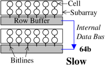
While it is clear that fast inter-subarray data movement can have several applications that improve system performance and memory energy efficiency [154, 269, 294, 306, 307, 377], there is currently no mechanism that performs such data movement quickly and efficiently. This is because no wide datapath exists today between subarrays within the same bank (i.e., the connectivity of subarrays is low in modern DRAM). Our goal is to design a low-cost DRAM substrate that enables fast and energy-efficient data movement across subarrays.
4.2 Design Overview and Applications of LISA
We make two key observations that allow us to improve the connectivity of subarrays within each bank in modern DRAM. First, accessing data in DRAM causes the transfer of an entire row of DRAM cells to a buffer (i.e., the row buffer, where the row data temporarily resides while it is read or written) via the subarray’s bitlines. Each bitline connects a column of cells to the row buffer, interconnecting every row within the same subarray (Figure 4.1). Therefore, the bitlines essentially serve as a very wide bus that transfers a row’s worth of data (e.g., 8K bits) at once. Second, subarrays within the same bank are placed in close proximity to each other. Thus, the bitlines of a subarray are very close to (but are not currently connected to) the bitlines of neighboring subarrays (as shown in Figure 4.1).
Key Idea. Based on these two observations, we introduce a new DRAM substrate, called Low-cost Inter-linked SubArrays (LISA). LISA enables low-latency, high-bandwidth inter-subarray connectivity by linking neighboring subarrays’ bitlines together with isolation transistors, as illustrated in Figure 4.1. We use the new inter-subarray connection in LISA to develop a new DRAM operation, row buffer movement (RBM), which moves data that is latched in an activated row buffer in one subarray into an inactive row buffer in another subarray, without having to send data through the narrow internal data bus in DRAM. RBM exploits the fact that the activated row buffer has enough drive strength to induce charge perturbation within the idle (i.e., precharged) bitlines of neighboring subarrays, allowing the destination row buffer to sense and latch this data when the isolation transistors are enabled.
By using a rigorous DRAM circuit model that conforms to the JEDEC standards [135] and ITRS specifications [131, 132], we show that RBM performs inter-subarray data movement at 26x the bandwidth of a modern 64-bit DDR4-2400 memory channel (500 GB/s vs. 19.2 GB/s; see §4.3.3), even after we conservatively add a large (60%) timing margin to account for process and temperature variation.
Applications of LISA. We exploit LISA’s fast inter-subarray movement to enable many applications that can improve system performance and energy efficiency. We implement and evaluate the following three applications of LISA:
-
•
Bulk data copying. Fast inter-subarray data movement can eliminate long data movement latencies for copies between two locations in the same DRAM chip. Prior work showed that such copy operations are widely used in today’s operating systems [269, 294] and datacenters [154]. We propose Rapid Inter-Subarray Copy (RISC), a new bulk data copying mechanism based on LISA’s RBM operation, to reduce the latency and DRAM energy of an inter-subarray copy by 9.2x and 48.1x, respectively, over the best previous mechanism, RowClone [307] (§4.4).
-
•
Enabling access latency heterogeneity within DRAM. Prior works [193, 320] introduced non-uniform access latencies within DRAM, and harnessed this heterogeneity to provide a data caching mechanism within DRAM for hot (i.e., frequently-accessed) pages. However, these works do not achieve either one of the following goals: (1) low area overhead, and (2) fast data movement from the slow portion of DRAM to the fast portion. By exploiting the LISA substrate, we propose a new DRAM design, VarIabLe LAtency (VILLA) DRAM, with asymmetric subarrays that reduce the access latency to hot rows by up to 63%, delivering high system performance and achieving both goals of low overhead and fast data movement (§4.5).
-
•
Reducing precharge latency. Precharge is the process of preparing the subarray for the next memory access [135, 172, 192, 193]. It incurs latency that is on the critical path of a bank-conflict memory access. The precharge latency of a subarray is limited by the drive strength of the precharge unit attached to its row buffer. We demonstrate that LISA enables a new mechanism, LInked Precharge (LIP), which connects a subarray’s precharge unit with the idle precharge units in the neighboring subarrays, thereby accelerating precharge and reducing its latency by 2.6x (§4.6).
These three mechanisms are complementary to each other, and we show that when combined, they provide additive system performance and energy efficiency improvements (§4.9.4). LISA is a versatile DRAM substrate, capable of supporting several other applications beyond these three, such as performing efficient data remapping to avoid conflicts in systems that support subarray-level parallelism [172], and improving the efficiency of bulk bitwise operations in DRAM [306] (see §4.10).
4.3 Mechanism
First, we discuss the low-cost design changes to DRAM to enable high-bandwidth connectivity across neighboring subarrays (Section 4.3.1). We then introduce a new DRAM command that uses this new connectivity to perform bulk data movement (Section 4.3.2). Finally, we conduct circuit-level studies to determine the latency of this command (Sections 4.3.3 and 4.3.4).
4.3.1 LISA Design in DRAM
LISA is built upon two key characteristics of DRAM. First, large data bandwidth within a subarray is already available in today’s DRAM chips. A row activation transfers an entire DRAM row (e.g., 8KB across all chips in a rank) into the row buffer via the bitlines of the subarray. These bitlines essentially serve as a wide bus that transfers an entire row of data in parallel to the respective subarray’s row buffer. Second, every subarray has its own set of bitlines, and subarrays within the same bank are placed in close proximity to each other. Therefore, a subarray’s bitlines are very close to its neighboring subarrays’ bitlines, although these bitlines are not directly connected together.111Note that matching the bitline pitch across subarrays is important for a high-yield DRAM process [202, 338].
By leveraging these two characteristics, we propose to build a wide connection path between subarrays within the same bank at low cost, to overcome the problem of a narrow connection path between subarrays in commodity DRAM chips (i.e., the internal data bus in Figure 2.5). Figure 4.2 shows the subarray structures in LISA. To form a new, low-cost inter-subarray datapath with the same wide bandwidth that already exists inside a subarray, we join neighboring subarrays’ bitlines together using isolation transistors. We call each of these isolation transistors a link. A link connects the bitlines for the same column of two adjacent subarrays.
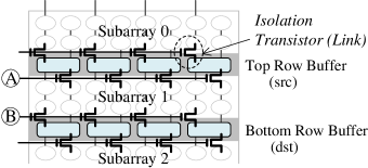
When the isolation transistor is turned on (i.e., the link is enabled), the bitlines of two adjacent subarrays are connected. Thus, the sense amplifier of a subarray that has already driven its bitlines (due to an activate) can also drive its neighboring subarray’s precharged bitlines through the enabled link. This causes the neighboring sense amplifiers to sense the charge difference, and simultaneously help drive both sets of bitlines. When the isolation transistor is turned off (i.e., the link is disabled), the neighboring subarrays are disconnected from each other and thus operate as in conventional DRAM.
4.3.2 Row Buffer Movement (RBM) Through LISA
Now that we have inserted physical links to provide high-bandwidth connections across subarrays, we must provide a way for the memory controller to make use of these new connections. Therefore, we introduce a new DRAM command, RBM, which triggers an operation to move data from one row buffer (half a row of data) to another row buffer within the same bank through these links. This operation serves as the building block for our architectural optimizations.
To help explain the RBM process between two row buffers, we assume that the top row buffer and the bottom row buffer in Figure 4.2 are the source (src) and destination (dst) of an example RBM operation, respectively, and that src is activated with the content of a row from Subarray 0. To perform this RBM, the memory controller enables the links ( and ) between src and dst, thereby connecting the two row buffers’ bitlines together ( of src to of dst, and of src to of dst).
Figure 4.3 illustrates how RBM drives the data from src to dst. For clarity, we show only one column from each row buffer. State shows the initial values of the bitlines ( and ) attached to the row buffers — src is activated and has fully driven its bitlines (indicated by thick bitlines), and dst is in the precharged state (thin bitlines indicating a voltage state of ). In state , the links between src and dst are turned on. The charge of the src bitline () flows to the connected bitline () of dst, raising the voltage level of dst’s to . The other bitlines () have the opposite charge flow direction, where the charge flows from the of dst to the of src. This phase of charge flowing between the bitlines is known as charge sharing. It triggers dst’s row buffer to sense the increase of differential voltage between and , and amplify the voltage difference further. As a result, both src and dst start driving the bitlines with the same values. This double sense amplification process pushes both sets of bitlines to reach the final fully sensed state ( ), thus completing the RBM from src to dst.
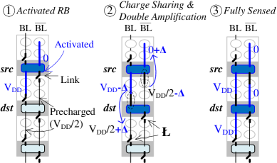
Extending this process, RBM can move data between two row buffers that are not adjacent to each other as well. For example, RBM can move data from the src row buffer (in Figure 4.2) to a row buffer, dst2, that is two subarrays away (i.e., the bottom row buffer of Subarray 2, not shown in Figure 4.2). This operation is similar to the movement shown in Figure 4.3, except that the RBM command turns on two extra links ( in Figure 4.3), which connect the bitlines of dst to the bitlines of dst2, in state . By enabling RBM to perform row buffer movement across non-adjacent subarrays via a single command, instead of requiring multiple commands, the movement latency and command bandwidth are reduced.
4.3.3 Row Buffer Movement (RBM) Latency
To validate the RBM process over LISA links and evaluate its latency, we build a model of LISA using the Spectre Circuit Simulator [39], with the NCSU FreePDK 45nm library [263]. We configure the DRAM using the JEDEC DDR3-1600 timings [135], and attach each bitline to 512 DRAM cells [193, 320]. We conservatively perform our evaluations using worst-case cells, with the resistance and capacitance parameters specified in the ITRS reports [131, 132] for the metal lanes. Furthermore, we conservatively model the worst RC drop (and hence latency) by evaluating cells located at the edges of subarrays.
We now analyze the process of using one RBM operation to move data between two non-adjacent row buffers that are two subarrays apart. To help the explanation, we use an example that performs RBM from RB0 to RB2, as shown on the left side of Figure 4.4. The right side of the figure shows the voltage of a single bitline from each subarray during the RBM process over time. The voltage of the bitlines show the same behavior, but have inverted values. We now explain this RBM process step by step.
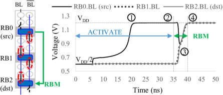
First, before the RBM command is issued, an activate command is sent to RB0 at time 0. After roughly 21ns ( ), the bitline reaches , which indicates the cells have been fully restored (tRAS). Note that, in our simulation, restoration happens more quickly than the standard-specified tRAS value of 35ns, as the standard includes a guardband on top of the typical cell restoration time to account for process and temperature variation [55, 192]. This amount of margin is on par with values experimentally observed in commodity DRAMs at 55°C [192].
Second, at 35ns ( ), the memory controller sends the RBM command to move data from RB0 to RB2. RBM simultaneously turns on the four links (circled on the left in Figure 4.4) that connect the subarrays’ bitlines.
Third, after a small amount of time ( ), the voltage of RB0’s bitline drops to about 0.9V, as the fully-driven bitlines of RB0 are now charge sharing with the precharged bitlines attached to RB1 and RB2. This causes both RB1 and RB2 to sense the charge difference and start amplifying the bitline values. Finally, after amplifying the bitlines for a few nanoseconds ( at 40ns), all three bitlines become fully driven with the value that is originally stored in RB0.
We thus demonstrate that RBM moves data from one row buffer to a row buffer two subarrays away at very low latency. Our SPICE simulation shows that the RBM latency across two LISA links is approximately 5ns ( ). To be conservative, we do not allow data movement across more than two subarrays with a single RBM command.222In other words, RBM has two variants, one that moves data between immediately adjacent subarrays (Figure 4.3) and one that moves data between subarrays that are one subarray apart from each other (Figure 4.4).
4.3.4 Handling Process and Temperature Variation
On top of using worst-case cells in our SPICE model, we add in a latency guardband to the RBM latency to account for process and temperature variation, as DRAM manufacturers commonly do [55, 192]. For instance, the activate timing (tRCD) has been observed to have margins of 13.3% [55] and 17.3% [192] for different types of commodity DRAMs. To conservatively account for process and temperature variation in LISA, we add a large timing margin, of 60%, to the RBM latency. Even then, RBM latency is 8ns and RBM provides a 500 GB/s data transfer bandwidth across two subarrays that are one subarray apart from each other, which is 26x the bandwidth of a DDR4-2400 DRAM channel (19.2 GB/s) [137].
4.4 Application 1: Rapid Inter-Subarray Bulk Data Copying (LISA-RISC)
Due to the narrow memory channel width, bulk copy operations used by applications and operating systems are performance limiters in today’s systems [143, 154, 307, 377]. These operations are commonly performed due to the memcpy and memmov. Recent work reported that these two operations consume 4-5% of all of Google’s datacenter cycles, making them an important target for lightweight hardware acceleration [154]. As we show in Section 4.4.1, the state-of-the-art solution, RowClone [307], has poor performance for such operations when they are performed across subarrays in the same bank.
Our goal is to provide an architectural mechanism to accelerate these inter-subarray copy operations in DRAM. We propose LISA-RISC, which uses the RBM operation in LISA to perform rapid data copying. We describe the high-level operation of LISA-RISC (Section 4.4.2), and then provide a detailed look at the memory controller command sequence required to implement LISA-RISC (Section 4.4.3).
4.4.1 Shortcomings of the State-of-the-Art
Previously, we have described the state-of-the-art work, RowClone [307], which addresses the problem of costly data movement over memory channels by coping data completely in DRAM. However, RowClone does not provide fast data copy between subarrays. The main latency benefit of RowClone comes from intra-subarray copy (RC-IntraSA for short) as it copies data at the row granularity. In contrast, inter-subarray RowClone (RC-InterSA) requires transferring data at the cache line granularity (64B) through the internal data bus in DRAM. Consequently, RC-InterSA incurs 16x longer latency than RC-IntraSA. Furthermore, RC-InterSA is a long blocking operation that prevents reading from or writing to the other banks in the same rank, reducing bank-level parallelism [187, 249].
To demonstrate the ineffectiveness of RC-InterSA, we compare it to today’s currently-used copy mechanism, memcpy, which moves data via the memory channel. In contrast to RC-InterSA, which copies data in DRAM, memcpy copies data by sequentially reading out source data from the memory and then writing it to the destination data in the on-chip caches. Figure 4.5 compares the average system performance and queuing latency of RC-InterSA and memcpy, on a quad-core system across 50 workloads that contain bulk (8KB) data copies (see Section 4.8 for our methodology). RC-InterSA actually degrades system performance by 24% relative to memcpy, mainly because RC-InterSA increases the overall memory queuing latency by 2.88x, as it blocks other memory requests from being serviced by the memory controller performing the RC-InterSA copy. In contrast, memcpy is not a long or blocking DRAM command, but rather a long sequence of memory requests that can be interrupted by other critical memory requests, as the memory scheduler can issue memory requests out of order [170, 171, 248, 249, 293, 329, 352, 382].
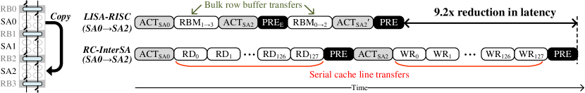
On the other hand, RC-InterSA offers energy savings of 5.1% on average over memcpy by not transferring the data over the memory channel. Overall, these results show that neither of the existing mechanisms (memcpy or RowClone) offers fast and energy-efficient bulk data copy across subarrays.
4.4.2 In-DRAM Rapid Inter-Subarray Copy (RISC)
Our goal is to design a new mechanism that enables low-latency and energy-efficient memory copy between rows in different subarrays within the same bank. To this end, we propose a new in-DRAM copy mechanism that uses LISA to exploit the high-bandwidth links between subarrays. The key idea, step by step, is to: (1) activate a source row in a subarray; (2) rapidly transfer the data in the activated source row buffers to the destination subarray’s row buffers, through LISA’s wide inter-subarray links, without using the narrow internal data bus; and (3) activate the destination row, which enables the contents of the destination row buffers to be latched into the destination row. We call this inter-subarray row-to-row copy mechanism LISA-Rapid Inter-Subarray Copy (LISA-RISC).
As LISA-RISC uses the full row bandwidth provided by LISA, it reduces the copy latency by 9.2x compared to RC-InterSA (see Section 4.4.5). An additional benefit of using LISA-RISC is that its inter-subarray copy operations are performed completely inside a bank. As the internal DRAM data bus is untouched, other banks can concurrently serve memory requests, exploiting bank-level parallelism. This new mechanism is complementary to RowClone, which performs fast intra-subarray copies. Together, our mechanism and RowClone can enable a complete set of fast in-DRAM copy techniques in future systems. We now explain the step-by-step operation of how LISA-RISC copies data across subarrays.
4.4.3 Detailed Operation of LISA-RISC
Figure 4.6 shows the command service timelines for both LISA-RISC and RC-InterSA, for copying a single row of data across two subarrays, as we show on the left. Data is copied from subarray SA0 to SA2. We illustrate four row buffers (RB0–RB3): recall from Section 2.5 that in order to activate one row, a subarray must use two row buffers (at the top and bottom), as each row buffer contains only half a row of data. As a result, LISA-RISC must copy half a row at a time, first moving the contents of RB1 into RB3, and then the contents of RB0 into RB2, using two RBM commands.
First, the LISA-RISC memory controller activates the source row (ACTSA0) to latch its data into two row buffers (RB0 and RB1). Second, LISA-RISC invokes the first RBM operation (RBM13) to move data from the bottom source row buffer (RB1) to the respective destination row buffer (RB3), thereby linking RB1 to both RB2 and RB3, which activates both RB2 and RB3. After this step, LISA-RISC cannot immediately invoke another RBM to transfer the remaining half of the source row in RB0 into RB2, as a row buffer (RB2) needs to be in the precharged state in order to receive data from an activated row buffer (RB0). Therefore, LISA-RISC completes copying the first half of the source data into the destination row before invoking the second RBM, by writing the row buffer (RB3) into the cells through an activation (ACTSA2). This activation enables the contents of the sense amplifiers (RB3) to be driven into the destination row. To address the issue that modern DRAM chips do not allow a second activate to an already-activated bank, we use the back-to-back activate command that is used to support RowClone [307].
Third, to move data from RB0 to RB2 to complete the copy transaction, we need to precharge both RB1 and RB2. The challenge here is to precharge all row buffers except RB0. This cannot be accomplished in today’s DRAM because a precharge is applied at the bank level to all row buffers. Therefore, we propose to add a new precharge-exception command, which prevents a row buffer from being precharged and keeps it activated. This bank-wide exception signal is supplied to all row buffers, and when raised for a particular row buffer, the selected row buffer retains its state while the other row buffers are precharged. After the precharge-exception (PREE) is complete, we then invoke the second RBM (RBM02) to copy RB0 to RB2, which is followed by an activation (ACTSA2´) to write RB2 into SA2. Finally, LISA-RISC finishes the copy by issuing a precharge command (PRE in Figure 4.6) to the bank.
In comparison, the command service timeline of RC-InterSA is much longer, as RowClone can copy only one cache line of data at a time (as opposed to half a row buffer). This requires 128 serial cache line transfers to read the data from RB0 and RB1 into a temporary row in another bank, followed by another 128 serial cache line transfers to write the data into RB2 and RB3. LISA-RISC, by moving half a row using a single RBM command, achieves 9.2x lower latency than RC-InterSA.
4.4.4 Data Coherence
When a copy is performed in DRAM, one potential disadvantage is that the data stored in the DRAM may not be the most recent version, as the processor may have dirty cache lines that belong to the section of memory being copied. Prior works on in-DRAM migration have proposed techniques to accommodate data coherence [306, 307]. Alternatively, we can accelerate coherence operations by using structures like the Dirty-Block Index [304].
4.4.5 Comparison of Copy Techniques
Figure 4.7 shows the DRAM latency and DRAM energy consumption of different copy commands for copying a row of data (8KB). The exact latency and energy numbers are listed in Table 4.1.333Our reported numbers differ from prior work [307] because: (1) we use faster DRAM timing parameters (1600-11-11-11 vs 1066-8-8-8), and (2) we use the 8KB row size of most commercial DRAM instead of 4KB [307]. We derive the copy latency of each command sequence using equations based on the DDR3-1600 timings [135] (available in our technical report [59]), and the DRAM energy using the Micron power calculator [230]. For LISA-RISC, we define a hop as the number of subarrays that LISA-RISC needs to copy data across to move the data from the source subarray to the destination subarray. For example, if the source and destination subarrays are adjacent to each other, the number of hops is 1. The DRAM chips that we evaluate have 16 subarrays per bank, so the maximum number of hops is 15.
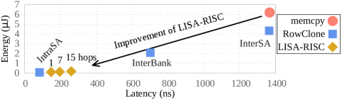
| Copy Commands (8KB) | Latency (ns) | Energy (J) |
|---|---|---|
| memcpy (via mem. channel) | 1366.25 | 6.2 |
| RC-InterSA / Bank / IntraSA | 1363.75 / 701.25 / 83.75 | 4.33 / 2.08 / 0.06 |
| LISA-RISC (1 / 7 / 15 hops) | 148.5 / 196.5 / 260.5 | 0.09 / 0.12 / 0.17 |
We make two observations from these numbers. First, although RC-InterSA incurs similar latencies as memcpy, it consumes 29.6% less energy, as it does not transfer data over the channel and DRAM I/O for each copy operation. However, as we showed in Section 4.4.1, RC-InterSA incurs a higher system performance penalty because it is a long-latency blocking memory command. Second, copying between subarrays using LISA achieves significantly lower latency and energy compared to RowClone, even though the total latency of LISA-RISC grows linearly with the hop count.
By exploiting the LISA substrate, we thus provide a more complete set of in-DRAM copy mechanisms. Our workload evaluation results show that LISA-RISC outperforms RC-InterSA and memcpy: its average performance improvement and energy reduction over the best performing inter-subarray copy mechanism (i.e., memcpy) are 66.2% and 55.4%, respectively, on a quad-core system, across 50 workloads that perform bulk copies (see Section 4.9.1).
4.5 Application 2: In-DRAM Caching Using Heterogeneous Subarrays (LISA-VILLA)
Our second application aims to reduce the DRAM access latency for frequently-accessed (hot) data. Prior work introduces heterogeneity into DRAM, where one region has a fast access latency but small capacity (fewer DRAM rows), while the other has a slow access latency but high capacity (many more rows) [193, 320]. To yield the highest performance benefits, the fast region is used as a dynamic cache that stores the hot rows. There are two design constraints that must be considered: (1) ease of implementation, as the fast caching structure needs to be low-cost and non-intrusive; and (2) data movement cost, as the caching mechanism should adapt to dynamic program phase changes, which can lead to changes in the set of hot DRAM rows. As we show in Section 4.5.1, prior work has not balanced the trade-off between these two constraints.
Our goal is to design a heterogeneous DRAM that offers fast data movement with a low-cost and easy-to-implement design. To this end, we propose LISA-VILLA (VarIabLe LAtency), a mechanism that uses LISA to provide fast row movement into the cache when the set of hot DRAM rows changes. LISA-VILLA is also easy to implement, as discussed in Section 4.5.2. We describe our hot row caching policy in Section 4.5.3.
4.5.1 Shortcomings of the State-of-the-Art
We observe that two state-of-the-art techniques for heterogeneity within a DRAM chip are not effective at providing both ease of implementation and low movement cost.
CHARM [320] introduces heterogeneity within a rank by designing a few fast banks with (1) shorter bitlines for faster data sensing, and (2) closer placement to the chip I/O for faster data transfers. To exploit these low-latency banks, CHARM uses an OS-managed mechanism to statically allocate hot data to them based on program profile information. Unfortunately, this approach cannot adapt to program phase changes, limiting its performance gains. If it were to adopt dynamic hot data management, CHARM would incur high movement cost over the narrow 64-bit internal data bus in DRAM, as illustrated in Figure 4.8(a), since it does not provide high-bandwidth connectivity between banks.
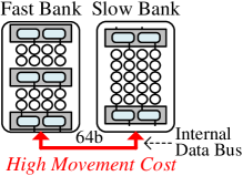
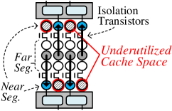
TL-DRAM [193] provides heterogeneity within a subarray by dividing it into fast (near) and slow (far) segments that have short and long bitlines, respectively, using isolation transistors. To manage the fast segment as an OS-transparent hardware cache, TL-DRAM proposes a fast intra-subarray movement scheme similar to RowClone [307]. The main disadvantage is that TL-DRAM needs to cache each hot row in two near segments, as shown in Figure 4.8(b), as each subarray uses two row buffers on opposite ends to sense data in the open-bitline architecture. This prevents TL-DRAM from using the full near segment capacity. TL-DRAM’s area overhead is also sizable (3.15%) in an open-bitline architecture. As we can see, neither CHARM nor TL-DRAM strike a good trade-off between the two design constraints.
4.5.2 Variable Latency (VILLA) DRAM
We propose to introduce heterogeneity within a bank by designing heterogeneous-latency subarrays. We call this heterogeneous DRAM design VarIabLe LAtency DRAM (VILLA-DRAM). To design a low-cost fast subarray, we take an approach similar to prior work, attaching fewer cells to each bitline to reduce the parasitic capacitance and resistance. This reduces the sensing (tRCD), restoration (tRAS), and precharge (tRP) time of the fast subarrays [193, 235, 320]. In this chapter, we focus on managing the fast subarrays in hardware, as it offers better adaptivity to dynamic changes in the hot data set.
In order to take advantage of VILLA-DRAM, we rely on LISA-RISC to rapidly copy rows across subarrays, which significantly reduces the caching latency. We call this synergistic design, which builds VILLA-DRAM using the LISA substrate, LISA-VILLA. Nonetheless, the cost of transferring data to a fast subarray is still non-negligible, especially if the fast subarray is far from the subarray where the data to be cached resides. Therefore, an intelligent cost-aware mechanism is required to make astute decisions on which data to cache and when.
4.5.3 Caching Policy for LISA-VILLA
We design a simple epoch-based caching policy to evaluate the benefits of caching a row in LISA-VILLA. Every epoch, we track the number of accesses to rows by using a set of 1024 saturating counters for each bank.444The hardware cost of these counters is low, requiring only 6KB of storage in the memory controller (see Section 4.7.1). The counter values are halved every epoch to prevent staleness. At the end of an epoch, we mark the 16 most frequently-accessed rows as hot, and cache them when they are accessed the next time. For our cache replacement policy, we use the benefit-based caching policy proposed by Lee et al. [193]. Specifically, it uses a benefit counter for each row cached in the fast subarray: whenever a cached row is accessed, its counter is incremented. The row with the least benefit is replaced when a new row needs to be inserted. Note that a large body of work proposed various caching policies (e.g., [105, 112, 117, 142, 157, 226, 285, 305, 368]), each of which can potentially be used with LISA-VILLA.
Our evaluation shows that LISA-VILLA improves system performance by 5.1% on average, and up to 16.1%, for a range of 4-core workloads (see Section 4.9.2).
4.6 Application 3: Fast Precharge Using Linked Precharge Units (LISA-LIP)
Our third application aims to accelerate the process of precharge. The precharge time for a subarray is determined by the drive strength of the precharge unit. We observe that in modern DRAM, while a subarray is being precharged, the precharge units (PUs) of other subarrays remain idle.
We propose to exploit these idle PUs to accelerate a precharge operation by connecting them to the subarray that is being precharged. Our mechanism, LISA-LInked Precharge (LISA-LIP), precharges a subarray using two sets of PUs: one from the row buffer that is being precharged, and a second set from a neighboring subarray’s row buffer (which is already in the precharged state), by enabling the links between the two subarrays.
Figure 4.9 shows the process of linked precharging using LISA. Initially, only one subarray (top) is fully activated (state ) while the neighboring (bottom) subarray is in the precharged state. The neighboring subarray is in the precharged state, as only one subarray in a bank can be activated at a time, while the other subarrays remain precharged. In state , we begin the precharge operation by disabling the sense amplifier in the top row buffer and enabling its PU. After we enable the links between the top and bottom subarrays, the bitlines start sharing charge with each other, and both PUs simultaneously reinitialize the bitlines, eventually fully pulling the bitlines to (state ). Note that we are using two PUs to pull down only one set of activated bitlines, which is why the precharge process is shorter.
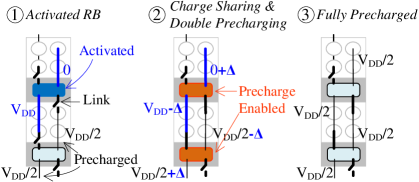
To evaluate the accelerated precharge process, we use the same methodology described in Section 4.3.3 and simulate the linked precharge operation in SPICE. Figure 4.10 shows the resulting timing diagram. During the first 2ns, the wordline is lowered to disconnect the cells from the bitlines . Then, we enable the links to begin precharging the bitlines . The result shows that the precharge latency reduces significantly due to having two PUs to perform the precharge. LISA enables a shorter precharge latency of approximately 3.5ns versus the baseline precharge latency of 13.1ns .
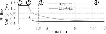
To account for process and temperature variation, we add a guardband to the SPICE-reported latency, increasing it to 5ns (i.e., by 42.9%), which still achieves 2.6x lower precharge latency than the baseline. Our evaluation shows that LISA-LIP improves performance by 10.3% on average, across 50 four-core workloads (see Section 4.9.3).
4.7 Hardware Cost
4.7.1 Die Area Overhead
To evaluate the area overhead of adding isolation transistors, we use area values from prior work, which adds isolation transistors to disconnect bitlines from sense amplifiers [265]. That work shows that adding an isolation transistor to every bitline incurs a total of 0.8% die area overhead in a 28nm DRAM process technology. Similar to prior work that adds isolation transistors to DRAM [193, 265], our LISA substrate also requires additional control logic outside the DRAM banks to control the isolation transistors, which incurs a small amount of area and is non-intrusive to the cell arrays. For LISA-VILLA, we use 1024 six-bit saturating counters to track the access frequency of rows in every bank; this requires an additional 6KB storage within a memory controller connected to one rank.
4.7.2 Handling Repaired Rows
To improve yield, DRAM manufacturers often employ post-manufacturing repair techniques that can remap faulty rows to spare rows provisioned in every subarray [158]. Therefore, consecutive row addresses as observed by the memory controller may physically reside in different subarrays. To handle this issue for techniques that require the controller to know the subarray a row resides in (e.g., RowClone [307], LISA-RISC), a simple approach can be used to expose the repaired row information to the memory controller. Since DRAM already stores faulty rows’ remapping information inside the chip, this information can be exposed to the controller through the serial presence detect (SPD) [136], which is an EEPROM that stores DRAM information such as timing parameters. The memory controller can read this stored information at system boot time so that it can correctly determine a repaired row’s location in DRAM. Note that similar techniques may be necessary for other mechanisms that require information about physical location of rows in DRAM (e.g., [58, 155, 168, 172, 193, 210]).
4.8 Methodology
We evaluate our system using a variant of Ramulator [173], an open-source cycle-accurate DRAM simulator, driven by traces generated from Pin [215]. We will make our simulator publicly available [65]. We use a row buffer policy that closes a row only when there are no more outstanding requests in the memory controller to the same row [293]. Unless stated otherwise, our simulator uses the parameters listed in Table 7.2.
| Processor | 1–4 OoO cores, 4GHz, 3-wide issue |
|---|---|
| Cache | L1: 64KB, L2: 512KB per core, L3: 4MB, 64B lines |
| Mem. Controller | 64/64-entry read/write queue, FR-FCFS [293, 382] |
| DRAM | DDR3-1600 [234], 1–2 channels, 1 rank/channel, |
| 8 banks/rank, 16 subarrays/bank |
To evaluate the benefits of different data copy mechanisms in isolation, we use a copy-aware page mapping policy that allocates destination pages to the same DRAM structures (i.e., subarrays, banks) where the source pages are allocated. As a result, our evaluation of different data copy mechanisms is a limit study as only the specified copy mechanism (e.g., RISC) is used for copy operations. For example, when evaluating RISC, the page mapper allocates both the source and destination pages within the same bank to evaluate the benefits of RISC’s fast data movement between subarrays.
Benchmarks and Workloads. We primarily use benchmarks from TPC(-C/-H) [348], DynoGraph (BFS, PageRank) [281], SPEC CPU2006 [324], and STREAM [225], along with a random-access microbenchmark similar to HPCC RandomAccess [114]. Because these benchmarks predominantly stress the CPU and memory while rarely invoking memcpy, we use the following benchmarks to evaluate different copy mechanisms: (1) bootup, (2) forkbench, and (3) Unix shell. These were shared by the authors of RowClone [307]. The bootup benchmark consists of a trace collected while a Debian operating system was booting up. The forkbench kernel forks a child process that copies 1K pages from the parent process by randomly accessing them from a 64MB array. The Unix shell is a script that runs find in a directory along with ls on each subdirectory. More information on these is in [307].
To construct multi-core workloads for evaluating the benefits of data copy mechanisms, we randomly assemble 50 workloads, each comprising 50% copy-intensive benchmarks and 50% non-copy-intensive benchmarks. To evaluate the benefits of in-DRAM caching and reduced precharge time, we restrict our workloads to randomly-selected memory-intensive ( 5 misses per thousand instructions) non-copy-intensive benchmarks. Due to the large number of workloads, we present detailed results for only five workload mixes (Table 4.3), along with the average results across all 50 workloads.
| Mix 1 | tpcc64, forkbench, libquantum, bootup |
| Mix 2 | bootup, xalancbmk, pagerank, forkbench |
| Mix 3 | libquantum, pagerank, forkbench, bootup |
| Mix 4 | mcf, forkbench, random, forkbench |
| Mix 5 | bfs, bootup, tpch2, bootup |
Performance Metrics. We measure single-core and multi-core performance using IPC and Weighted Speedup (WS) [319], respectively. Prior work showed that WS is a measure of system throughput [86]. To report DRAM energy consumption, we use the Micron power calculator [230]. We run all workloads for 100 million instructions, as done in many recent works [171, 172, 193, 194, 248].
VILLA-DRAM Configuration. For our simulated VILLA-DRAM, each fast subarray consists of 32 rows to achieve low latency on sensing, precharge, and restoration (a typical subarray has 512 rows). Our SPICE simulation reports the following new timing parameters for a 32-row subarray: tRCD=7.5ns, tRP=8.5ns, and tRAS=13ns, which are reduced from the original timings by respectively, 45.5%, 38.2%, and 62.9%. For each bank, we allocate 4 fast subarrays in addition to the 16 512-row subarrays, incurring a 1.6% area overhead. We set the epoch length for our caching policy to 10,000 cycles.
4.9 Evaluation
We quantitatively evaluate our proposed applications of LISA: (1) rapid bulk copying (LISA-RISC), (2) in-DRAM caching with heterogeneous subarrays (LISA-VILLA), and (3) reduced precharge time (LISA-LIP).
4.9.1 Bulk Memory Copy
Single-Core Workloads
Figure 4.11 shows the performance of three copy benchmarks on a single-core system with one memory channel and 1MB of last-level cache (LLC). We evaluate the following bulk copy mechanisms: (1) memcpy, which copies data over the memory channel; (2) RowClone [307]; and (3) LISA-RISC. We use two different hop counts between the source and destination subarray for LISA-RISC: 15 (longest) and 1 (shortest). They are labeled as LISA-RISC-15 and LISA-RISC-1, respectively, in the figure. We make four major observations.
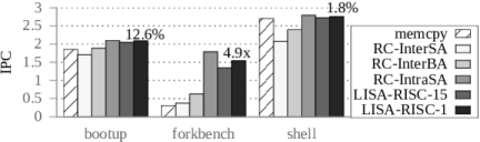
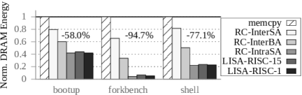
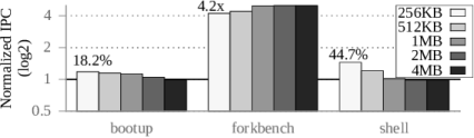
First, LISA-RISC achieves significant improvement over RC-InterSA for all three benchmarks in terms of both IPC and memory energy consumption, shown in Figure 4.11(a) and Figure 4.11(b), respectively. This shows that the LISA substrate is effective at performing fast inter-subarray copies.
Second, both LISA-RISC-1 and LISA-RISC-15 significantly reduce the memory energy consumption over memcpy. This is due to (1) reduced memory traffic over the channel by keeping the data within DRAM, and (2) higher performance.
Third, LISA-RISC-1/-15 provides 12.6%/10.6%, 4.9x/4.3x, and 1.8%/0.7% speedup for bootup, forkbench, and shell, respectively, over memcpy. The performance gains are smaller for bootup and shell. Both of these benchmarks invoke fewer copy operations (i.e., 2171 and 2682, respectively) than forkbench, which invokes a large number (40952) of copies. As a result, forkbench is more sensitive to the memory latency of copy commands. Furthermore, the large LLC capacity (1MB) helps absorb the majority of memory writes resulting from memcpy for bootup and shell, thereby reducing the effective latency of memcpy.
Fourth, RC-InterSA performs worse than memcpy for bootup and shell due to its long blocking copy operations. Although, it attains a 19.4% improvement on forkbench because memcpy causes severe cache pollution by installing a large amount of copied data into the LLC. Compared to the 20% cache hit rate for memcpy, RC-InterSA has a much higher hit rate of 67.2% for forkbench. The copy performance of memcpy is strongly correlated with the LLC management policy and size.
To understand performance sensitivity to LLC size, Figure 4.11(c) shows the speedup of LISA-RISC-1 over memcpy for different LLC capacities. We make two observations, which are also similar for LISA-RISC-15 (not shown). First, for bootup and shell, the speedup of LISA over memcpy reduces as the LLC size increases because the destination locations of memcpy operations are more likely to hit in the larger cache.
Second, for forkbench, LISA-RISC’s performance gain over memcpy decreases as cache size reduces from 1MB to 256KB. This is because the LLC hit rate reduces much more significantly for LISA-RISC, from 67% (1MB) to 10% (256KB), than for memcpy (from 20% at 1MB, to 19% at 256KB). When forkbench uses LISA-RISC for copying data, its working set mainly consists of non-copy data, which has good locality. As the LLC size reduces by 4x, the working set no longer fits in the smaller cache, thus causing a significant hit rate reduction. On the other hand, when memcpy is used as the copy mechanism, the working set of forkbench is mainly from bulk copy data, and is less susceptible to cache size reduction. Nonetheless, LISA-RISC still provides an improvement of 4.2x even with a 256KB cache.
We conclude that LISA-RISC significantly improves performance and memory energy efficiency in single-core workloads that invoke bulk copies.
Multi-Core Workloads
Figure 4.12 shows the system performance and energy efficiency (i.e., memory energy per instruction) of different copy mechanisms across 50 workloads, on a quad-core system with two channels and 4MB of LLC. The error bars in this figure (and other figures) indicate the 25th and 75th percentile values across all 50 workloads. Similar to the performance trends seen in the single-core system, LISA-RISC consistently outperforms other mechanisms at copying data between subarrays. LISA-RISC-1 attains a high average system performance improvement of 66.2% and 2.2x over memcpy and RC-InterSA, respectively. Although Mix 5 has the smallest number of copy operations out of the five presented workload mixes, LISA-RISC still improves its performance by 6.7% over memcpy. By moving copied data only within DRAM, LISA-RISC significantly reduces memory energy consumption (55.4% on average) over memcpy. In summary, LISA-RISC provides both high performance and high memory energy efficiency for bulk data copying for a wide variety of single- and multi-core workloads.
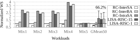
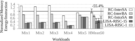
4.9.2 In-DRAM Caching with LISA-VILLA
Figure 4.13 shows the system performance improvement of LISA-VILLA over a baseline without any fast subarrays in a four-core system. It also shows the hit rate in VILLA-DRAM, i.e., the fraction of accesses that hit in the fast subarrays. We make two main observations. First, by exploiting LISA-RISC to quickly cache data in VILLA-DRAM, LISA-VILLA improves system performance for a wide variety of workloads — by up to 16.1%, with a geometric mean of 5.1%. This is mainly due to reduced DRAM latency of accesses that hit in the fast subarrays (which comprise 16MB of total storage across two memory channels). The performance improvement heavily correlates with the VILLA cache hit rate. Our work does not focus on optimizing the caching scheme, but the hit rate may be increased by an enhanced caching policy (e.g., [285, 305]), which can further improve system performance.
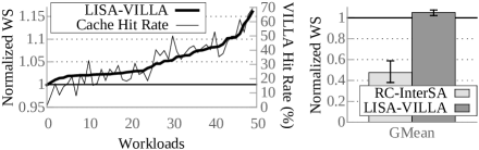
Second, the VILLA-DRAM design, which consists of heterogeneous subarrays, is not practical without LISA. Figure 4.13 shows that using RC-InterSA to move data into the cache reduces performance by 52.3% due to slow data movement, which overshadows the benefits of caching. The results indicate that LISA is an important substrate to enable not only fast bulk data copy, but also a fast in-DRAM caching scheme.
4.9.3 Accelerated Precharge with LISA-LIP
Figure 4.14 shows the system performance improvement of LISA-LIP over a baseline that uses the standard DRAM precharge latency, as well as LISA-LIP’s row-buffer hit rate, on a four-core system across 50 workloads. LISA-LIP attains a maximum gain of 13.2%, with a mean improvement of 8.1%. The performance gain becomes higher as the row-buffer hit rate decreases, which leads to more precharge commands. These results show that LISA is a versatile substrate that effectively reduces precharge latency in addition to accelerating data movement.
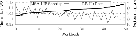
We also evaluate the effectiveness of combining LISA-VILLA and LISA-LIP (not shown, but available in our technical report [59]). The combined mechanism, which is transparent to software, improves system performance by 12.2% on average and up to 23.8% across the same set of 50 workloads without bulk copies. Thus, LISA is an effective substrate that can enable mechanisms to fundamentally reduce memory latency.
4.9.4 Putting Everything Together
As all of the three proposed applications are complementary to each other, we evaluate the effect of putting them together on a four-core system. Figure 4.15 shows the system performance improvement of adding LISA-VILLA to LISA-RISC (15 hops), as well as combining all three optimizations, compared to our baseline using memcpy and standard DDR3-1600 memory. We draw several key conclusions. First, the performance benefits from each scheme are additive. On average, adding LISA-VILLA improves performance by 16.5% over LISA-RISC alone, and adding LISA-LIP further provides an 8.8% gain over LISA-(RISC+VILLA). Second, although LISA-RISC alone provides a majority of the performance improvement over the baseline (59.6% on average), the use of both LISA-VILLA and LISA-LIP further improves performance, resulting in an average performance gain of 94.8% and memory energy reduction (not plotted) of 49.0%. Taken together, these results indicate that LISA is an effective substrate that enables a wide range of high-performance and energy-efficient applications in the DRAM system.
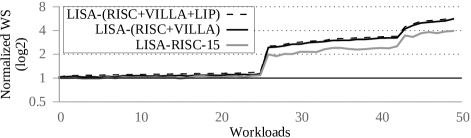
4.9.5 Sensitivity to System Configuration
Figure 4.16 shows the weighted speedup for memcpy and LISA-All (i.e., all three applications) on a 4-core system using varying memory channel counts and LLC sizes. The results show that performance improvement increases with fewer memory channels, as memory contention increases. On the other hand, adding more memory channels increases memory-level parallelism, allowing more of the copy latency to be hidden. Similar trends are observed with the LLC capacity. As LLC size decreases, the working set becomes less likely to fit with memcpy, worsening its performance. LISA-All provides significant performance benefits for all configurations.
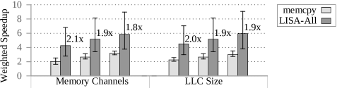
4.9.6 Effect of Copy Distance on LISA-RISC
Table 4.4 shows that the performance gain and memory energy savings of LISA-RISC over memcpy increases as the copy distance reduces. This is because with fewer subarrays between the source and destination subarrays, the number of RBM commands invoked by LISA-RISC reduces accordingly, which decreases the latency and memory energy consumption of bulk data copy.
| Copy Distance (hops) | 1 | 3 | 7 | 15 | 31 | 63 |
|---|---|---|---|---|---|---|
| RISC Copy Latency (ns) | 148.5 | 164.5 | 196.5 | 260.5 | 388.5 | 644.5 |
| WS Improvement (%) | 66.2 | 65.3 | 63.3 | 59.6 | 53.0 | 42.4 |
| DRAM Energy Savings (%) | 55.4 | 55.2 | 54.6 | 53.6 | 51.9 | 48.9 |
4.10 Other Applications Enabled by LISA
We describe two additional applications that can potentially benefit from LISA. We describe them at a high level, and defer evaluations to future work.
Reducing Subarray Conflicts via Remapping. When two memory requests access two different rows in the same bank, they have to be served serially, even if they are to different subarrays. To mitigate such bank conflicts, Kim et al. [172] propose subarray-level parallelism (SALP), which enables multiple subarrays to remain activated at the same time. However, if two accesses are to the same subarray, they still have to be served serially. This problem is exacerbated when frequently-accessed rows reside in the same subarray. To help alleviate such subarray conflicts, LISA can enable a simple mechanism that efficiently remaps or moves the conflicting rows to different subarrays by exploiting fast RBM operations.
Extending the Range of In-DRAM Bulk Operations. To accelerate bitwise operations, Seshadri et al. [306] propose a new mechanism that performs bulk bitwise AND and OR operations in DRAM. Their mechanism is restricted to applying bitwise operations only on rows within the same subarray as it requires the copying of source rows before performing the bitwise operation. The high cost of inter-subarray copies makes the benefit of this mechanism inapplicable to data residing in rows in different subarrays. LISA can enable efficient inter-subarray bitwise operations by using LISA-RISC to copy rows to the same subarray at low latency and low energy.
4.11 Summary
We present a new DRAM substrate, low-cost inter-linked subarrays (LISA), that expedites bulk data movement across subarrays in DRAM. LISA achieves this by creating a new high-bandwidth datapath at low cost between subarrays, via the insertion of a small number of isolation transistors. We describe and evaluate three applications that are enabled by LISA. First, LISA significantly reduces the latency and memory energy consumption of bulk copy operations between subarrays over two state-of-the-art mechanisms [307]. Second, LISA enables an effective in-DRAM caching scheme on a new heterogeneous DRAM organization, which uses fast subarrays for caching hot data in every bank. Third, we reduce precharge latency by connecting two precharge units of adjacent subarrays together using LISA. We experimentally show that the three applications of LISA greatly improve system performance and memory energy efficiency when used individually or together, across a variety of workloads and system configurations.
We conclude that LISA is an effective substrate that enables several effective applications. We believe that this substrate, which enables low-cost interconnections between DRAM subarrays, can pave the way for other applications that can further improve system performance and energy efficiency through fast data movement in DRAM.
Chapter 5 Mitigating Refresh Latency by Parallelizing Accesses with Refreshes
In the previous chapter, we describe LISA, a new DRAM substrate, that significantly reduces inter-subarray movement latency to enable several low-latency optimizations. While LISA primarily targets the latency incurred on demand requests issued from the applications, it does not address the latency problem due to a DRAM maintenance operation, refresh, which is issued periodically by the memory controllers to recharge the cells’ data.
Each DRAM cell must be refreshed periodically every refresh interval as specified by the DRAM standards [135, 138]. The exact refresh interval time depends on the DRAM type (e.g., DDR or LPDDR) and the operating temperature. While DRAM is being refreshed, it becomes unavailable to serve memory requests. As a result, refresh latency significantly degrades system performance [211, 241, 254, 327] by delaying in-flight memory requests. This problem will become more prevalent as DRAM density increases, leading to more DRAM rows to be refreshed within the same refresh interval. DRAM chip density is expected to increase from 8Gb to 32Gb by 2020 as it doubles every two to three years [130]. Our evaluations show that DRAM refresh, as it is performed today, causes an average performance degradation of 8.2% and 19.9% for 8Gb and 32Gb DRAM chips, respectively, on a variety of memory-intensive workloads running on an 8-core system. Hence, it is important to develop practical mechanisms to mitigate the performance penalty of DRAM refresh. In this chapter, we propose two complementary mechanisms to mitigate the negative performance impact of refresh: DARP (Dynamic Access Refresh Parallelization) and SARP (Subarray Access Refresh Parallelization) The goal is to address the draw- backs of per-bank refresh by building more efficient techniques to parallelize refreshes and accesses within DRAM.
5.1 Motivation
In this section, we first describe the scaling trend of commonly used all-bank refresh in both LPDDR and DDR DRAM as chip density increases in the future. We then provide a quantitative analysis of all-bank refresh to show its performance impact on multi-core systems followed by performance comparisons to per-bank refresh that is only supported in LPDDR.
5.1.1 Increasing Performance Impact of Refresh
During the time period, the entire memory rank is locked up, preventing the memory controller from sending any memory request. As a result, refresh operations degrade system performance by increasing the latency of memory accesses. The negative impact on system performance is expected to be exacerbated as increases with higher DRAM density. The value of is currently 350ns for an 8Gb memory device [135]. Figure 5.1 shows our estimated trend of for future DRAM generations using linear extrapolation on the currently available and previous DRAM devices. The same methodology is used in prior works [211, 327]. Projection 1 is an extrapolation based on 1, 2, and 4Gb devices; Projection 2 is based on 4 and 8Gb devices. We use the more optimistic Projection 2 for our evaluations. As it shows, may reach up to 1.6s for future 64Gb DRAM devices. This long period of unavailability to process memory accesses is detrimental to system performance.
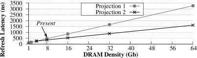
To demonstrate the negative system performance impact of DRAM refresh, we evaluate 100 randomly mixed workloads categorized to five different groups based on memory intensity on an 8-core system using various DRAM densities.111Detailed methodology is described in Section 5.3, including workloads, simulation methodology, and performance metrics. We use up to 32Gb DRAM density that the ITRS predicts to be manufactured by 2020 [130]. Figure 5.2 shows the average performance loss due to all-bank refresh compared to an ideal baseline without any refreshes for each memory-intensity category. The performance degradation due to refresh becomes more severe as either DRAM chip density (i.e., ) or workload memory intensity increases (both of which are trends in systems), demonstrating that it is increasingly important to address the problem of DRAM refresh.
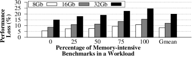
Even though the current DDR3 standard does not support , we believe that it is important to evaluate the performance impact of on DDR3 DRAM because DDR3 DRAM chips are widely deployed in desktops and servers. Furthermore, adding per-bank refresh support to a DDR3 DRAM chip should be non-intrusive because it does not change the internal bank organization. We estimate the refresh latency of in a DDR3 chip based on the values used in an LPDDR2 chip. In a 2Gb LPDDR2 chip, the per-bank refresh latency () is 90ns and the all-bank refresh latency () is 210ns, which takes 2.3x longer than [231].222LPDDR2 has a shorter than DDR3 because LPDDR2 1) has a retention time of 32ms instead of 64ms in DDR3 under normal operating temperature and 2) each operation refreshes fewer rows. We apply this multiplicative factor to to calculate .
Based on the estimated values, we evaluate the performance impact of on the same 8-core system and workloads.1 Figure 5.3 shows the average performance degradation of and compared to an ideal baseline without any refreshes. Even though provides performance gains over by allowing DRAM accesses to non-refreshing banks, its performance degradation becomes exacerbated as increases with higher DRAM density. With 32Gb DRAM chips using , the performance loss due to DRAM refresh is still a significant 16.6% on average, which motivates us to address issues related to .

5.1.2 Our Goal
We identify two main problems that faces. First, commands are scheduled in a very restrictive manner in today’s systems. Memory controllers have to send commands in a sequential round-robin order without any flexibility. Therefore, the current implementation does not exploit the full benefit from overlapping refreshes with accesses across banks. Second, cannot serve accesses to a refreshing bank until the refresh of that bank is complete. Our goal is to provide practical mechanisms to address these two problems so that we can minimize the performance overhead of DRAM refresh.
5.2 Mechanisms
5.2.1 Overview
We propose two mechanisms, Dynamic Access Refresh Parallelization (DARP) and Subarray Access Refresh Parallelization (SARP), that hide refresh latency by parallelizing refreshes with memory accesses across banks and subarrays, respectively. DARP is a new refresh scheduling policy that consists of two components. The first component is out-of-order per-bank refresh that enables the memory controller to specify a particular (idle) bank to be refreshed as opposed to the standard per-bank refresh policy that refreshes banks in a strict round-robin order. With out-of-order refresh scheduling, DARP can avoid refreshing (non-idle) banks with pending memory requests, thereby avoiding the refresh latency for those requests. The second component is write-refresh parallelization that proactively issues per-bank refresh to a bank while DRAM is draining write batches to other banks, thereby overlapping refresh latency with write latency. The second mechanism, SARP, allows a bank to serve memory accesses in idle subarrays while other subarrays within the same bank are being refreshed. SARP exploits the fact that refreshing a row is contained within a subarray, without affecting the other subarrays’ components and the I/O bus used for transferring data. We now describe each mechanism in detail.
5.2.2 Dynamic Access Refresh Parallelization
Out-of-order Per-bank Refresh
The limitation of the current per-bank refresh mechanism is that it disallows a memory controller from specifying which bank to refresh. Instead, a DRAM chip has internal logic that strictly refreshes banks in a sequential round-robin order. Because DRAM lacks visibility into a memory controller’s state (e.g., request queues’ occupancy), simply using an in-order policy can unnecessarily refresh a bank that has multiple pending memory requests to be served when other banks may be free to serve a refresh command. To address this problem, we propose the first component of DARP, out-of-order per-bank refresh. The idea is to remove the bank selection logic from DRAM and make it the memory controller’s responsibility to determine which bank to refresh. As a result, the memory controller can refresh an idle bank to enhance parallelization of refreshes and accesses, avoiding refreshing a bank that has pending memory requests as much as possible.
Due to reordering, the memory controller needs to guarantee that deviating from the original in-order schedule still preserves data integrity. To achieve this, we take advantage of the fact that the contemporary DDR JEDEC standard [135, 137] actually provides some refresh scheduling flexibility. The standard allows up to eight all-bank refresh commands to be issued late (postponed) or early (pulled-in). This implies that each bank can tolerate up to eight to be postponed or pulled-in. Therefore, the memory controller ensures that reordering preserves data integrity by limiting the number of postponed or pulled-in commands.
Figure 5.4 shows the algorithm of our mechanism. The out-of-order per-bank refresh scheduler makes a refresh decision every DRAM cycle. There are three key steps. First, when the memory controller hits a per-bank refresh schedule time (every ), it postpones the scheduled if the to-be-refreshed bank (R) has pending demand requests (read or write) and it has postponed fewer refreshes than the limit of eight ( ). The hardware counter that is used to keep track of whether or not a refresh can be postponed for each bank is called the refresh credit (ref_credit). The counter decrements on a postponed refresh and increments on a pulled-in refresh for each bank. Therefore, a command can be postponed if the bank’s ref_credit stays between values of 0 and 8 (). Otherwise the memory controller is required to send a command when more than eight commands have been postponed (i.e., ) to comply with the standard. Each resets the bank’s ref_credit value bank to 0. Second, the memory controller prioritizes issuing commands for a demand request if a refresh is not sent at any given time ( ). Third, if the memory controller cannot issue any commands for demand requests due to the timing constraints, it instead randomly selects one bank (B) from a list of banks that have no pending demand requests to refresh. Such a refresh command is either a previously postponed or a new pulled-in ( ).
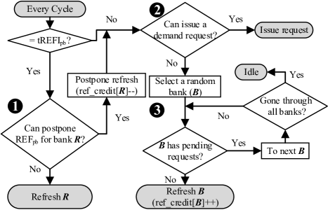
Write-refresh Parallelization
The key idea of the second component of DARP is to actively avoid refresh interference on read requests and instead enable more parallelization of refreshes with write requests. We make two observations that lead to our idea. First, write batching in DRAM creates an opportunity to overlap a refresh operation with a sequence of writes, without interfering with reads. A modern memory controller typically buffers DRAM writes and drains them to DRAM in a batch to amortize the bus turnaround latency, also called tWTR or tRTW [135, 172, 186], which is the additional latency incurred from switching between serving writes to reads because DRAM I/O bus is half-duplex. Typical systems start draining writes when the write buffer occupancy exceeds a certain threshold until the buffer reaches a low watermark. This draining time period is called the writeback mode, during which no rank within the draining channel can serve read requests [62, 186, 326]. Second, DRAM writes are not latency-critical because processors do not stall to wait for them: DRAM writes are due to dirty cache line evictions from the last-level cache [186, 326].
Given that writes are not latency-critical and are drained in a batch for some time interval, we propose the second component of DARP, write-refresh parallelization, that attempts to maximize parallelization of refreshes and writes. Write-refresh parallelization selects the bank with the minimum number of pending demand requests (both read and write) and preempts the bank’s writes with a per-bank refresh. As a result, the bank’s refresh operation is hidden by the writes in other banks.
The reasons why we select the bank with the lowest number of demand requests as a refresh candidate during writeback mode are two-fold. First, the goal of the writeback mode is to drain writes as fast as possible to reach a low watermark that determines the end of the writeback mode [62, 186, 326]. Extra time delay on writes can potentially elongate the writeback mode by increasing queueing delay and reducing the number of writes served in parallel across banks. Refreshing the bank with the lowest write request count (zero or more) has the smallest impact on the writeback mode length because other banks can continue serving their writes to reach to the low watermark. Second, if the refresh scheduled to a bank during the writeback mode happens to extend beyond writeback mode, it is likely that the refresh 1) does not delay immediate reads within the same bank because the selected bank has no reads or 2) delays reads in a bank that has less contention. Note that we only preempt one bank for refresh because the JEDEC standard [138] disallows overlapping per-bank refresh operations across banks within a rank.
Figure 5.5 shows the service timeline and benefits of write-refresh parallelization. There are two scenarios when the scheduling policy parallelizes refreshes with writes to increase DRAM’s availability to serve read requests. Figure 5.5(a) shows the first scenario when the scheduler postpones issuing a command to avoid delaying a read request in Bank 0 and instead serves the refresh in parallel with writes from Bank 1, effectively hiding the refresh latency in the writeback mode. Even though the refresh can potentially delay individual write requests during writeback mode, the delay does not impact performance as long as the length of writeback mode remains the same as in the baseline due to longer prioritized write request streams in other banks. In the second scenario shown in Figure 5.5(b), the scheduler proactively pulls in a command early in Bank 0 to fully hide the refresh latency from the later read request while Bank 1 is draining writes during the writeback mode (note that the read request cannot be scheduled during the writeback mode).
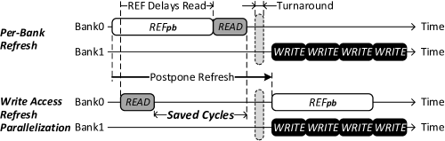
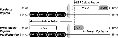
The crucial observation is that write-refresh parallelization improves performance because it avoids stalling the read requests due to refreshes by postponing or pulling in refreshes in parallel with writes without extending the writeback period.
Algorithm 1 shows the operation of write-refresh parallelization. When the memory controller enters the writeback mode, the scheduler selects a bank candidate for refresh when there is no pending refresh. A bank is selected for refresh under the following criteria: 1) the bank has the lowest number of demand requests among all banks and 2) its refresh credit has not exceeded the maximum pulled-in refresh threshold. After a bank is selected for refresh, its credit increments by one to allow an additional refresh postponement.
Every in Writeback Mode:
Implementation
DARP incurs a small overhead in the memory controller and DRAM without affecting the DRAM cell array organization. There are five main modifications. First, each refresh credit is implemented with a hardware integer counter that either increments or decrements by up to eight when a refresh command is pulled-in or postponed, respectively. Thus, the storage overhead is very modest with 4 bits per bank (32 bits per rank). Second, DARP requires logic to monitor the status of various existing queues and schedule refreshes as described. Despite reordering refresh commands, all DRAM timing constraints are followed, notably tRRD and that limit when can be issued to DRAM. Third, the DRAM command decoder needs modification to decode the bank ID that is sent on the address bus with the command. Fourth, the refresh logic that is located outside of the banks and arrays needs to be modified to take in the specified bank ID. Fifth, each bank requires a separate row counter to keep track of which rows to refresh as the number of postponed or pulled-in refresh commands differs across banks. Our proposal limits the modification to the least invasive part of the DRAM without changing the structure of the dense arrays that consume the majority of the chip area.
5.2.3 Subarray Access Refresh Parallelization
Even though DARP allows refreshes and accesses to occur in parallel across different banks, DARP cannot deal with their collision within a bank. To tackle this problem, we propose SARP (Subarray Access Refresh Parallelization) that exploits the existence of subarrays within a bank. The key observation leading to our second mechanism is that refresh occupies only a few subarrays within a bank whereas the other subarrays and the I/O bus remain idle during the process of refreshing. The reasons for this are two-fold. First, refreshing a row requires only its subarray’s sense amplifiers that restore the charge in the row without transferring any data through the I/O bus. Second, each subarray has its own set of sense amplifiers that are not shared with other subarrays.
Based on this observation, SARP’s key idea is to allow memory accesses to an idle subarray while another subarray is refreshing. Figure 5.6 shows the service timeline and the performance benefit of our mechanism. As shown, SARP reduces the read latency by performing the read operation to Subarray 1 in parallel with the refresh in Subarray 0. Compared to DARP, SARP provides the following advantages: 1) SARP is applicable to both all-bank and per-bank refresh, 2) SARP enables memory accesses to a refreshing bank, which cannot be achieved with DARP, and 3) SARP also utilizes bank-level parallelism by serving memory requests from multiple banks while the entire rank is under refresh. SARP requires modifications to 1) the DRAM architecture because two distinct wordlines in different subarrays need to be raised simultaneously, which cannot be done in today’s DRAM due to the shared peripheral logic among subarrays, 2) the memory controller such that it can keep track of which subarray is under refresh in order to send the appropriate memory request to an idle subarray.
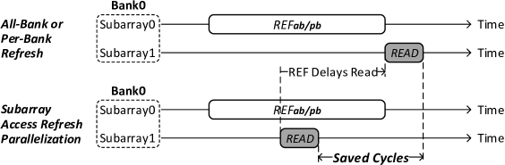
DRAM Bank Implementation for SARP
As opposed to DARP, SARP requires modifications to DRAM to support accessing subarrays individually. While subarrays are equipped with dedicated local peripheral logic, what prevents the subarrays from being operated independently is the global peripheral logic that is shared by all subarrays within a bank.
Figure 5.7(a) shows a detailed view of an existing DRAM bank’s organization. There are two major shared peripheral components within a bank that prevent modern DRAM chips to refresh at subarray level. First, each bank has a global row decoder that decodes the incoming row’s addresses. To read or write a row, memory controllers first issue an activate command with the row’s address. Upon receiving this command, the bank feeds the row address to the global row decoder that broadcasts the partially decoded address to all subarrays within the bank. After further decoding, the row’s subarray then raises its wordline to begin transferring the row’s cells’ content to the row buffer.333The detailed step-to-step explanation of the activation process can be found in prior works [172, 193, 307]. During the transfer, the row buffer also restores the charge in the row. Similar to an activate, refreshing a row requires the refresh unit to activate the row to restore its electrical charge (only the refresh row counter is shown for clarity in Figure 5.7(a)). Because a bank has only one global row decoder and one pair of address wires (for subarray row address and ID), it cannot simultaneously activate two different rows (one for a memory access and the other for a refresh).
Second, when the memory controller sends a read or write command, the required column from the activated row is routed through the global bitlines into the global I/O buffer (both of which are shared across all subarrays’ row buffers) and is transferred to the I/O bus. This is done by asserting a column select signal that is routed globally to all subarrays, which enables all subarrays’ row buffers to be concurrently connected to the global bitlines. Since this signal connects all subarrays’ row buffers to the global bitlines at the same time, if more than one activated row buffer (i.e., activated subarray) exists in the bank, an electrical short-circuit occurs, leading to incorrect operation. As a result, two subarrays cannot be kept activated when one is being read or written to, which prevents a refresh to one subarray from happening concurrently with an access in a different subarray in today’s DRAM.
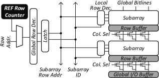
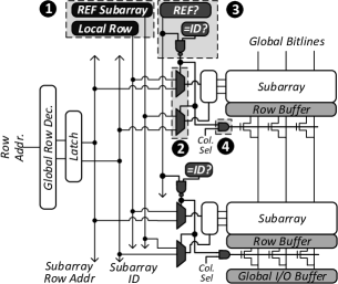
The key idea of SARP is to allow the concurrent activation of multiple subarrays, but to only connect the accessed subarray’s row buffer to the global bitlines while another subarray is refreshing. Figure 5.7(b) shows our proposed changes to the DRAM microarchitecture. There are two major enablers of SARP.
The first enabler of SARP allows both refresh and access commands to simultaneously select their designated rows and subarrays with three new components. The first component ( ) provides the subarray and row addresses for refreshes without relying on the global row decoder. To achieve this, it decouples the refresh row counter into a refresh-subarray counter and a local-row counter that keep track of the currently refreshing subarray and the row address within that subarray, respectively. The second component ( ) allows each subarray to activate a row for either a refresh or an access through two muxes. One mux is a row-address selector and the other one is a subarray selector. The third component ( ) serves as a control unit that chooses a subarray for refresh. The REF? block indicates if the bank is currently under refresh and the =ID? comparator determines if the corresponding subarray’s ID matches with the refreshing subarray counter for refresh. These three components form a new address path for the refresh unit to supply refresh addresses in parallel with addresses for memory accesses.
The second enabler of SARP allows accesses to one activated subarray while another subarray is kept activated for refreshes. We add an AND gate ( ) to each subarray that ensures the refreshing subarray’s row buffer is not connected to the global bitlines when the column select signal is asserted on an access. At any instance, there is at most one activated subarray among all non-refreshing subarrays because the global row decoder activates only one subarray at a time. With the two proposed enablers, SARP allows one activated subarray for refreshes in parallel with another activated subarray that serves data to the global bitlines.
Detecting Subarray Conflicts in the Memory Controller
To avoid accessing a refreshing subarray, which is determined internally by the DRAM chip in our current mechanism, the memory controller needs to know the current refreshing subarray and the number of subarrays. We create shadow copies of the refresh-subarray and local-row counters in the memory controller to keep track of the currently-refreshing subarray. We store the number of subarrays in an EEPROM called the serial presence detect (SPD) [136], which stores various timing and DRAM organization information in existing DRAM modules. The memory controller reads this information at system boot time so that it can issue commands correctly.444Note that it is possible to extend our mechanisms such that the memory controller specifies the subarray to be refreshed instead of the DRAM chip. This requires changes to the DRAM interface.
Power Integrity
Because an activate draws a lot of current, DRAM standards define two timing parameters to constrain the activity rate of DRAM so that activates do not over-stress the power delivery network [135, 314]. The first parameter is the row-to-row activation delay (tRRD) that specifies the minimum waiting time between two subsequent activate commands within a DRAM device. The second is called the four activate window (tFAW) that defines the length of a rolling window during which a maximum of four activates can be in progress. Because a refresh operation requires activating rows to restore charge in DRAM cells, SARP consumes additional power by allowing accesses during refresh. To limit the power consumption due to activates, we further constrain the activity rate by increasing both tFAW and tRRD, as shown below. This results in fewer activate commands issued during refresh.
| (5.1) | ||||
| (5.2) | ||||
| (5.3) |
and represent the current values of an activate and a refresh, respectively, based on the Micron Power Calculator [230]. We calculate the power overhead of parallelizing a refresh over a four activate window using (5.1). Then we apply this power overhead to both tFAW (5.2) and tRRD (5.3), which are enforced during refresh operations. Based on the values in the Micron 8Gb DRAM [232] data sheet, SARP increases tFAW and tRRD by 2.1x during all-bank refresh operations. Each per-bank refresh consumes 8x lower current than an all-bank refresh, thus increasing tFAW and tRRD by only 13.8%.
Die Area Overhead
In our evaluations, we use 8 subarrays per bank and 8 banks per DRAM chip. Based on this configuration, we calculate the area overhead of SARP using parameters from a Rambus DRAM model at 55 technology [291], the best publicly available model that we know of, and find it to be 0.71% in a 2Gb DDR3 DRAM chip with a die area of 73.5. The power overhead of the additional components is negligible compared to the entire DRAM chip.
5.3 Methodology
To evaluate our mechanisms, we use an in-house cycle-level x86 multi-core simulator with a front end driven by Pin [215] and an in-house cycle-accurate DRAM timing model validated against DRAMSim2 [295]. Unless stated otherwise, our system configuration is as shown in Table 5.1.
| Processor | 8 cores, 4GHz, 3-wide issue, 8 MSHRs/core, |
|---|---|
| 128-entry instruction window | |
| Last-level Cache | 64B cache-line, 16-way associative, |
| 512KB private cache-slice per core | |
| Memory Controller | 64/64-entry read/write request queue, FR-FCFS [293], |
| writes are scheduled in batches [62, 186, 326] with | |
| low watermark = 32, closed-row policy [62, 171, 293] | |
| DRAM | DDR3-1333 [232], 2 channels, 2 ranks per channel, |
| 8 banks/rank, 8 subarrays/bank, 64K rows/bank, 8KB rows | |
| Refresh Settings | = 350/530/890ns for 8/16/32Gb DRAM chips, |
| = 3.9µs, -to- ratio = 2.3 |
In addition to 8Gb DRAM, we also evaluate systems using 16Gb and 32Gb near-future DRAM chips [130]. Because commodity DDR DRAM does not have support for , we estimate the values for DDR3 based on the ratio of to in LPDDR2 [231] as described in Section 5.1.1. We evaluate our systems with 32ms retention time, which is a typical setting for a server environment and LPDDR DRAM, as also evaluated in previous work [254, 327].
We use benchmarks from SPEC CPU2006 [324], STREAM [225], TPC [348], and a microbenchmark with random-access behavior similar to HPCC RandomAccess [114]. We classify each benchmark as either memory intensive (MPKI 10) or memory non-intensive (MPKI 10). We then form five intensity categories based on the fraction of memory intensive benchmarks within a workload: 0%, 25%, 50%, 75%, and 100%. Each category contains 20 randomly mixed workloads, totaling to 100 workloads for our main evaluations. For sensitivity studies in Sections 5.4.1, 5.4.2, 5.4.3, and 5.4.4, we run 16 randomly selected memory-intensive workloads using 32Gb DRAM to observe the performance trend.
We measure system performance with the commonly-used weighted speedup (WS) [86, 319] metric. To report the DRAM system power, we use the methodology from the Micron power calculator [230]. The DRAM device parameters are obtained from [232]. Every workload runs for 256 million cycles to ensure the same number of refreshes. We report DRAM system power as energy per memory access serviced to fairly compare across different workloads.
5.4 Evaluation
In this section, we evaluate the performance of the following mechanisms: 1) the all-bank refresh scheme (), 2) the per-bank refresh scheme (), 3) elastic refresh [327], 4) our first mechanism, DARP, 5) our second mechanism, SARP, that is applied to either () or (), 6) the combination of DARP and , called DSARP, and 7) an ideal scheme that eliminates refresh. Elastic refresh [327] takes advantage of the refresh scheduling flexibility in the DDR standard: it postpones a refresh if the refresh is predicted to interfere with a demand request, based on a prediction of how long a rank will be idle, i.e., without any demand request.
5.4.1 Multi-Core Results
Figure 5.8 plots the system performance improvement of , DARP, , and DSARP over the all-bank refresh baseline () using various densities across 100 workloads (sorted based on the performance improvement due to DARP). The x-axis shows the sorted workload numbers as categorized into five memory-intensive groups with 0 to 19 starting in the least memory-intensive group and 80 to 99 in the most memory-intensive one. Table 5.2 shows the maximum and geometric mean of system performance improvement due to our mechanisms over and for different DRAM densities. We draw five key conclusions from these results.
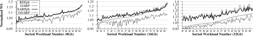
First, DARP provides system performance gains over both and schemes: 2.8%/4.9%/3.8% and 7.4%/9.8%/8.3% on average in 8/16/32Gb DRAMs, respectively. The reason is that DARP hides refresh latency with writes and issues refresh commands in out-of-order fashion to reduce refresh interference on reads. Second, provides significant system performance improvement over DARP and refresh baselines for all the evaluated DRAM densities as enables accesses to idle subarrays in the refreshing banks. ’s average system performance improvement over and is 3.3%/6.7%/13.7% and 7.9%/11.7%/18.6% in 8/16/32Gb DRAMs, respectively. Third, as density increases, the performance benefit of over DARP gets larger. This is because the longer refresh latency becomes more difficult to hide behind writes or idle banks for DARP. This is also the reason why the performance improvement due to DARP drops slightly at 32Gb compared to 16Gb. On the other hand, is able to allow a long-refreshing bank to serve some memory requests in its subarrays.
Fourth, combining both and DARP (DSARP) provides additive system performance improvement by allowing even more parallelization of refreshes and memory accesses. As DRAM density (refresh latency) increases, the benefit becomes more apparent, resulting in improvement up to 27.0% and 36.6% over and in 32Gb DRAM, respectively.
Fifth, performs worse than for some workloads (the curves of dropping below one) and the problem is exacerbated with longer refresh latency. Because commands cannot overlap with each other [138], their latencies are serialized. In contrast, operates on every bank in parallel, which is triggered by a single command that partially overlaps refreshes across different banks [241]. Therefore, in a pathological case, the latency for refreshing every bank (eight in most DRAMs) in a rank is , whereas all-bank refresh takes (see Section 5.1.1). If a workload cannot effectively utilize multiple banks during a per-bank refresh operation, may potentially degrade system performance compared to .
| Density | Mechanism | Max (%) | Gmean (%) | ||
|---|---|---|---|---|---|
| 8Gb | DARP | 6.5 | 17.1 | 2.8 | 7.4 |
| 7.4 | 17.3 | 3.3 | 7.9 | ||
| DSARP | 7.1 | 16.7 | 3.3 | 7.9 | |
| 16Gb | DARP | 11.0 | 23.1 | 4.9 | 9.8 |
| 11.0 | 23.3 | 6.7 | 11.7 | ||
| DSARP | 14.5 | 24.8 | 7.2 | 12.3 | |
| 32Gb | DARP | 10.7 | 20.5 | 3.8 | 8.3 |
| 21.5 | 28.0 | 13.7 | 18.6 | ||
| DSARP | 27.0 | 36.6 | 15.2 | 20.2 | |
All Mechanisms’ Results
Figure 5.9 shows the average performance improvement due to all the evaluated refresh mechanisms over . The weighted speedup value for is 5.5/5.3/4.8 using 8/16/32Gb DRAM density. We draw three major conclusions. First, using SARP on all-bank refresh () also significantly improves system performance. This is because SARP allows a rank to continue serving memory requests while it is refreshing. Second, elastic refresh does not substantially improve performance, with an average of 1.8% over all-bank refresh. This is because elastic refresh does not attempt to pull in refresh opportunistically, nor does it try to overlap refresh latency with other memory accesses. The observation is consistent with prior work [254]. Third, DSARP captures most of the benefit of the ideal baseline (”No REF”), performing within 0.9%, 1.2%, and 3.7% of the ideal for 8, 16, and 32Gb DRAM, respectively.
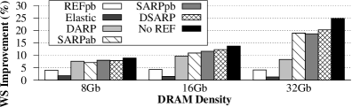
Performance Breakdown of DARP
To understand the observed performance gain in more detail, we evaluate the performance of DARP’s two components separately. Out-of-order per-bank refresh improves performance by 3.2%/3.9%/3.0% on average and up to 16.8%/21.3%/20.2% compared to in 8/16/32Gb DRAMs. Adding write-refresh parallelization to out-of-order per-bank refresh (DARP) provides additional performance gains of 4.3%/5.8%/5.2% on average by hiding refresh latency with write accesses.
Energy
Our techniques reduce energy per memory access compared to existing policies, as shown in Figure 5.10. The main reason is that the performance improvement reduces average static energy for each memory access. Note that these results conservatively assume the same power parameters for 8, 16, and 32 Gb chips, so the savings in energy would likely be more significant if realistic power parameters are used for the more power-hungry 16 and 32 Gb nodes.
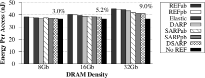
Effect of Memory Intensity
Figure 5.11 shows the performance improvement of DSARP compared to and on workloads categorized by memory intensity (% of memory-intensive benchmarks in a workload), respectively. We observe that DSARP outperforms and consistently. Although the performance improvement of DSARP over increases with higher memory intensity, the gain over begins to plateau when the memory intensity grows beyond 25%. This is because ’s benefit over also increases with memory intensity as enables more accesses to be be parallelized with refreshes. Nonetheless, our mechanism provides the highest system performance compared to prior refresh policies.
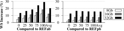
Effect of Core Count
Table 5.3 shows the weighted speedup, harmonic speedup, fairness, and energy-per-access improvement due to DSARP compared to for systems with 2, 4, and 8 cores. For all three systems, DSARP consistently outperforms the baseline without unfairly penalizing any specific application. We conclude that DSARP is an effective mechanism to improve performance, fairness and energy of multi-core systems employing high-density DRAM.
5.4.2 Effect of tFAW
Table 5.4 shows the performance improvement of over when we vary tFAW in DRAM cycles (20 cycles for the baseline as specified by the data sheet) and when tRRD scales proportionally with tFAW.555We evaluate only because it is sensitive to tFAW and tRRD as it extends these parameters during parallelization of refreshes and accesses to compensate for the power overhead. As tFAW reduces, the performance benefit of increases over . This is because reduced tFAW enables more accesses/refreshes to happen in parallel, which our mechanism takes advantage of.
| tFAW/tRRD (DRAM cycles) | 5/1 | 10/2 | 15/3 | 20/4 | 25/5 | 30/6 |
|---|---|---|---|---|---|---|
| WS Improvement (%) | 14.0 | 13.9 | 13.5 | 12.4 | 11.9 | 10.3 |
5.4.3 Effect of Subarrays-Per-Bank
Table 5.5 shows that the average performance gain of over increases as the number of subarrays increases in 32Gb DRAM. This is because with more subarrays, the probability of memory requests to a refreshing subarray reduces.
| Subarrays-per-bank | 1 | 2 | 4 | 8 | 16 | 32 | 64 |
|---|---|---|---|---|---|---|---|
| WS Improvement (%) | 0 | 3.8 | 8.5 | 12.4 | 14.9 | 16.2 | 16.9 |
5.4.4 Effect of Refresh Interval
For our studies so far, we use 32ms retention time (i.e., = 3.9s) that represents a typical setting for a server environment and LPDDR DRAM [138]. Table 5.6 shows the performance improvement of DSARP over two baseline refresh schemes using retention time of 64ms (i.e., = 7.8s). DSARP consistently provides performance gains over both refresh schemes. The maximum performance improvement over is higher than that over at 32Gb because actually degrades performance compared to for some workloads, as discussed in the 32ms results (Section 5.4.1).
| Density | Max (%) | Gmean (%) | ||
|---|---|---|---|---|
| 8Gb | 2.5 | 5.8 | 1.0 | 3.3 |
| 16Gb | 4.6 | 8.6 | 2.6 | 5.3 |
| 32Gb | 18.2 | 13.6 | 8.0 | 9.1 |
5.4.5 DDR4 Fine Granularity Refresh
DDR4 DRAM supports a new refresh mode called fine granularity refresh (FGR) in an attempt to mitigate the increasing refresh latency () [137]. FGR trades off shorter with faster refresh rate () that increases by either 2x or 4x. Figure 5.12 shows the effect of FGR in comparison to , adaptive refresh policy (AR) [241], and DSARP. 2x and 4x FGR actually reduce average system performance by 3.9%/4.0%/4.3% and 8.1%/13.7%/15.1% compared to with 8/16/32Gb densities, respectively. As the refresh rate increases by 2x/4x (higher refresh penalty), does not scale down with the same constant factors. Instead, reduces by 1.35x/1.63x with 2x/4x higher rate [137], thus increasing the worst-case refresh latency by 1.48x/2.45x. This performance degradation due to FGR has also been observed in Mukundan et al. [241]. AR [241] dynamically switches between 1x (i.e., ) and 4x refresh modes to mitigate the downsides of FGR. AR performs slightly worse than (within 1%) for all densities. Because using 4x FGR greatly degrades performance, AR can only mitigate the large loss from the 4x mode and cannot improve performance over . On the other hand, DSARP is a more effective mechanism to tolerate the long refresh latency than both FGR and AR as it overlaps refresh latency with access latency without increasing the refresh rate.
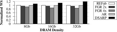
5.5 Summary
We introduced two new complementary techniques, DARP (Dynamic Access Refresh Parallelization) and SARP (Subarray Access Refresh Parallelization), to mitigate the DRAM refresh penalty by enhancing refresh-access parallelization at the bank and subarray levels, respectively. DARP 1) issues per-bank refreshes to idle banks in an out-of-order manner instead of issuing refreshes in a strict round-robin order, 2) proactively schedules per-bank refreshes during intervals when a batch of writes are draining to DRAM. SARP enables a bank to serve requests from idle subarrays in parallel with other subarrays that are being refreshed. Our extensive evaluations on a wide variety of systems and workloads show that these mechanisms significantly improve system performance and outperform state-of-the-art refresh policies, approaching the performance of ideally eliminating all refreshes. We conclude that DARP and SARP are effective in hiding the refresh latency penalty in modern and near-future DRAM systems, and that their benefits increase as DRAM density increases.
Chapter 6 FLY-DRAM: Understanding and Exploiting Latency Variation in DRAM
DRAM standards define a fixed value for each of the timing parameters, which determine the latency of DRAM operations. Unfortunately, these latencies do not reflect the actual time the DRAM operations take for each cell. This is because the true access latency varies for each cell, as every cell is different in size and strength due to manufacturing process variation effects. For simplicity, and to ensure that DRAM yield remains high, DRAM manufacturers define a single set of latencies that guarantees reliable operation, based on the slowest cell in any DRAM chip across all DRAM vendors. As a result, there is a significant opportunity to reduce DRAM latency if, instead of always using worst-case latencies, we employ the true latency for each cell that enables the three operations reliably.
Our goal in this chapter is to (i) understand the impact of cell variation in the three fundamental DRAM operations for cell access (activation, precharge, and restoration); (ii) experimentally characterize the latency variation in these operations; and (iii) develop new mechanisms that take advantage of this variation to reduce the latency of these three operations.
6.1 Motivation
The latencies of the three DRAM operations (activation, precharge, and restoration), as defined by vendor specifications, have not improved significantly in the past 18 years, as depicted in Figure 6.1. This is especially true when we compare latency improvements to the capacity (128=) and bandwidth improvements (20) [135, 137, 193, 320, 192] commodity DRAM chips experienced in the past 18 years. In fact, the activation and precharge latencies increased from 2013 to 2015, when DDR DRAM transitioned from the third generation (12.5ns for DDR3-1600J [135]) to the fourth generation (14.06ns for DDR4-2133P [137]). As the latencies specified by vendors have not reduced over time, the system performance bottleneck caused by raw main memory latency remains largely unaddressed in modern systems.
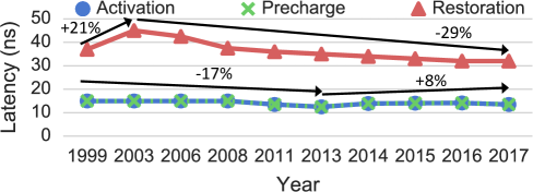
In this chapter, we observe that the three fundamental DRAM operations can actually complete with a much lower latency for many DRAM cells than the specification, because there is inherent latency variation present across the DRAM cells within a DRAM chip. This is a result of manufacturing process variation, which causes the sizes and strengths of cells to be different, thus making some cells inherently faster and other cells inherently slower to be accessed reliably [200]. The speed gap between the fastest and the slowest DRAM cells is getting worse [53, 267], as the technology node continues to scale down to sub-20nm feature sizes. Unfortunately, instead of optimizing the latency specifications for the common case, DRAM vendors use a single set of standard access latencies, which provide reliable operation guarantees for the worst case (i.e., the slowest cells), to maximize manufacturing yield.
We find that the (widening) speed gap among DRAM cells presents an opportunity to reduce DRAM access latency. If we can understand and characterize the inherent variation in cell latencies, we can use the resulting understanding to reduce the access latency for those rows that contain faster cells. The goal of this chapter is to (i) experimentally characterize and understand the impact of latency variation in the three fundamental DRAM operations for cell access (activation, precharge, and restoration), and (ii) develop new mechanisms that take advantage of this variation to improve system performance.
To this end, we build an FPGA-based DRAM testing infrastructure and characterize 240 DRAM chips from three major vendors. We analyze the variations in the latency of the three fundamental DRAM operations by operating DRAM at multiple reduced latencies.
6.2 Experimental Methodology
To study the effect of using different timing parameters on modern DDR3 DRAM chips, we developed a DRAM testing platform that allows us to precisely control the value of timing parameters and the tested DRAM location (i.e., banks, rows, and columns) within a module. The testing platform, shown in Figure 6.2, consists of Xilinx FPGA boards [363] and host PCs. We use the RIFFA [133] framework to communicate data over the PCIe bus from our customized testing software running on the host PC to our customized test engine on the FPGA. Each DRAM module is tested on an FPGA board, and is located inside a heat chamber that is connected to a temperature controller. Unless otherwise specified, we test modules at an ambient temperature of 201 . We examine various temperatures in Section 6.3.5.
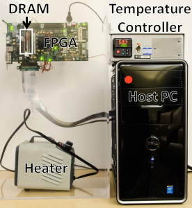
6.2.1 DRAM Test
To achieve the goal of controlling timing parameters, our FPGA test engine supports a list of DRAM commands that get processed directly by the memory controller on the FPGA. Then, on the host PC, we can write a test that specifies a sequence of DRAM commands along with the delay between the commands (i.e., timing parameters). The test sends the commands and delays from the host PC to the FPGA test engine.
Test 2 shows the pseudocode of a test that reads a cache line from a particular bank, row, and column with timing parameters that can be specified by the user. The test first sends an activate to the target row (line 2). After a tRCD delay that we specify (line 3), it sends a read (line 4) to the target cache line. Our test engine enables us to specify the exact delay between two DRAM commands, thus allowing us to tune certain timing parameters. The read delay (tCL) and data transfer latency (tBL) are two DRAM internal timings that cannot be changed using our infrastructure. After our test waits for the data to be fully transferred (line 5), we precharge the bank (line 6) with our specified tRP (line 7). We describe the details of the tests that we created to characterize latency variation of tRCD, tRP, and tRAS in the next few sections.
6.2.2 Characterized DRAM Modules
We characterize latency variation on a total of 30 DDR3 DRAM modules, comprising 240 DRAM chips, from the three major DRAM vendors that hold more than 90% of the market share [30]. Table 6.2.2 lists the relevant information about the tested DRAM modules. All of these modules are dual in-line (i.e., 64-bit data bus) with a single rank of DRAM chips. Therefore, we use the terms DIMM (dual in-line memory module) and module interchangeably. In the rest of the chapter, we refer to a specific DIMM using the label , where and stand for the DIMM number and vendor, respectively. In the table, we group the DIMMs based on their model number, which provides certain information on the process technology and array design used in the chips.
| Vendor | DIMM | Model | Timing (ns) | Assembly |
| Name | (tRCD/tRP/tRAS) | Year | ||
| A Total of 8 DIMMs | M0 | 13.125/13.125/35 | 2013 | |
| M1 | 13.125/13.125/36 | 2012 | ||
| M2 | 13.125/13.125/35 | 2013 | ||
| M3 | 13.125/13.125/35 | 2013 | ||
| B Total of 9 DIMMs | M0 | 13.125/13.125/35 | 2011-12 | |
| M1 | 13.125/13.125/35 | 2012 | ||
| C Total of 13 DIMMs | M0 | 13.125/13.125/34 | 2012 | |
| M1 | 13.125/13.125/36 | 2011 |
6.3 Activation Latency Analysis
In this section, we present our methodology and results on varying the activation latency, which is expressed by the tRCD timing parameter. We first describe the nature of errors caused by tRCD reduction in Section 6.3.1. Then, we describe the FPGA test we conducted on the DRAM modules to characterize tRCD variation in Section 6.3.2. The remaining sections describe different major observations we make based on our results.
6.3.1 Behavior of Activation Errors
As we discuss in Section 2.3, tRCD is defined as the minimum amount of time between the activate and the first column command (read/write). Essentially, tRCD represents the time it takes for a row of sense amplifiers (i.e., the row buffer) to sense and latch a row of data. By employing a lower tRCD value, a column read command may potentially read data from sense amplifiers that are still in the sensing and amplification phase, during which the data has not been fully latched into the sense amplifiers. As a result, reading data with a lowered tRCD can induce timing errors (i.e., flipped bits) in the data.
To further understand the nature of activation errors, we perform experiments to answer two fundamental questions: (i) Does lowering tRCD incur errors on all cache lines read from a sequence of read commands on an opened row? (ii) Do the errors propagate back to the DRAM cells, causing permanent errors for all future accesses?
Errors Localized to First Column Command
To answer the first question, we conduct Test 3 that first activates a row with a specific tRCD value, and then reads every cache line in the entire row. By conducting the test on every row in a number of DIMMs from all three vendors, we make the following observation.
Observation 1: Activation errors are isolated to the cache line from the first read command, and do not appear in subsequently-read cache lines from the same row.
There are two reasons why errors do not occur in the subsequent cache line reads. First, a read accesses only its corresponding sense amplifiers, without accessing the other columns. Hence, a read’s effect is isolated to its target cache line. Second, by the time the second read is issued, a sufficient amount of time has passed for the sense amplifiers to properly latch the data. Note that this observation is independent of DIMMs and vendors as the fundamental DRAM structure is similar across different DIMMs. We discuss the number of activation errors due to different tRCD values for each DIMM in Section 6.3.3.
Activation Errors Propagate into DRAM Cells
To answer our second question, we run two iterations of Test 3 (i.e., reading a row that is activated with a specified tRCD value) on the same row. The first iteration reads a row that is activated with a lower tRCD value, then closes the row. The second iteration re-opens the row using the standard tRCD value, and reads the data to confirm if the errors remain in the cells. Our experiments show that if the first iteration observes activation errors within a cache line, the second iteration observes the same errors. This demonstrates that activation errors not only happen at the sense amplifiers but also propagate back into the cells.
We hypothesize this is because reading a cache line early causes the sense amplifiers to latch the data based on the current bitline voltage. If the bitline voltage has not yet fully developed into or V, the sense amplifier latches in unknown data and amplifies this data to the bitline, which is then restored back into the cell during the restoration phase.
Observation 2: Activation errors occur at the sense amplifiers and propagate back into the cells. The errors persist until the data is overwritten.
After observing that reducing activation latency results in timing errors, we now consider two new questions. First, after how much activation latency reduction do DIMMs start observing timing errors? Second, how many cells experience activation errors at each latency reduction step?
6.3.2 FPGA Test for Activation Latency
To characterize activation errors across every cell in DIMMs, we need to perform an activate and a read on one cache line at a time since activation errors only occur in one cache line per activation. To achieve this, we use Test 4, whose pseudocode is below, for every cache line within a row.
The test iterates through each cache line (lines 2-4) and performs the following steps to test the cache line’s reliability under a reduced tRCD value. First, it opens the row that contains the target cache line, writes a specified data pattern into the cache line, and then precharges the bank (line 5). Second, the test re-opens the row to read the cache line with the standard tRCD (line 6), and verifies if the value was written properly (line 7). Then it precharges the bank again to prepare for the next activate. Third, it re-activates the row using the reduced tRCD value ( in Test 4) to read the target cache line (line 8). It records the number of timing errors (i.e., bit flips) out of the 64-byte (512-bit) cache line (line 9).
In total, we have conducted more than 7500 rounds of tests on the DIMMs shown in Table 6.2.2, accounting for at least 2500 testing hours. For each round of tests, we conducted Test 4 with a different tRCD value and data pattern. We tested five different tRCD values: 12.5ns, 10ns, 7.5ns, 5ns, and 2.5ns. Due to the slow clock frequency of the FPGA, we can adjust timings only at a 2.5ns granularity. We used a set of four different data patterns: 0x00, 0xaa, 0xcc, and 0xff. Each data pattern represents the value that was written into each byte of the entire cache line.
In this dissertation, we do not examine the latency behavior of each cell over a controlled period of time, except for the fact that we perform the tests for multiple rounds per DIMM. The latency of a cell could potentially change over time, within a short period of time (e.g., similar effect as Variable Retention Time) or long period of time (e.g., aging and wearout). However, we leave comprehensive characterization of latency behavior due to time variation as part of future work.
6.3.3 Activation Error Distribution
In this section, we first present the distribution of activation errors collected from all of the tests conducted on every DIMM. Then, we categorize the results by DIMM model to investigate variation across models from different vendors.
Total Bit Error Rates
Figure 6.3 shows the box plots of the bit error rate (BER) observed on every DIMM as tRCD varies. The BER is defined as the fraction of activation error bits in the total population of tested bits. For each box, the bottom, middle, and top lines indicate the 25th, 50th, and 75th percentile of the population. The ends of the whiskers indicate the minimum and maximum BER of all DIMMs for a given tRCD value. Note that the y-axis is in log scale to show low BER values. As a result, the bottom whisker at tRCD=7.5ns cannot be seen due to a minimum value of 0. In addition, we show all observation points for each specific tRCD value by overlaying them on top of their corresponding box. Each point shows a BER collected from one round of Test 4 on one DIMM with a specific data pattern and a tRCD value. Based on these results, we make several observations.
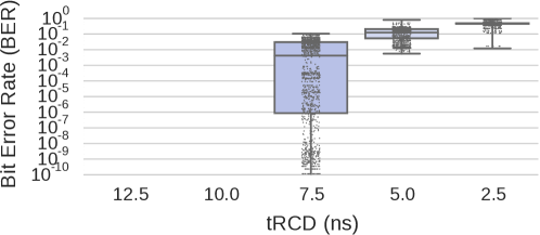
First, we observe that BER exponentially increases as tRCD decreases. With a lower tRCD, fewer sense amplifiers are expected to have enough strength to properly sense the bitline’s voltage value and latch the correct data. Second, at tRCD values of 12.5ns and 10ns, we observe no activation errors on any DIMM. This shows that the tRCD latency of the slowest cells in our tested DIMMs likely falls between 7.5 and 10ns, which are lower than the standard value (13.125ns). The manufacturers use the extra latency as a guardband to provide additional protection against process variation.
Third, the BER variation among DIMMs becomes smaller as tRCD value decreases. The reliability of DIMMs operating at tRCD=7.5ns varies significantly depending on the DRAM models and vendors, as we demonstrate in Section 6.3.3. In fact, some DIMMs have no errors at tRCD=7.5ns, which cannot be seen in the plot due to the log scale. When tRCD reaches 2.5ns, most DIMMs become rife with errors, with a median BER of 0.48, similar to the probability of a coin toss.
Bit Error Rates by DIMM Model
Since the performance of a DIMM can vary across different models, vendors, and fabrication processes, we provide a detailed analysis by breaking down the BER results by DIMM model (listed in Table 6.2.2). Figure 6.4 presents the distribution of every DIMM’s BER grouped by each vendor and model combination. Each box shows the quartiles and median, along with the whiskers indicating the minimum and maximum BERs. Since all of the DIMMs work reliably at 10ns and above, we show the BERs for tRCD=7.5ns and tRCD=5ns.
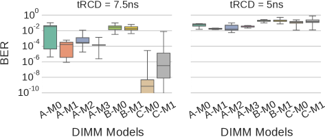
By comparing the BERs across models and vendors, we observe that BER variation exists not only across DIMMs from different vendors, but also on DIMMs manufactured from the same vendor. For example, for DIMMs manufactured by vendor C, Model 0 DIMMs have fewer errors than Model 1 DIMMs. This result suggests that different DRAM models have different circuit architectures or process technologies, causing latency variation between them.
Similar to the observation we made across different DIMM models, we observe variation across DIMMs that have the same model. The variation across DIMMs with the same model can be attributed to process variation due to the imperfect manufacturing process [260, 200, 53, 267]. Our tested results for every DIMM are available online [65].
6.3.4 Impact of Data Pattern
In this section, we investigate the impact of reading different data patterns under different tRCD values. Figure 6.5 shows the average BER of test rounds for three representative DIMMs, one from each vendor, with four data patterns. We do not show the BERs at tRCD=2.5ns, as rows cannot be reliably activated at that latency. We observe that pattern 0x00 is susceptible to more errors than pattern 0xff, while the BERs for patterns 0xaa and 0xcc lie in between.111In a cache line, we write the 8-bit pattern to every byte. This can be clearly seen on , where we observe that 0xff incurs 4 orders of magnitude fewer errors than 0x00 on average at tRCD=7.5ns. We make a similar observation for the rest of the 12 DIMMs from vendor C.
With patterns 0xaa and 0xcc, we observe that bit 0 is more likely to be misread than bit 1. In particular, we examined the flipped bits on three DIMMs that share the same model as , and observed that all of the flipped bits are due to bit 0 flipping to 1. From this observation, we can infer that there is a bias towards bit 1, which can be more reliably read under a shorter activation latency than bit 0.
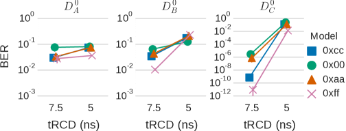
We believe this bias is due to the sense amplifier design. One major DRAM vendor presents a circuit design for a contemporary sense amplifier, and observes that it senses the value on the bitline faster than V [203]. Hence, the sense amplifier is able to sense and latch bit 1 faster than 0. Due to this pattern dependence, we believe that it is promising to investigate asymmetric data encoding or error correction mechanisms that favor 1s over 0s.
Observation 3: Errors caused by reduced activation latency are dependent on the stored data pattern. Reading bit 1 is significantly more reliable than bit 0 at reduced activation latencies.
6.3.5 Effect of Temperature
Temperature is an important external factor that may affect the reliability of DIMMs [301, 85, 210, 160]. In particular, Schroeder et al. [301] and El-Sayed et al. [85] do not observe clear evidence for increasing DRAM error rates with increased temperature in data centers. Other works find that data retention time strongly depends on temperature [160, 210, 287]. However, none of these works have studied the effect of temperature on DIMMs when they are operating with a lower activation latency.
To investigate the impact of temperature on DIMMs operating with an activation latency lower than the standard value, we perform experiments that adjust the ambient temperature using a closed-loop temperature controller (shown in Figure 6.2). Figure 6.6 shows the average BER of three example DIMMs under three temperatures: 20 , 50 , and 70 for tRCD=7.5/5ns. We include error bars, which are computed using 95% confidence intervals.
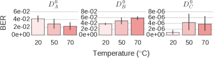
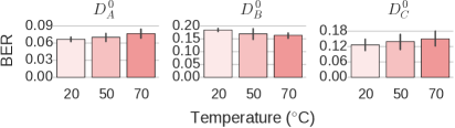
We make two observations. First, at tRCD=7.5ns (Figure 6.6(a)), every DIMM shows a different BER trend as temperature increases. By calculating the p-value between the BERs of different temperatures, we find that the change in BERs is not statistically significant from one temperature to another for two out of the three tested DIMMs, meaning that we cannot conclude that BER increases at higher temperatures. For instance, the p-values between the BERs at 20 and 50 for , , and are 0.084, 0.087, and 0.006, respectively. Two of the three DIMMs have p-values greater than an of 0.05, meaning that the BER change is statistically insignificant. Second, at lower tRCD values (5ns), the difference between the BERs due to temperature becomes even smaller.
Observation 4: Our study does not show enough evidence to conclude that activation errors increase with higher temperatures.
6.3.6 Spatial Locality of Activation Errors
To understand the locations of activation errors within a DIMM, we show the probability of experiencing at least one bit error in each cache line over a large number of experimental runs. We present results of two representative DIMMs from our experiments. Our results on the some other DIMMs are available online [65].
Figures LABEL:fig:rcd_col_err and LABEL:fig:rcd_err_region show the locations of activation errors in all eight banks of two different DIMMs ( and , respectively) using tRCD=7.5ns. The x-axis and y-axis indicate the cache line number and row number (in thousands), respectively. In our tested DIMMs, a row size is 8KB, comprising 128 cache lines (64 bytes). Results are gathered from 40 and 52 iterations of tests for and , respectively. We make two observations.
The first main observation is that errors tend to concentrate at certain regions. Errors in (Figure LABEL:fig:rcd_col_err) cluster at certain columns of cache lines. For the majority of the remaining cache lines in each bank, we observe no errors throughout the experiments. (Figure LABEL:fig:rcd_err_region) shows that the activation errors cluster at certain regions, repeatedly occurring within the first half of the majority of rows. We hypothesize that the cause of such spatial locality of errors is due to the locality of variation in the fabrication process during manufacturing: certain cache line locations can end up with less robust components, such as weaker sense amplifiers, weaker cells, or higher resistance bitlines.
Second, although banks from the same DIMM demonstrate similar patterns of spatial locality of errors, the fraction of errors varies across banks. Some banks observe more errors than other banks. For example, in , Bank 7 experiences more errors than Bank 2. We hypothesize that the variation across banks can be a result of manufacturing process variation, causing certain banks to be more susceptible to reduced activation latency.
Observation 5: Activation errors do not occur uniformly within DRAM. They instead exhibit strong spatial concentration at certain regions.
6.3.7 Density of Activation Errors
In this section, we investigate how errors are distributed within the erroneous cache lines. We present the distribution of error bits at the granularity of data beats, as conventional error-correcting codes (ECC) work at the same granularity. We discuss the effectiveness of employing ECC in Section 6.3.8. Recall from Section 2.3 that a cache line transfer consists of eight 64-bit data beats.
Figure 6.7 shows the distribution of error bits observed in each data beat of all erroneous cache lines when using tRCD=7.5ns. We show experiments from 9 DIMMs, categorized into three DIMM models (one per vendor). We select the model that experiences the lowest average BER from each vendor, and show the frequency of observing 1, 2, 3, and 4 error bits in each data beat. The results are aggregated from all DIMMs of the selected models. We make two observations.
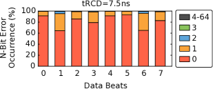
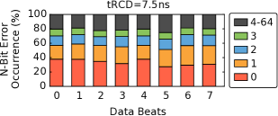
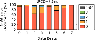
First, most data beats experience fewer than 3 error bits at tRCD=7.5ns. We observe that more than 84%, 53%, and 91% of all the recorded activation errors are just 1-bit errors for DIMMs in A-M1, B-M1, and C-M0, respectively. Across all of the cache lines that contain at least one error bit, 82%, 41%, and 85% of the data beats that make up each cache line have no errors for A-M1, B-M1, and C-M0, respectively. Second, when tRCD is reduced to 5ns, the number of errors increases. The distribution of activation errors in data beats when using tRCD=5ns is available online [65], and it shows that 68% and 49% of data beats in A-M1 and C-M0 still have no more than one error bit.
Observation 6: For cache lines that experience activation errors, the majority of their constituent data beats contain either no errors or just a 1-bit error.
6.3.8 Effect of Error Correction Codes
As shown in the previous section, a majority of data beats in erroneous cache lines contain only a few error bits. In contemporary DRAM, ECC is used to detect and correct errors at the granularity of data beats. Therefore, this creates an opportunity for applying error correction codes (ECC) to correct activation errors. To study of the effect of ECC, we perform an analysis that uses various strengths of ECC to correct activation errors.
Figure 6.8 shows the percentage of cache lines that do not observe any activation errors when using tRCD=7.5ns at various ECC strengths, ranging from single to triple error bit correction. These results are gathered from the same 9 DIMMs used in Section 6.3.7. The first bar of each group is the percentage of cache lines that do not exhibit any activation errors in our experiments. The following data bars show the fraction of error-free cache lines after applying single, double, and triple error correction codes.
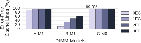
We make two observations. First, without any ECC support, a large fraction of cache lines can be read reliably without any errors in many of the DIMMs we study. Overall, 92% and 99% of cache lines can be read without any activation errors from A-M1 and C-M0 DIMMs, respectively. On the other hand, B-M1 DIMMs are more susceptible to reduced activation latency: only 12% of their cache lines can be read without any activation errors.
Observation 7: A majority of cache lines can be read without any activation errors in most of our tested DIMMs. However, some DIMMs are very susceptible to activation errors, resulting in a small fraction of error-free cache lines.
Second, ECC is effective in correcting the activation errors. For example, with a single error correction code (1EC), which is widely deployed in many server systems, the fraction of reliable cache lines improves from 92% to 99% for A-M1 DIMMs. Even for B-M1 DIMMs, which exhibit activation errors in a large fraction of cache lines, the triple error correcting code is able to improve the percentage of error-free cache lines from 12% to 62%.
Observation 8: ECC is an effective mechanism to correct activation errors, even in modules with a large fraction of erroneous cache lines.
6.4 Precharge Latency Analysis
In this section, we present the methodology and results on varying the precharge latency, represented by the tRP timing parameter. We first describe the nature of timing errors caused by reducing the precharge latency in Section 6.4.1. Then, we describe the FPGA test we conducted to characterize tRP variation in Section 6.4.2. In the remaining sections, we describe four major observations from our result analysis.
6.4.1 Behavior of Precharge Errors
In order to access a new DRAM row, a memory controller issues a precharge command, which performs the following two functions in sequence: (i) it closes the currently-activated row in the array (i.e., it disables the activated row’s wordline); and (ii) it reinitializes the voltage value of every bitline inside the array back to , to prepare for a new activation.
Reducing the precharge latency by a small amount affects only the reinitialization process of the bitlines without interrupting the process of closing the row. The latency of this process is determined by the precharge unit that is placed by each bitline, next to the sense amplifier. By using a tRP value lower than the standard specification, the precharge unit may not have sufficient time to reset the bitline voltage from either (bit 1) or V (bit 0) to , thereby causing the bitline to float at some other intermediate voltage value. As a result, in the subsequent activation, the sense amplifier can incorrectly sense the wrong value from the DRAM cell due to the extra charge left (or lack thereof) on the bitline. We define precharge errors to be timing errors due to reduced precharge latency.
To further understand the nature of precharge errors, we use a test similar to the one for reduced activation latency in Section 6.3.1. The test reduces only the precharge latency, while keeping the activation latency at the standard value, to isolate the effects that occur due to a reduced precharge latency. We answer two fundamental questions: (i) Does lowering the precharge latency incur errors on multiple cache lines in the row activated after the precharge? (ii) Do these errors propagate back to the respective DRAM cells, causing permanent errors for all future accesses to those cells?
Precharge Errors Are Spread Across a Row
Throughout repeated test runs on DIMMs from all three vendors, we observe that reducing the precharge latency induces errors that are spread across multiple cache lines in the row activated after the precharge. This is because reducing the tRP value affects the latency between two row-level DRAM commands, precharge and activate. As a result, having an insufficient amount of precharge time for the array’s bitlines affects the entire row.
Observation 9: Timing errors occur in multiple cache lines in the row activated after a precharge with reduced latency.
Furthermore, these precharge errors are due to the sense amplifiers sensing the wrong voltage on the bitlines, causing them to latch incorrect data. Therefore, as the restoration operation reuses the data latched in the sense amplifiers, the wrong data is written back into the cells, causing the data values in the cells to be corrupted.
6.4.2 FPGA Test for Precharge Latency
In contrast to activation errors, precharge errors are spread across an entire row. As a result, we use a test that varies tRP at the row level. The pseudocode of the test, Test 5, is shown below.
In total, we have conducted more than 4000 rounds of tests on the DIMMs shown in Table 6.2.2, which accounts for at least 1300 testing hours. We use three groups of different data patterns: (0x00, 0xff), (0xaa, 0x33), and (0xcc, 0x55). Each group specifies two different data patterns, which are the inverse of each other, placed in consecutive rows in the same array. This ensures that as we iterate through the rows in order, the partially-precharged state of the bitlines will not favor the data pattern in the adjacent row to be activated.
6.4.3 Precharge Error Distribution
In this section, we first show the distribution of precharge errors collected from all of the tests conducted on every DIMM. Then, we categorize the results by DIMM model to investigate variation across models from different vendors.
Total Bit Error Rates
Figure 6.9 shows the box plots of the BER observed for every DIMM as tRP is varied from 12.5ns down to 2.5ns. Based on these results, we make several observations.
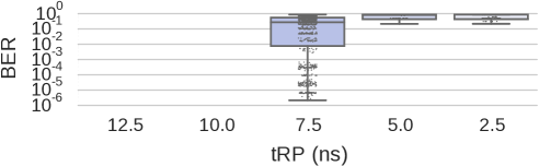
First, similar to the observation made for activation latency, we do not observe errors when the precharge latency is reduced to 12.5 and 10ns, as the reduced latencies are still within the guardband provided. Second, the precharge BER is significantly higher than the activation BER when errors start appearing at 7.5ns – the median of the precharge BER is 587x higher than that of the activation BER (shown in Figure 6.3). This is partially due to the fact that reducing the precharge latency causes the errors to span across multiple cache lines in an entire row, whereas reducing the activation latency affects only the first cache line read from the row. Third, once tRP is set to 5ns, the BER exceeds the tolerable range, resulting in a median BER of 0.43. In contrast, the activation BER does not reach this high an error rate until the activation latency is lowered down to 2.5ns.
Observation 10: With the same amount of latency reduction, the number of precharge errors is significantly higher than the number of activation errors.
Bit Error Rates by DIMM Model
To examine the precharge error trend for individual DIMM models, we show the BER distribution of every DIMM categorized by its model in Figure 6.10. Similar to the observation we made for activation errors in Section 6.3.1, variation exists across different DIMM models. These results provide further support for the existence and prevalence of latency variation in modern DRAM chips.
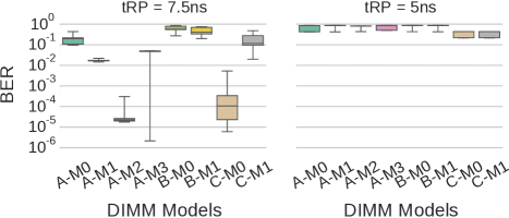
6.4.4 Spatial Locality of Precharge Errors
In this section, we investigate the location and distribution of precharge errors. Due to the large amount of available data, we show representative results from two DIMMs, and from model C-M0. Our results for some DIMMs are available publicly [65]. Figure LABEL:fig:trp_err_loc and Figure LABEL:fig:trp_err_loc_2 show the probability of each cache line seeing at least a one-bit precharge error in all banks of and , respectively, when we set tRP to 7.5ns. The x-axis indicates the cache line number, and the y-axis indicates the row number (in thousands). The results are gathered from 12 iterations of tests. We make several observations based on our results.
First, some banks do not have any precharge errors throughout the experiments, such as Bank 0 (hence the plot is all white). Similar to the activation errors, precharge errors are not distributed uniformly across locations within DIMMs. Second, some banks (e.g., bank 1 in and bank 4 in ) show that the errors concentrate on a certain region of rows, while the other regions experience much fewer or no errors. This demonstrates that certain sense amplifiers, or cells at certain locations are more robust than others, allowing them to work reliably under a reduced precharge latency. Third, similar as our results on activation errors (Section 6.3.7), the fraction of errors varies across banks. We hypothesize the cause of such variation is the manufacturing process variation, leading to different error behavior across banks within the same chip.
Observation 11: Precharge errors do not occur uniformly within DIMMs, but exhibit strong spatial concentration at certain regions.
Overall, we observe that 71.1%, 13.6%, and 84.7% of cache lines contain no precharge errors when they are read from A-M1, B-M1, and C-M0 model DIMMs, respectively, with tRP=7.5ns. Similar to the trend discussed in Section 6.3.8, C-M0 DIMMs have the highest fraction of reliable cache lines among the DIMMs tested, while B-M1 DIMMs experience the largest amount of errors. Even though the number of error-free cache lines at tRP=7.5ns is lower than that at tRCD=7.5ns, the portion is still significant enough to show the prevalence of precharge latency variation in modern DIMMs.
Observation 12: When precharge latency is reduced, a majority of cache lines can be read without any timing errors in some of our tested DIMMs. However, other DIMMs are largely susceptible to precharge errors, resulting in a small fraction of error-free cache lines.
6.5 Restoration Latency Analysis
In this section, we present a methodology and findings on varying the restoration latency, defined by the tRAS timing parameter. First, we elaborate on the impact of reducing tRAS on performance and reliability in Section 6.5.1. Then, we explain our FPGA test conducted to characterize tRAS variation, and present our observations.
6.5.1 Impact of Reduced tRAS
As mentioned in Section 2.3, tRAS specifies the minimum amount of time between issuing an activate and a precharge command to a bank. By reducing tRAS, we can complete an access to one row faster, and quickly switch to access the next row. From the perspective of reliability, reducing the restoration latency may potentially induce errors in the cells due to having insufficient time to restore the lost charge back to the cells. When a row of cells is activated, the cells temporarily lose their charge to the bitlines, so that the sense amplifiers can sense the charge. During the restoration phase, the sense amplifiers restore charge back into the cells, bringing them back to the fully-charged state. By reducing the restoration latency, the amount of restored charge reduces, and the cells may not reach the fully-charged state. As a result, a subsequent access to the same row may not able to sense the correct value, thereby leading to errors.
6.5.2 Test Methodology and Results
To characterize the variation in restoration latency (tRAS), we consider another important factor that affects the amount of charge stored in DRAM cells, which is leakage. DRAM cells lose charge over time, thus requiring a periodic refresh operation to restore the charge. Reducing the restored charge in the cells can cause them to lose too much charge before the next refresh, generating an error.
To perform a conservative characterization, we integrate this leakage factor into our test methodology. We access each row by issuing a pair of commands, activate and precharge, with a specific tRAS value between these two commands. Then, we wait for a full refresh period (defined as 64ms in the DRAM standard [135, 137]) before we access the row again to verify the correctness of its data. We test this sequence on a representative set of DIMMs from all three DRAM vendors and we use four data patterns: 0x00, 0xff, 0xaa, and 0xcc.
In our previously described tests on activation and precharge variation, we test every time step from the default timing value to a minimum value of 2.5ns, with a reduction of 2.5ns per step. Instead of reducing tRAS all the way down to 2.5ns from its standard value of 35ns, we lower it until , which is the latency of activating a row and reading a cache line from it. In a typical situation where the memory controller reads or writes a piece of data after opening a row, lowering tRAS below means that the memory controller can issue a precharge while the data is still being read or written. Doing so risks terminating read or write operations prematurely, causing unknown behavior.
In order to test tRAS with a reasonable range of values, we iterate tRAS from 35ns to . Our is calculated by using the standard tCL=13.125ns and tBL=5ns along with a fast tRCD=5ns. is rounded up to the nearest multiple of 2.5ns, which is 22.5ns.
We do not observe errors across the range of tRAS values we tested in any of our experiments. This implies that charge restoration in modern DRAMs completes within the duration of an activation and a read. Therefore, tRAS can be reduced aggressively without affecting data integrity.
Observation 13: Modern DIMMs have sufficient timing margin to complete charge restoration within the period of an activate and a read. Hence, tRAS can be reduced without introducing any errors.
6.6 Exploiting Latency Variation
Based on our extensive experimental characterization, we propose two new mechanisms to reduce DRAM latency for better system performance. Our mechanisms exploit the key observation that different DIMMs have different amounts of tolerance for lower DRAM latency, and there is a strong correlation between the location of the cells and the lowest latency that the cells can tolerate. The first mechanism (Section 6.6.1) is a pure hardware approach to reducing DRAM latency. The second mechanism (Section 6.6.4) leverages OS support to maximize the benefits of the first mechanism.
6.6.1 Flexible-Latency DRAM
As we discussed in Sections 6.3.6 and 6.4.4, the timing errors caused by reducing the latency of the activation/precharge operations are concentrated on certain DRAM regions, which implies that the latency heterogeneity among DRAM cells exhibits strong locality. Based on this observation, we propose Flexible-LatencY DRAM (FLY-DRAM), a software-transparent design that exploits this heterogeneity in cells to reduce the overall DRAM latency. The key idea of FLY-DRAM is to determine the shortest reliable access latency of each DRAM region, and to use the memory controller to apply that latency to the corresponding DRAM region at runtime. There are two key design challenges of FLY-DRAM, as we discuss below.
The first challenge is determining the shortest access latency. This can be done using a latency profiling procedure, which (i) runs Test 4 (Section 6.3.2) with different timing values and data patterns, and (ii) records the smallest latency that enables reliable access to each region. This procedure can be performed at one of two times. First, the system can run the procedure the very first time the DRAM is initialized, and store the profiling results to non-volatile memory (e.g., disk or flash memory) for future reference. Second, DRAM vendors can run the procedure at manufacturing time, and embed the results in the Serial Presence Detect (SPD) circuitry (a ROM present in each DIMM) [136]. The memory controller can read the profiling results from the SPD circuitry during DRAM initialization, and apply the correct latency for each DRAM region. While the second approach involves a slight modification to the DIMM, it can provide better latency information, as DRAM vendors have detailed knowledge on DRAM cell variation, and can use this information to run more thorough tests to determine a lower bound on the latency of each DRAM region.
The second design challenge is limiting the storage overhead of the latency profiling results. Recording the shortest latency for each cache line can incur a large storage overhead. For example, supporting four different tRCD and tRP timings requires 4 bits per 512-bit cache line, which is almost 0.8% of the entire DRAM storage. Fortunately, the storage overhead can be reduced based on a new observation of ours. As shown in Figures LABEL:fig:rcd_col_err and LABEL:fig:rcd_err_region, timing errors typically concentrate on certain DRAM columns. Therefore, FLY-DRAM records the shortest latency at the granularity of DRAM columns. Assuming we still need 4 bits per DRAM cache line, we need only 512 bits per DRAM bank, or an insignificant 0.00019% storage overhead for the DIMMs we evaluated. One can imagine using more sophisticated structures, such as Bloom Filters [36], to provide finer-grained latency information within a reasonable storage overhead, as shown in prior work on variable DRAM refresh time [211, 287]. We leave this for future work.
The FLY-DRAM memory controller (i) loads the latency profiling results into on-chip SRAMs at system boot time, (ii) looks up the profiled latency for each memory request based on its memory address, and (iii) applies the corresponding latency to the request. By reducing the latency values of tRCD, tRAS, and tRP for some memory requests, FLY-DRAM improves overall system performance, which we quantitatively demonstrate in the next two sections.
6.6.2 Evaluation Methodology
We evaluate the performance of FLY-DRAM on an eight-core system using Ramulator [173, 169], an open-source cycle-level DRAM simulator, driven by CPU traces generated from the Pin dynamic binary instrumentation tool [215]. Our source code is publicly available [65, 169]. Table 7.2 summarizes the configuration of our evaluated system. We use the standard DDR3-1333H timing parameters [135] as our baseline.
| Processor | 8 cores, 3.3 GHz, OoO 128-entry window |
|---|---|
| LLC | 8 MB shared, 8-way set associative |
| DRAM | DDR3-1333H [135], open-row policy [293], |
| 2 channels, 1 rank per channel, 8 banks per rank, | |
| Baseline: tRCD/tCL/tRP = 13.125ns, tRAS = 36ns |
FLY-DRAM Configuration. To conservatively evaluate FLY-DRAM, we use a randomizing page allocator that maps each virtual page to a randomly-located physical page in memory. This allocator essentially distributes memory accesses from an application to different latency regions at random, and is thus unaware of FLY-DRAM regions.
Because each DIMM has a different fraction of fast cache lines, we evaluate FLY-DRAM on three different yet representative real DIMMs that we characterized. We select one DIMM from each vendor. Table 6.3 lists the distribution of cache lines that can be read reliably under different tRCD and tRP values, based on our characterization. For each DIMM, we use its distribution as listed in the table to model the percentage of cache lines with different tRCD and tRP values. For example, for , we set 93% of its cache lines to use a tRCD of 7.5ns, and the remaining 7% of cache lines to use a tRCD of 10ns. Although these DIMMs have a small fraction of cache lines (10%) that can be read using tRCD=5ns, we conservatively set tRCD=7.5ns for them to ensure high reliability. FLY-DRAM dynamically sets tRCD and tRP to either 7.5ns or 10ns for each memory request, based on which cache line the request is to. For the tRAS timing parameter, FLY-DRAM uses 27ns (trcd+tcl) for all cache lines in these three tested DIMMs, as we observe no errors in any of the tested DIMMs due to lowering tRAS (see Section 6.5.2).
| DIMM | Vendor | Model | tRCD Dist. (%) | tRP Dist. (%) | ||
| Name | 7.5ns | 10ns | 7.5ns | 10ns | ||
| A | M1 | 93 | 7 | 74 | 26 | |
| B | M1 | 12 | 88 | 13 | 87 | |
| C | M0 | 99 | 1 | 99 | 1 | |
FLY-DRAM Upper-Bound Evaluation. We also evaluate the upper-bound performance of FLY-DRAM by assuming that every DRAM cell is fast (i.e., 100% of cache lines can be accessed using tRCD/tRP=7.5ns).
Applications and Workloads. To demonstrate the benefits of FLY-DRAM in an 8-core system, we generate 40 8-core multi-programmed workloads by assigning one application to each core. For each 8-core workload, we randomly select 8 applications from the following benchmark suites: SPEC CPU2006 [324], TPC-C/H [348], and STREAM [225]. We use PinPoints [273] to obtain the representative phases of each application. Our simulation executes at least 200 million instructions on each core, as done in prior works on multi-core performance evaluation [332, 242, 172, 193, 108, 60].
Performance Metric. We measure system performance with the weighted speedup (WS) metric [319], which is a measure of job throughput on a multi-core system [86]. Specifically, . is the number of cores in the system. is the IPC of an application that runs on while other applications are running on the other cores. is the IPC of an application when it runs alone in the system without any other applications. Essentially, WS is the sum of every application’s slowdown compared to when it runs alone on the same system.
6.6.3 Multi-Core System Results
Figure 6.11 illustrates the system performance improvement of FLY-DRAM over the baseline for 40 workloads. The x-axis indicates the evaluated DRAM configurations, as shown in Table 6.3. The percentage value on top of each box is the average performance improvement over the baseline. We use box plots to show the performance distribution among all workloads. For each box, the bottom, middle, and top lines indicate the 25th, 50th, and 75th percentile of the population. The ends of the whiskers indicate the minimum and maximum performance improvements. The black dot indicates the means.
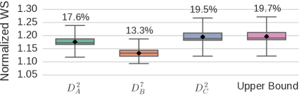
We make the following observations. First, FLY-DRAM improves system performance significantly, by 17.6%, 13.3%, and 19.5% on average across all 40 workloads for the three real DIMMs that we characterize. This is because FLY-DRAM reduces the latency of tRCD, tRP, and tRAS by 42.8%, 42.8%, and 25%, respectively, for many cache lines. In particular, DIMM , whose great majority of cells are reliable at low tRCD and tRP, performs within 1% of the upper-bound performance (19.7% on average). Second, although DIMM has only a small fraction of cells that can operate at 7.5ns, FLY-DRAM still attains significant system performance benefits by using low tRCD and tRP latencies (10ns), which are 23.8% lower than the baseline, for the majority of cache lines. We conclude that FLY-DRAM is an effective mechanism to improve system performance by exploiting the widespread latency variation present across DRAM cells.
6.6.4 Discussion: DRAM-Aware Page Allocator
While FLY-DRAM significantly improves system performance in a software-transparent manner, we can take better advantage of it if we expose the different latency regions of FLY-DRAM to the software stack. We propose the idea of a DRAM-aware page allocator in the OS, whose goal is to better take advantage of FLY-DRAM by intelligently mapping application pages to different-latency DRAM regions in order to improve performance.
Within an application, there is heterogeneity in the access frequency of different pages, where some pages are accessed much more frequently than other pages, as shown in prior works [370, 354, 34, 292, 320, 333, 368]. Our DRAM-aware page allocator places more frequently-accessed pages into lower-latency regions in DRAM. This access frequency aware page placement allows a greater number of DRAM accesses to experience a reduced latency than a page allocator that is oblivious to DRAM latency variation, thereby likely increasing system performance.
For our page allocator to work effectively, it must know which pages are expected to be accessed frequently. In order to convey this information to the page allocator, we extend the OS system calls for memory allocation to take in a Boolean value, which states whether the memory being allocated is expected to be accessed frequently. This information either can be annotated by the programmer, or can be estimated by various dynamic profiling techniques [142, 333, 354, 222, 292, 3, 370, 54, 368]. The page allocator uses this information to find a free physical page in DRAM that suits the expected access frequency of the application page that is being allocated.
We expect that by using our proposed page allocator, FLY-DRAM can perform close to the upper-bound performance reported in Section 6.6.3, even for DIMMs that have a smaller fraction of fast regions. We leave a thorough study of such a page allocator to future work.
6.7 Impact of Technology Scaling
In the previous sections, we demonstrate the existence and various behavior of latency variation in many DIMMs manufactured from year 2011 to 2013. To lower the cost-per-bit and power of DRAM chips, DRAM manufacturers scale down the size of DRAM cells every two years to increase the chip density [340]. Because the performance of DRAM changes with scaling, we set to perform a first-order study on understanding how technology scaling affects the characteristics of latency variation and reliability in DRAM chips.
6.7.1 Methodology
DRAM DIMMs. To study the trend for the three major vendors, we purchase 30 new DDR3L (low-voltage) modules that were manufactured 1) in recent years, between 2014 and 2016, and 2) with double amount of chip density, i.e., 4Gb per chip over the 2Gb chips used in the previous sections. Table 6.4 lists the other related parameters of these DIMMs. For DRAMs manufactured by vendor B, we are able to obtain their technology node size. However, technology node information is not publicly disclosed from the other two vendors.
| Vendor | Tech. | Chip | Assembly | DIMM |
|---|---|---|---|---|
| Node | Density | Year | Counts | |
| A | - | 4Gb | 2016 | 8 |
| B | 29nm | 4Gb | 2015 | 5 |
| B | 28nm | 4Gb | 2015 | 4 |
| C | - | 4Gb | 2014-15 | 13 |
DRAM Tests. We test the DIMMs with Test 4 for tRCD and Test 5 for tRP on our FPGA platform to study latency variation in these DRAM chips. For each DIMM, we performed at least 36 rounds of Test 4 and Test 5. The data patterns used in Tests 4 and 5 are described in Sections 6.3.2 and 6.4.2, respectively. Unless otherwise specified, the testing environment is under an ambient temperature of 201 .
6.7.2 Impact on Activation
Figure 6.12 shows the average BER of DIMMs at each corresponding manufacture year due to various data patterns under a specific tRCD from three major vendor. The error bars denote the 95% confidence intervals. Note that we do not show the results under tRCD =12.5ns because there are no observed errors. We make several major observations.
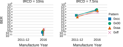
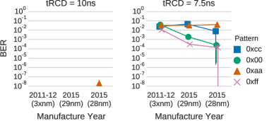
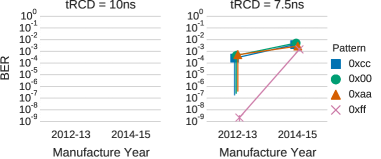
First, Figures 6.12(a)/6.12(b) show that recently manufactured DIMMs of vendors A and B observe a small amount of errors when activation latency is set to 10ns. In contrast, older generation DIMMs do not observe any errors at such activation latency. We believe that this is because DRAM cells fabricated with the latest generations of process technology are becoming more susceptible to process variation and electrical noise as their dimensions are smaller [167]. This means that post-2015 DIMMs consist of more slow cells than DIMMs manufactured in years 2011 and 2012. In contrast to capacity and bandwidth, which improve in newer generation of DIMMs, DRAM access latency needs to increase to ensure data correctness. Our observation shows that DRAM latency is not improving with DRAM scaling, thus becoming a more critical performance bottleneck.
Observation 14: DIMMs manufactured with the latest generation of technology node consist of slower cells that require longer activation latency than the pre-2013 DIMMs.
Second, when activation latency is reduced to 7.5ns, new DIMMs by vendor A and C observe higher BER across all patterns than the old DIMMs, respectively. This implies that newer generation of DIMMs are likely facing worsened activation reliability, thus increasing the number of slow cells.
Third, the BER gaps between the four data patterns become wider as technology scales for vendor B, as shown under tRCD =7.5ns in Figure 6.12(b). The average BER due to 0xaa is at least an order of magnitude higher than that of 0xff for 29nm DIMMs operating at 7.5ns. This pattern dependence is similarly observed for another model of 2015 DIMMs that are manufactured with 28nm – 0xaa induces an order of magnitude higher BER than 0xff. Furthermore, 0xaa is the only pattern that induces errors when rows are activated with tRCD=10ns.
We believe the strong pattern dependence on 0xaa is because storing alternating values (i.e., 0xaa) in consecutive bitlines generates higher bitline-to-bitline coupling noise than the other patterns, as suggested and studied by many prior works [177, 14, 13, 129, 128, 210, 168]. Scaling exacerbates bitline coupling noise during row activation because scaling physically shortens the distance between bitlines, thus amplifying the magnitude of coupling noise.
Observation 15: Data pattern dependence on row activation becomes stronger as technology scales.
6.7.3 Effect of High Temperature
To study the effect of high temperature on new generation DIMMs operating with reduced activation latency, we repeat the same set of DRAM tests on DIMMs placed in high ambient temperature of 70 . Figure 6.13 shows the average BER across all DIMMs, categorized by vendors. The error bars indicate the 95% confidence interval. Since vendor B has two models of DIMMs manufactured with different process technology (i.e., 29 and 28nm), we split vendor B’s DIMMs based on the corresponding technology node information. Figure 6.13(a) and Figure 6.13(b) show the BER results when DIMMs are tested with activation latency (tRCD) of 10ns and 7.5ns, respectively. Several observations can be made from these results.
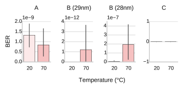
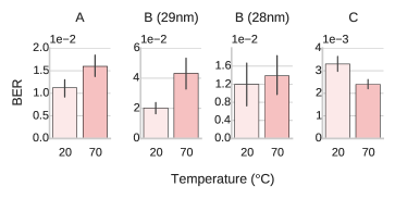
First, when tRCD=10ns (Figure 6.13(a)), DIMMs from both vendor B’s models observe an increase of errors when temperature raises from 20 to 70 . The fraction of slow cells that cannot be activated with 10ns of latency increases due to higher temperature. In particular, raising the temperature to 70 starts inducing a very small fraction of errors in vendor B’s DIMMs that are made with the 29nm node – only () of cells experience bit flips when activated with 10ns on average across all the experiments. For DIMMs made with 28nm, the BER increases by 17x on average under 70 . In contrast, vendor A observes no statistical significant difference in errors induced by low and high temperature – p-value. We do not identify a single bit of error in vendor C’s DIMMs.
Second, under tRCD=7.5ns (Figure 6.13(b)), DIMMs from vendor A, B (29nm) and C observe statistical significant difference in BER when temperature is raised to 70 . The results indicate that the BER increases for vendor A and B. However, vendor C actually sees a small decrease in BER. This anomaly requires further understanding of the DRAM design, which is undisclosed, by vendor C in order to identify the root cause. On the other hand, Vendor B’s 28nm DIMMs observe no statistical difference in BER.
Observation 16: Certain commodity DIMMs require longer activation latency in order for a small fraction of cells to operate reliably under high temperature.
6.7.4 Impact on Precharge
Figure 6.14 shows the average BER of DIMMs at each corresponding manufacture year due to various data patterns under a tRP value of 7.5ns from three major vendor. The error bars denote the 95% confidence intervals. Note that we do not show the results under tRCD =12.5ns because there are no observed errors.
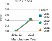
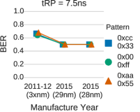
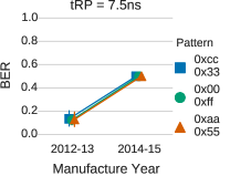
Compared to the older generation, the recently-manufactured DIMMs observe significantly higher average BER at 48%, 50%, and 49% for vendor A, B, and C, respectively. These BER values indicate that the DIMMs become rife with errors, similar to the probability of a coin toss, which exceeds the tolerable range. Furthermore, applying different patterns or high temperature (not shown in the figure) experiences similar BER without significant differences. One reason that reducing tRP has much higher error rate than tRCD is that reducing the tRP value affects the latency between two row-level DRAM commands, precharge and activate. As a result, having an insufficient amount of precharge time for the array’s bitlines affects the entire row, whereas lowering tRCD induces errors only at a cache line level. However, it is unclear why post-2014 generation DIMMs incur much higher error rates than the older generation DIMMs.
Observation 17: The number of precharge errors is significantly higher in the recently manufactured DIMMs than the pre-2014 DIMMs.
6.8 Summary
This chapter provides the first experimental study that comprehensively characterizes and analyzes the latency variation within modern DRAM chips for three fundamental DRAM operations (activation, precharge, and restoration). We find that significant latency variation is present across DRAM cells in all 240 of our tested DRAM chips, and that a large fraction of cache lines can be read reliably even if the activation/restoration/precharge latencies are reduced significantly. Consequently, exploiting the latency variation in DRAM cells can greatly reduce the DRAM access latency. Based on the findings from our experimental characterization, we propose and evaluate a new mechanism, FLY-DRAM (Flexible-LatencY DRAM), which reduces DRAM latency by exploiting the inherent latency variation in DRAM cells. FLY-DRAM reduces DRAM latency by categorizing the DRAM cells into fast and slow regions, and accessing the fast regions with a reduced latency. We demonstrate that FLY-DRAM can greatly reduce DRAM latency, leading to significant system performance improvements on a variety of workloads.
We conclude that it is promising to understand and exploit the inherent latency variation within modern DRAM chips. We hope that the experimental characterization, analysis, and optimization techniques presented in this chapter will enable the development of other new mechanisms that exploit the latency variation within DRAM to improve system performance and perhaps reliability.
Chapter 7 Voltron: Understanding and Exploiting the Trade-off Between Latency and Voltage in DRAM
In the previous chapter, we present our experimental study on characterizing memory latency variation and its reliability implication in real DRAM chips. One important factor that we have not discussed is supply voltage, which significantly impacts DRAM performance and DRAM energy consumption. Our goal in this chapter is to characterize and understand the relationship between supply voltage and DRAM latency. Furthermore, we study the trade-off with various other characteristics of DRAM, including reliability and data retention.
7.1 Background and Motivation
In this section, we first provide necessary DRAM background and terminology. We then discuss related work on reducing the voltage and/or frequency of DRAM, to motivate the need for our study. Figure 7.1(a) shows a high-level overview of a modern memory system organization. A processor (CPU) is connected to a DRAM module via a memory channel, which is a bus used to transfer data and commands between the processor and DRAM. A DRAM module is also called a dual in-line memory module (DIMM) and it consists of multiple DRAM chips, which are controlled together.111In this chapter, we study DIMMs that contain a single rank (i.e., a group of chips in a single DIMM that operate in lockstep). Within each DRAM chip, illustrated in Figure 7.1(b), we categorize the internal components into two broad categories: (i) the DRAM array, which consists of multiple banks of DRAM cells organized into rows and columns, and (ii) peripheral circuitry, which consists of the circuits that sit outside of the DRAM array.
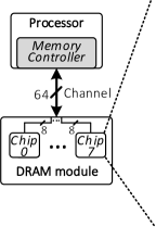
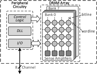
A DRAM array is divided into multiple banks (typically eight in DDR3 DRAM [139, 135]) that can process DRAM commands independently from each other to increase parallelism. A bank contains a 2-dimensional array of DRAM cells. Each cell uses a capacitor to store a single bit of data. Each array of cells is connected to a row of sense amplifiers via vertical wires, called bitlines. This row of sense amplifiers is called the row buffer. The row buffer senses the data stored in one row of DRAM cells and serves as a temporary buffer for the data. A typical row in a DRAM module (i.e., across all of the DRAM chips in the module) is 8KB wide, comprising 128 64-byte cache lines.
The peripheral circuitry has three major components. First, the I/O component is used to receive commands or transfer data between the DRAM chip and the processor via the memory channel. Second, a typical DRAM chip uses a delay-lock loop (DLL) to synchronize its data signal with the external clock to coordinate data transfers on the memory channel. Third, the control logic decodes DRAM commands sent across the memory channel and selects the row and column of cells to read data from or write data into. For a more detailed view of the components in a DRAM chip and how to access data stored in DRAM, we refer the reader to Chapter 2.
7.1.1 Effect of DRAM Voltage and Frequency on Power Consumption
DRAM power is divided into dynamic and static power. Dynamic power is the power consumed by executing the access commands: activate, Phys. Rev. E, and read/write. Each activate and Phys. Rev. Econsumes power in the DRAM array and the peripheral circuitry due to the activity in the DRAM array and control logic. Each read/write consumes power in the DRAM array by accessing data in the row buffer, and in the peripheral circuitry by driving data on the channel. On the other hand, static power is the power that is consumed regardless of the DRAM accesses, and it is mainly due to transistor leakage. DRAM power is governed by both the supply voltage and operating clock frequency: [72]. As shown in this equation, power consumption scales quadratically with supply voltage, and linearly with frequency.
DRAM supply voltage is distributed to both the DRAM array and the peripheral circuitry through respective power pins on the DRAM chip, dedicated separately to the DRAM array and the peripheral circuitry. We call the voltage supplied to the DRAM array, , and the voltage supplied to the peripheral circuitry, . Each DRAM standard requires a specific nominal supply voltage value, which depends on many factors, such as the architectural design and process technology. In this chapter, we focus on the widely used DDR3L DRAM design that requires a nominal supply voltage of 1.35V [139]. To remain operational when the supply voltage is unstable, DRAM can tolerate a small amount of deviation from the nominal supply voltage. In particular, DDR3L DRAM is specified to operate with a supply voltage ranging from 1.283V to 1.45V [236].
The DRAM channel frequency value of a DDR DRAM chip is typically specified using the channel data rate, measured in mega-transfers per second (MT/s). The size of each data transfer is dependent on the width of the data bus, which ranges from 4 to 16 bits for a DDR3L chip [236]. Since a modern DDR channel transfers data on both the positive and the negative clock edges (hence the term double data rate, or DDR), the channel frequency is half of the data rate. For example, a DDR data rate of 1600 MT/s means that the frequency is 800 MHz. To run the channel at a specified data rate, the peripheral circuitry requires a certain minimum voltage () for stable operation. As a result, the supply voltage scales directly (i.e., linearly) with DRAM frequency, and it determines the maximum operating frequency [75, 72].
7.1.2 Memory Voltage and Frequency Scaling
One proposed approach to reducing memory energy consumption is to scale the voltage and/or the frequency of DRAM based on the observed memory channel utilization. We briefly describe two different ways of scaling frequency and/or voltage below.
Frequency Scaling. To enable the power reduction that comes with reduced DRAM frequency, prior works propose to apply dynamic frequency scaling (DFS) by adjusting the DRAM channel frequency based on the memory bandwidth demand from the DRAM channel [75, 74, 73, 277, 31, 336]. A major consequence of lowering the frequency is the likely performance loss that occurs, as it takes a longer time to transfer data across the DRAM channel while operating at a lower frequency. The clocking logic within the peripheral circuitry requires a fixed number of DRAM cycles to transfer the data, since DRAM sends data on each edge of the clock cycle. For a 64-bit memory channel with a 64B cache line size, the transfer typically takes four DRAM cycles [135]. Since lowering the frequency increases the time required for each cycle, the total amount of time spent on data transfer, in nanoseconds, increases accordingly. As a result, not only does memory latency increase, but also memory data throughput decreases, making DFS undesirable to use when the running workload’s memory bandwidth demand or memory latency sensitivity is high. The extra transfer latency from DRAM can also cause longer queuing times for requests waiting at the memory controller [186, 125, 162, 329, 330, 163], further exacerbating the performance loss and potentially delaying latency-critical applications [75, 72].
Voltage and Frequency Scaling. While decreasing the channel frequency reduces the peripheral circuitry power and static power, it does not affect the dynamic power consumed by the operations performed on the DRAM array (i.e., activation, restoration, precharge). This is because DRAM array operations are asynchronous, i.e., independent of the channel frequency [230]. As a result, these operations require a fixed time (in nanoseconds) to complete. For example, the activation latency in a DDR3L DRAM module is 13ns, regardless of the DRAM frequency [236]. If the channel frequency is doubled from 1066 MT/s to 2133 MT/s, the memory controller doubles the number of cycles for the activate timing parameter (i.e., tRCD) (from 7 cycles to 14 cycles), to maintain the 13ns latency.
In order to reduce the dynamic power consumption of the DRAM array as well, prior work proposes dynamic voltage and frequency scaling (DVFS) for DRAM, which reduces the supply voltage along with the channel frequency [72]. This mechanism selects a DRAM frequency based on the current memory bandwidth utilization and finds the minimum operating voltage () for that frequency. is defined to be the lowest voltage that still provides “stable operation” for DRAM (i.e., no errors occur within the data). There are two significant limitations for this proposed DRAM DVFS mechanism. The first limitation is due to a lack of understanding of how voltage scaling affects the DRAM behavior. No prior work provides experimental characterization or analysis of the effect of reducing the DRAM supply voltage on latency, reliability, and data retention in real DRAM chips. As the DRAM behavior under reduced-voltage operation is unknown to satisfactorily maintain the latency and reliability of DRAM, the proposed DVFS mechanism [72] can reduce supply voltage only very conservatively. The second limitation is that this prior work reduces the supply voltage only when it reduces the channel frequency, since a lower channel frequency requires a lower supply voltage for stable operation. As a result, DRAM DVFS results in the same performance issues experienced by the DRAM DFS mechanisms. In Section 7.5.3, we evaluate the main prior work [72] on memory DVFS to quantitatively demonstrate its benefits and limitations.
7.1.3 Our Goal
The goal of this chapter is to (i) experimentally characterize and analyze real modern DRAM chips operating at different supply voltage levels, in order to develop a solid and thorough understanding of how reduced-voltage operation affects latency, reliability, and data retention in DRAM; and (ii) develop a mechanism that can reduce DRAM energy consumption by reducing DRAM voltage, without having to sacrifice memory data throughput, based on the insights obtained from comprehensive experimental characterization. Understanding how DRAM characteristics change at different voltage levels is imperative not only for enabling memory DVFS in real systems, but also for developing other low-power and low-energy DRAM designs that can effectively reduce the DRAM voltage. We experimentally analyze the effect of reducing supply voltage of modern DRAM chips in Section 7.3, and introduce our proposed new mechanism for reducing DRAM energy in Section 7.4.
7.2 Experimental Methodology
To study the behavior of real DRAM chips under reduced voltage, we build an FPGA-based infrastructure based on SoftMC [109], which allows us to have precise control over the DRAM modules. This method was used in many previous works [152, 151, 168, 57, 160, 159, 109, 190, 224, 192, 287, 161, 188, 167, 210] as an effective way to explore different DRAM characteristics (e.g., latency, reliability, and data retention time) that have not been known or exposed to the public by DRAM manufacturers. Our testing platform consists of a Xilinx ML605 FPGA board and a host PC that communicates with the FPGA via a PCIe bus (Figure 7.2). We adjust the supply voltage to the DRAM by using a USB interface adapter [122] that enables us to tune the power rail connected to the DRAM module directly. The power rail is connected to all the power pins of every chip on the module (as shown in Appendix 7.A).
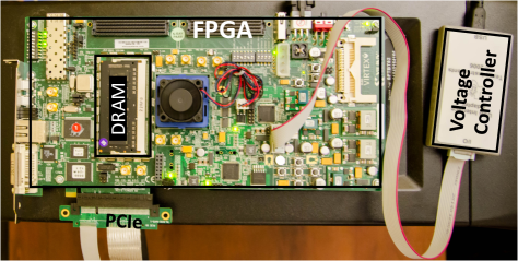
Characterized DRAM Modules. In total, we tested 31 DRAM DIMMs, comprising of 124 DDR3L (low-voltage) chips, from the three major DRAM chip vendors that hold more than 90% of the DRAM market share [30]. Each chip has a 4Gb density. Thus, each of our DIMMs has a 2GB capacity. The DIMMs support up to a 1600 MT/s channel frequency. Due to our FPGA’s maximum operating frequency limitations, all of our tests are conducted at 800 MT/s. Note that the experiments we perform do not require us to adjust the channel frequency. Table 7.1 describes the relevant information about the tested DIMMs. Appendix 7.E provides detailed information on each DIMM. Unless otherwise specified, we test our DIMMs at an ambient temperature of 201 . We examine the effects of high ambient temperature (i.e., 70) in Section 7.3.5.
| Vendor | Total Number | Timing (ns) | Assembly |
|---|---|---|---|
| of Chips | (tRCD/tRP/tRAS) | Year | |
| A (10 DIMMs) | 40 | 13.75/13.75/35 | 2015-16 |
| B (12 DIMMs) | 48 | 13.75/13.75/35 | 2014-15 |
| C (9 DIMMs) | 36 | 13.75/13.75/35 | 2015 |
DRAM Tests. At a high level, we develop a test (Test 6) that writes/reads data to/from every row in the entire DIMM, for a given supply voltage. The test takes in several different input parameters: activation latency (tRCD), precharge latency (tRP), and data pattern. The goal of the test is to examine if any errors occur under the given supply voltage with the different input parameters.
In the test, we iteratively test two consecutive rows at a time. The two rows hold data that are the inverse of each other (i.e., and ). Reducing tRP lowers the amount of time the precharge unit has to reset the bitline voltage from either full voltage (bit value 1) or zero voltage (bit value 0) to half voltage. If tRP were reduced too much, the bitlines would float at some other intermediate voltage value between half voltage and full/zero voltage. As a result, the next activation can potentially start before the bitlines are fully precharged. If we were to use the same data pattern in both rows, the sense amplifier would require less time to sense the value during the next activation, as the bitline is already biased toward those values. By using the inverse of the data pattern in the row that is precharged for the next row that is activated, we ensure that the partially-precharged state of the bitlines does not unfairly favor the access to the next row [57]. In total, we use three different groups of data patterns for our test: (0x00, 0xff), (0xaa, 0x33), and (0xcc, 0x55). Each specifies the and , placed in consecutive rows in the same bank.
7.3 Characterization of DRAM Under Reduced Voltage
In this section, we present our major observations from our detailed experimental characterization of 31 commodity DIMMs (124 chips) from three vendors, when the DIMMs operate under reduced supply voltage (i.e., below the nominal voltage level specified by the DRAM standard). First, we analyze the reliability of DRAM chips as we reduce the supply voltage without changing the DRAM access latency (Section 7.3.1). Our experiments are designed to identify if lowering the supply voltage induces bit errors (i.e., bit flips) in data. Second, we present our findings on the effect of increasing the activation and precharge latencies for DRAM operating under reduced supply voltage (Section 7.3.2). The purpose of this experiment is to understand the trade-off between access latencies (which impact performance) and the supply voltage of DRAM (which impacts energy consumption). We use detailed circuit-level DRAM simulations to validate and explain our observations on the relationship between access latency and supply voltage. Third, we examine the spatial locality of errors induced due to reduced-voltage operation (Section 7.3.3) and the distribution of errors in the data sent across the memory channel (Section 7.3.4). Fourth, we study the effect of temperature on reduced-voltage operation (Section 7.3.5). Fifth, we study the effect of reduced voltage on the data retention times within DRAM (Section 7.3.6). We present a summary of our findings in Section 7.3.7.
7.3.1 DRAM Reliability as Supply Voltage Decreases
We first study the reliability of DRAM chips under low voltage, which was not studied by prior works on DRAM voltage scaling (e.g., [72]). For these experiments, we use the minimum activation and precharge latencies that we experimentally determine to be reliable (i.e., they do not induce any errors) under the nominal voltage of 1.35V at 201 temperature. As shown in prior works [57, 192, 55, 190, 109, 188, 211, 4, 287, 353, 33, 204, 266, 272, 160, 159, 161], DRAM manufacturers adopt a pessimistic standard latency that incorporates a large margin as a safeguard to ensure that each chip deployed in the field operates correctly under a wide range of conditions. Examples of these conditions include process variation, which causes some chips or some cells within a chip to be slower than others, or high operating temperatures, which can affect the time required to perform various operations within DRAM. Since our goal is to understand how the inherent DRAM latencies vary with voltage, we conduct our experiments without such an excessive margin. We identify that the reliable tRCD and tRP latencies are both 10ns (instead of the 13.75ns latency specified by the DRAM standard) at 20 , which agree with the values reported by prior work on DRAM latency characterization [57, 192, 188].
Using the reliable minimum latency values (i.e., 10ns for all of the DIMMs), we run Test 6, which accesses every bit within a DIMM at the granularity of a 64B cache line. In total, there are 32 million cache lines in a 2GB DIMM. We vary the supply voltage from the nominal voltage of 1.35V down to 1.20V, using a step size of 0.05V (50mV). Then, we change to a smaller step size of 0.025V (25mV), until we reach the lowest voltage at which the DIMM can operate reliably (i.e., without any errors) while employing the reliable minimum latency values. (We examine methods to further reduce the supply voltage in Section 7.3.2.) For each voltage step, we run 30 rounds of Test 6 for each DIMM. Figure 7.3 shows the fraction of cache lines that experience at least 1 bit of error (i.e., 1 bit flip) in each DIMM (represented by each curve), categorized based on vendor.
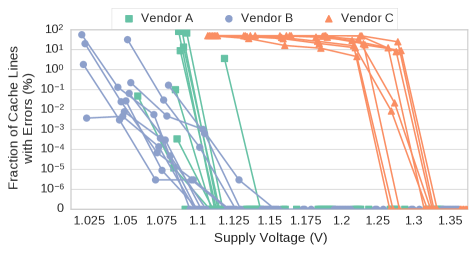
We make three observations. First, when each DIMM runs below a certain voltage level, errors start occurring. We refer to the minimum voltage level of each DIMM that allows error-free operation as . For example, most DIMMs from Vendor C have . Below , we observe errors because the fundamental DRAM array operations (i.e., activation, restoration, precharge) cannot fully complete within the time interval specified by the latency parameters (e.g., tRCD, tRAS) at low voltage. Second, not all cache lines exhibit errors for all supply voltage values below . Instead, the number of erroneous cache lines for each DIMM increases as we reduce the voltage further below . Specifically, Vendor A’s DIMMs experience a near-exponential increase in errors as the supply voltage reduces below . This is mainly due to the manufacturing process and architectural variation, which introduces strength and size variation across the different DRAM cells within a chip [166, 200, 57, 190, 192, 55, 188, 167]. Third, variation in exists not only across DIMMs from different vendors, but also across DIMMs from the same vendor. However, the variation across DIMMs from the same vendor is much smaller compared to cross-vendor variation, since the fabrication process and circuit designs can differ drastically across vendors. These results demonstrate that reducing voltage beyond , without altering the access latency, has a negative impact on DRAM reliability.
We also conduct an analysis of storing different data patterns on the error rate during reduced-voltage operation (see Appendix 7.B). In summary, our results show that the data pattern does not have a consistent effect on the rate of errors induced by reduced-voltage operation. For most supply voltage values, the data pattern does not have a statistically significant effect on the error rate.
Source of Errors. To understand why errors occur in data as the supply voltage reduces below , we perform circuit-level SPICE simulations [253, 223], which reveal more detail on how the cell arrays operate. We develop a SPICE model of the DRAM array that uses a sense amplifier design from prior work [29] with the transistor model from the Predictive Technology Model (PTM) [282, 378]. Appendix 7.C provides a detailed description of our SPICE simulation model, which we have open-sourced [2].
We vary the supply voltage of the DRAM array () in our SPICE simulations from 1.35V to 0.90V. Figure 7.4 shows the bitline voltage during activation and precharge for different values. Times 0ns and 50ns correspond to when the DRAM receives the activate and the Phys. Rev. Ecommands, respectively. An activate causes the bitline voltage to increase from to in order to sense the stored data value of “1”. A Phys. Rev. Eresets the bitline voltage back to in order to enable the issuing of a later activate to another row within the same bank. In the figure, we mark the points where the bitline reaches the ready-to-access voltage, which we assume to be 75% of ; ready-to-precharge voltage, which we assume to be 98% of ; and ready-to-activate voltage, which we assume to be within 2% of . These points represent the minimum tRCD, tRAS, and tRP values, respectively, required for reliable DRAM operation. For readers who wish to understand the bitline voltage behavior in more detail, we refer them to recent works [192, 193, 108, 190, 188] that provide extensive background on how the bitline voltage changes during the three DRAM operations.
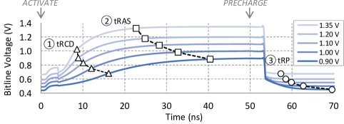
We make two observations from our SPICE simulations. First, we observe that the bitline voltage during activation increases at a different rate depending on the supply voltage of the DRAM array (). Thus, the supply voltage affects the latency of the three DRAM operations (activation, restoration, and precharge). When the nominal voltage level (1.35V) is used for , the time (tRCD) it takes for the sense amplifier to drive the bitline to the ready-to-access voltage level (75% of ) is much shorter than the time to do so at a lower . As decreases, the sense amplifier needs more time to latch in the data, increasing the activation latency. Similarly, the restoration latency (tRAS) and the precharge latency (tRP) increase as decreases.
Second, the latencies of the three fundamental DRAM array operations (i.e., activation, restoration, precharge) do not correlate with the channel (or clock) frequency (not shown in Figure 7.4). This is because these operations are clock-independent asynchronous operations that are a function of the cell capacitance, bitline capacitance, and [158].222In Appendix 7.C, we show a detailed circuit schematic of a DRAM array that operates asynchronously, which forms the basis of our SPICE circuit simulation model [2]. As a result, the channel frequency is independent of the three fundamental DRAM operations.
Therefore, we hypothesize that DRAM errors occur at lower supply voltages because the three DRAM array operations have insufficient latency to fully complete at lower voltage levels. In the next section, we experimentally investigate the effect of increasing latency values as we vary the supply voltage on real DRAM chips.
7.3.2 Longer Access Latency Mitigates Voltage-Induced Errors
To confirm our hypothesis from Section 7.3.1 that a lower supply voltage requires a longer access latency, we test our DIMMs at supply voltages below the nominal voltage (1.35V) while incrementally increasing the activation and precharge latencies to be as high as 20ns (2x higher than the tested latency in Section 7.3.1). At each supply voltage value, we call the minimum required activation and precharge latencies that do not exhibit any errors and , respectively.
Figure 7.5 shows the distribution of (top row) and (bottom row) measured for all DIMMs across three vendors as we vary the supply voltage. Each circle represents a or value. A circle’s size indicates the DIMM population size, with bigger circles representing more DIMMs. The number above each circle indicates the fraction of DIMMs that work reliably at the specified voltage and latency. Also, we shade the range of potential and values. Since our infrastructure can adjust the latencies at a granularity of 2.5ns, a or value of 10ns is only an approximation of the minimum value, as the precise or falls between 7.5ns and 10ns. We make three major observations.
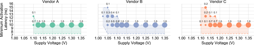
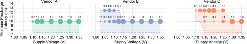
First, when the supply voltage falls below 333In Section 7.3.1, we define as the minimum voltage level of each DIMM that allows error-free operation. Table 7.E in Appendix 7.E shows the value we found for each DIMM., the tested DIMMs show that an increase of at least 2.5ns is needed for and to read data without errors. For example, some DIMMs require at least a 2.5ns increase of or to read data without errors at 1.100V, 1.125V, and 1.25V from Vendors A, B, and C, respectively. Since our testing platform can only identify the minimum latency at a granularity of 2.5ns [109], we use circuit-level simulations to obtain a more precise latency measurement of and (which we describe in the latter part of this section).
Second, DIMMs from different vendors exhibit very different behavior on how much and need to increase for reliable operation as supply voltage falls below . Compared to other vendors, many more of Vendor C’s DIMMs require higher and to operate at a lower . This is particularly the case for the precharge latency, . For instance, 60% of Vendor C’s DIMMs require a of 12.5ns to read data without errors at 1.25V, whereas this increase is not necessary at all for DIMMs from Vendor A, which all operate reliably at 1.15V. This reveals that different vendors may have different circuit architectures or manufacturing process technologies, which lead to variations in the additional latency required to compensate for a reduced in DIMMs.
Third, at very low supply voltages, not all of the DIMMs have valid and values less than or equal to 20ns that enable error-free operation of the DIMM. We see that the circle size gets smaller as the supply voltage reduces, indicating that the number of DIMMs that can operate reliably (even at higher latency) reduces. For example, Vendor A’s DIMMs can no longer operate reliably (i.e., error-free) when the voltage is below 1.1V. We tested a small subset of DIMMs with latencies of more than 50ns and found that these very high latencies still do not prevent errors from occurring. We hypothesize that this is because of signal integrity issues on the channel, causing bits to flip during data transfer at very low supply voltages.
We correlate our characterization results with our SPICE simulation results from Section 7.3.1, demonstrating that there is a direct relationship between supply voltage and access latency. This new observation on the trade-off between supply voltage and access latency is not discussed or demonstrated in prior work on DRAM voltage scaling [72], where the access latency (in nanoseconds) remains fixed when performing memory DVFS. In conclusion, we demonstrate both experimentally and in circuit simulations that increasing the access latency (i.e., tRCD and tRP) allows us to lower the supply voltage while still reliably accessing data without errors.
Deriving More Precise Access Latency Values. One limitation of our experiments is that we cannot precisely measure the exact and values, due to the 2.5ns minimum latency granularity of our experimental framework [109]. Furthermore, supply voltage is a continuous value, and it would take a prohibitively long time to study the supply voltage experimentally at a finer granularity. We address these limitations by enriching our experimental results with circuit-level DRAM SPICE simulations that model a DRAM array (see Appendix 7.C for details of our circuit simulation model).
The SPICE simulation results highly depend on the specified transistor parameters (e.g., transistor width). To fit our SPICE results with our experimental results (for the supply voltage values that we studied experimentally), we manually adjust the transistor parameters until the simulated results fit within our measured range of latencies. Figure 7.6 shows the latencies reported for activation and precharge operations using our final SPICE model, based on the measured experimental data for Vendor B.
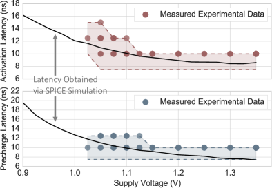
We make two major observations. First, we see that the SPICE simulation results fit within the range of latencies measured during our experimental characterization, confirming that our simulated circuit behaves close to the real DIMMs. As a result, our circuit model allows us to derive a more precise minimum latency for reliable operation than our experimental data.444The circuit model can further serve as a common framework for studying other characteristics of DRAM. Second, DRAM arrays can operate at a wide range of voltage values without experiencing errors. This aligns with our hypothesis that errors at very low supply voltages (e.g., 1V) occur during data transfers across the channel rather than during DRAM array operations. Therefore, our SPICE simulations not only validate our observation that a lower supply voltage requires longer access latency, but also provide us with a more precise reliable minimum operating latency estimate for a given supply voltage.
7.3.3 Spatial Locality of Errors
While reducing the supply voltage induces errors when the DRAM latency is not long enough, we also show that not all DRAM locations experience errors at all supply voltage levels. To understand the locality of the errors induced by a low supply voltage, we show the probability of each DRAM row in a DIMM experiencing at least one bit of error across all experiments. We present results for two representative DIMMs from two different vendors, as the observations from these two DIMMs are similar to those we make for the other tested DIMMs. Our results collected from each of the 31 DIMMs are publicly available [2].
Figure 7.7 shows the probability of each row experiencing at least a one-bit error due to reduced voltage in the two representative DIMMs. For each DIMM, we choose the supply voltage when errors start appearing (i.e., the voltage level one step below ), and we do not increase the DRAM access latency (i.e., 10ns for both tRCD and tRP). The x-axis and y-axis indicate the bank number and row number (in thousands), respectively. Our tested DIMMs are divided into eight banks, and each bank consists of 32K rows of cells.555Additional results showing the error locations at different voltage levels are in Appendix 7.D.
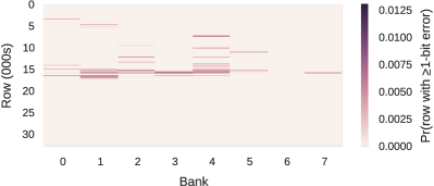
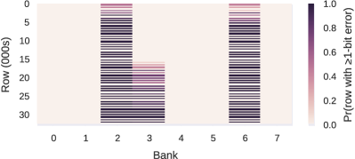
Our main observation is that errors tend to cluster at certain locations. For our representative DIMMs, we see that errors tend to cluster at certain rows across multiple banks for Vendor B. On the contrary, Vendor C’s DIMMs exhibit errors in certain banks but not in other banks. We hypothesize that the error concentration can be a result of (i) manufacturing process variation, resulting in less robust components at certain locations, as observed in Vendor B’s DIMMs; or (ii) architectural design variations in the power delivery network. However, it is hard to verify our hypotheses without knowing the specifics of the DRAM circuit design, which is proprietary information that varies across different DRAM models within and across vendors.
Another implication of the spatial concentration of errors under low voltage is that only those regions with errors require a higher access latency to read or write data correctly, whereas error-free regions can be accessed reliably with the standard latency. In Section 7.5.5, we discuss and evaluate a technique that exploits this spatial locality of errors to improve system performance.
7.3.4 Density of Errors
In this section, we investigate the density (i.e., the number) of error bits that occur within each data beat (i.e., the unit of data transfer, which is 64 bits, through the data bus) read back from DRAM. Conventional error-correcting codes (ECC) used in DRAM detect and correct errors at the granularity of a data beat. For example, SECDED ECC [321, 218] can correct a single-bit error and detect two-bit errors within a data beat. Figure 7.8 shows the distribution of data beats that contain no errors, a single-bit error, two-bit errors, or more than two bits of errors, under different supply voltages for all DIMMs. These distributions are collected from 30 rounds of experiments that were tested on each of the 31 DIMMs per voltage level, using 10ns of activation and precharge latency. A round of experiment refers to a single run of Test 6, as described in Section 7.2, on a specified DIMM.
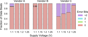
The results show that lowering the supply voltage increases the fraction of beats that contain more than two bits of errors. There are very few beats that contain only one or two error bits. This implies that the most commonly-used ECC scheme, SECDED, is unlikely to alleviate errors induced by a low supply voltage. Another ECC mechanism, Chipkill [321, 218], protects multiple bit failures within a DRAM chip. However, it cannot correct errors in multiple DRAM chips. Instead, we believe that increasing the access latency, as shown in Section 7.3.2, is a more effective way of eliminating errors under low supply voltages.
7.3.5 Effect of Temperature
Temperature is an important external factor that can affect the behavior of DRAM [301, 85, 210, 160, 192, 211, 168, 188]. Prior works have studied the impact of temperature on reliability [301, 85, 168, 167], latency [192, 57, 188], and retention time [160, 210, 211, 287] at the nominal supply voltage. However, no prior work has studied the effect of temperature on the latency at which DRAM operates reliably, as the supply voltage changes.
To reduce the test time, we test 13 representative DIMMs under a high ambient temperature of 70 using a closed-loop temperature controller [109]. Figure 7.9 shows the and values of tested DIMMs, categorized by vendor, at 20 and 70 . The error bars indicate the minimum and maximum latency values across all DIMMs we tested that are from the same vendor. We increase the horizontal spacing between the low and high temperature data points at each voltage level to improve readability.
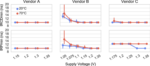
We make two observations. First, temperature impacts vendors differently. On Vendor A’s DIMMs, temperature does not have an observable impact on the reliable operation latencies. Since our platform can test latencies with a step size of only 2.5ns, it is possible that the effect of high temperature on the reliable minimum operating latency for Vendor A’s DIMMs may be within 2.5ns. On the other hand, the temperature effect on latency is measurable on DIMMs from Vendors B and C. DIMMs from Vendor B are not strongly affected by temperature when the supply voltage is above 1.15V. The precharge latency for Vendor C’s DIMMs is affected by high temperature at supply voltages of 1.35V and 1.30V, leading to an increase in the minimum latency from 10ns to 12.5ns. When the voltage is below 1.25V, the impact of high temperature on precharge latency is not observable, as the precharge latency already needs to be raised by 2.5ns, to 12.5ns, at 20 . Second, the precharge latency is more sensitive to temperature than the activation latency. Across all of our tested DIMMs, tRP increases with high temperature under a greater number of supply voltage levels, whereas tRCD is less likely to be perturbed by temperature.
7.3.6 Impact on Refresh Rate
Recall from Chapter 2 that a DRAM cell uses a capacitor to store data. The charge in the capacitor leaks over time. To prevent data loss, DRAM periodically performs an operation called refresh to restore the charge stored in the cells. The frequency of refresh is determined by the amount of time a cell can retain enough charge without losing information, commonly referred to as a cell’s retention time. For DDR3 DIMMs, the worst-case retention time assumed for a DRAM cell is 64ms (or 32ms at temperatures above 85 [210, 211]). Hence, each cell is refreshed every 64ms, which is the DRAM-standard refresh interval.
When we reduce the supply voltage of the DRAM array, we expect the retention time of a cell to decrease, as less charge is stored in each cell. This could potentially require a shorter refresh interval (i.e., more frequent refreshes). To investigate the impact of low supply voltage on retention time, our experiment writes all 1s to every cell, and reads out the data after a given amount of retention time, with refresh disabled. We test a total of seven different retention times (in ms): 64 (the standard time), 128, 256, 512, 1024, 1536, and 2048. We conduct the experiment for ten rounds on every DIMM from all three vendors. Figure 7.10 shows the average number of weak cells (i.e., cells that experience bit flips due to too much leakage at a given retention time) across all tested DIMMs, for each retention time, under both 20 and 70 . We evaluate three voltage levels, 1.35V, 1.2V, and 1.15V, that allow data to be read reliably with a sufficiently long latency. The error bars indicate the 95% confidence interval. We increase the horizontal spacing between the curves at each voltage level to improve readability.
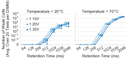
Our results show that every DIMM can retain data for at least 256ms before requiring a refresh operation, which is 4x higher than the standard worst-case specification. These results align with prior works, which also experimentally demonstrate that commodity DRAM cells have much higher retention times than the standard specification of 64ms [166, 210, 160, 192, 109, 188, 272, 287]. Even though higher retention times (i.e., longer times without refresh) reveal more weak cells, the number of weak cells is still very small, e.g., tens of weak cells out of billions of cells, on average across all DIMMs at under 20 . Again, this corresponds closely to observations from prior works showing that there are relatively few weak cells with low retention time in DRAM chips, especially at lower temperatures [166, 210, 160, 192, 109, 287, 188, 272].
We observe that the effect of the supply voltage on retention times is not statistically significant. For example, at a 2048ms retention time, the average number of weak cells in a DRAM module increases by only 9 cells (out of a population of billions of cells) when the supply voltage drops from 1.35V (66 weak cells) to 1.15V (75 weak cells) at . For the same 2048ms retention time at , the average number of weak cells increases by only 131 cells when the supply voltage reduces from 1.35V (2510 weak cells) to 1.15V (2641 weak cells).
When we lower the supply voltage, we do not observe any weak cells until a retention time of 512ms, which is 8x the standard refresh interval of 64ms. Therefore, we conclude that using a reduced supply voltage does not require any changes to the standard refresh interval at 20 and 70 ambient temperature.
7.3.7 Summary
We have presented extensive characterization results and analyses on DRAM chip latency, reliability, and data retention time behavior under various supply voltage levels. We summarize our findings in six key points. First, DRAM reliability worsens (i.e., more errors start appearing) as we reduce the supply voltage below . Second, we discover that voltage-induced errors occur mainly because, at low supply voltages, the DRAM access latency is no longer sufficient to allow the fundamental DRAM operations to complete. Third, via both experiments on real DRAM chips and SPICE simulations, we show that increasing the latency of activation, restoration, and precharge operations in DRAM can mitigate errors under low supply voltage levels until a certain voltage level. Fourth, we show that voltage-induced errors exhibit strong spatial locality in a DRAM chip, clustering at certain locations (i.e., certain banks and rows). Fifth, temperature affects the reliable access latency at low supply voltage levels and the effect is very vendor-dependent. Sixth, we find that reducing the supply voltage does not require increasing the standard DRAM refresh rate for reliable operation below 70 .
7.4 Voltron: Reducing DRAM Energy Without Sacrificing Memory Throughout
Based on the extensive understanding we developed on reduced-voltage operation of real DRAM chips in Section 7.3, we propose a new mechanism called Voltron, which reduces DRAM energy without sacrificing memory throughput. Voltron exploits the fundamental observation that reducing the supply voltage to DRAM requires increasing the latency of the three DRAM operations in order to prevent errors. Using this observation, the key idea of Voltron is to use a performance model to determine by how much to reduce the DRAM supply voltage, without introducing errors and without exceeding a user-specified threshold for performance loss. Voltron consists of two main components: (i) array voltage scaling, a hardware mechanism that leverages our experimental observations to scale only the voltage supplied to the DRAM array; and (ii) performance-aware voltage control, a software mechanism666Note that this mechanism can also be implemented in hardware, or as a cooperative hardware/software mechanism. that automatically chooses the minimum DRAM array voltage that meets a user-specified performance target.
7.4.1 Array Voltage Scaling
As we discussed in Section 7.1.1, the DRAM supply voltage to the peripheral circuitry determines the maximum operating frequency. If we reduce the supply voltage directly, the frequency needs to be lowered as well. As more applications become more sensitive to memory bandwidth, reducing DRAM frequency can result in a substantial performance loss due to lower data throughput. In particular, we find that reducing the DRAM frequency from 1600 MT/s to 1066 MT/s significantly degrades performance of our evaluated memory-intensive applications by 16.1%. Therefore, the design challenge of Voltron is to reduce the DRAM supply voltage without changing the DRAM frequency.
To address this challenge, the key idea of Voltron’s first component, array voltage scaling, is to reduce the voltage supplied to the DRAM array () without changing the voltage supplied to the peripheral circuitry, thereby allowing the DRAM channel to maintain a high frequency while reducing the power consumption of the DRAM array. To prevent errors from occurring during reduced-voltage operation, Voltron increases the latency of the three DRAM operations (activation, restoration, and precharge) in every DRAM bank based on our observations in Section 7.3.
By reducing , we effectively reduce (i) the dynamic DRAM power on activate, precharge, and refresh operations; and (ii) the portion of the static power that comes from the DRAM array. These power components decrease quadratically with the square of the array voltage reduction in a modern DRAM chip [158, 29]. The trade-off is that reducing requires increasing the latency of the three DRAM operations, for reliable operation, thereby leading to some system performance degradation, which we quantify in our evaluation (Section 7.5).
7.4.2 Performance-Aware Voltage Control
Array voltage scaling provides system users with the ability to decrease to reduce DRAM power. Employing a lower provides greater power savings, but at the cost of longer DRAM access latency, which leads to larger performance degradation. This trade-off varies widely across different applications, as each application has a different tolerance to the increased memory latency. This raises the question of how to pick a “suitable” array voltage level for different applications as a system user or designer. For this dissertation, we say that an array voltage level is suitable if it does not degrade system performance by more than a user-specified threshold. Our goal is to provide a simple technique that can automatically select a suitable value for different applications. To this end, we propose performance-aware voltage control, a power-performance management policy that selects a minimum that satisfies a desired performance constraint. The key observation is that an application’s performance loss (due to increased memory latency) scales linearly with the application’s memory demand (e.g., memory intensity). Based on this empirical observation we make, we build a performance loss predictor that leverages a linear model to predict an application’s performance loss based on its characteristics at runtime. Using the performance loss predictor, Voltron finds a that can keep the predicted performance within a user-specified target at runtime.
Key Observation. We find that an application’s performance loss due to higher latency has a strong linear relationship with its memory demand (e.g., memory intensity). Figure 7.11 shows the relationship between the performance loss of each application (due to reduced voltage) and its memory demand under two different reduced-voltage values (see Section 7.5.1 for our methodology). Each data point represents a single application. Figure 7.11(a) shows each application’s performance loss versus its memory intensity, expressed using the commonly-used metric MPKI (last-level cache misses per kilo-instruction). Figure 7.11(b) shows each application’s performance loss versus its memory stall time, the fraction of execution time for which memory requests stall the CPU’s instruction window (i.e., reorder buffer). In Figure 7.11(a), we see that the performance loss is a piecewise linear function based on the MPKI. The observation that an application’s sensitivity to memory latency is correlated with MPKI has also been made and utilized by prior works [170, 171, 249, 380, 248, 242, 69, 70, 352, 376, 71].
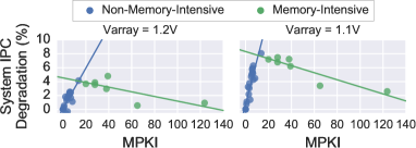
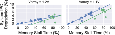
When an application is not memory-intensive (i.e., has an ), its performance loss grows linearly with MPKI, becoming more sensitive to memory latency. Latency-sensitive applications spend most of their time performing computation at the CPU cores and issue memory requests infrequently. As a result, increasing the number of memory requests causes more stall cycles in the CPU.
On the other hand, the performance of memory-intensive applications (i.e., those with ) is less sensitive to memory latency as the MPKI grows. This is because memory-intensive applications experience frequent cache misses and spend a large portion of their time waiting on pending memory requests. As a result, their rate of progress is significantly affected by the memory bandwidth, and therefore they are more sensitive to memory throughput instead of latency. With more outstanding memory requests (i.e., higher MPKI), the memory system is more likely to service them in parallel, leading to more memory-level parallelism [171, 249, 95, 250, 247, 187]. Therefore, improved memory-level parallelism enables applications to tolerate higher latencies more easily.
Figure 7.11(b) shows that an application’s performance loss increases with its instruction window (reorder buffer) stall time fraction due to memory requests for both memory-intensive and non-memory-intensive applications. A stalled instruction window prevents the CPU from fetching or dispatching new instructions [250], thereby degrading the running application’s performance. This observation has also been made and utilized by prior works [94, 247, 245, 250].
Performance Loss Predictor. Based on the observed linear relationships between performance loss vs. MPKI and memory stall time fraction, we use ordinary least squares (OLS) regression to develop a piecewise linear model for each application that can serve as the performance loss predictor for Voltron. Equation 7.1 shows the model, which takes the following inputs: memory latency (), the application’s MPKI, and its memory stall time fraction.
| (7.1) |
| -30.09 | 0.59 | 0.01 | 19.24 | -50.04 | 1.05 | -0.01 | 15.27 |
|---|
is the predicted performance loss for the application. The subscript refers to each data sample, which describes a particular application’s characteristics (MPKI and memory stall time fraction) and the memory latency associated with the selected voltage level. To generate the data samples, we run a total of 27 workloads across 8 different voltage levels that range from 1.35V to 0.90V, at a 50mV step (see Section 7.5.1 for our methodology). In total, we generate 216 data samples for finding the coefficients (i.e., and values) in our model. To avoid overfitting the model, we use the scikit-learn machine learning toolkit [121] to perform cross-validation, which randomly splits the data samples into a training set (151 samples) and a test set (65 samples). To assess the fit of the model, we use a common metric, root-mean-square error (RMSE), which is 2.8 and 2.5 for the low-MPKI and high-MPKI pieces of the model, respectively. Furthermore, we calculate the R2 value to be 0.75 and 0.90 for the low-MPKI and high-MPKI models, respectively. Therefore, the RMSE and R2 metrics indicate that our model provides high accuracy for predicting the performance loss of applications under different values.
Array Voltage Selection. Using the performance loss predictor, Voltron selects the minimum value of that satisfies the given user target for performance loss. Algorithm 1 depicts the array voltage selection component of Voltron. The voltage selection algorithm is executed at periodic intervals throughout the runtime of an application. During each interval, the application’s memory demand is profiled. At the end of an interval, Voltron uses the profile to iteratively compare the performance loss target to the predicted performance loss incurred by each voltage level, starting from a minimum value of 0.90V. Then, Voltron selects the minimum that does not exceed the performance loss target and uses this selected as the DRAM supply voltage in the subsequent interval. In our evaluation, we provide Voltron with a total of 10 voltage levels (every 0.05V step from 0.90V to 1.35V) for selection.
7.4.3 Implementation
Voltron’s two components require modest modifications to different parts of the system. In order to support array voltage scaling, Voltron requires minor changes to the power delivery network of DIMMs, as commercially-available DIMMs currently use a single supply voltage for both the DRAM array and the peripheral circuitry. Note that this supply voltage goes through separate power pins: and for the DRAM array and peripheral circuitry, respectively, on a modern DRAM chip [236]. Therefore, to enable independent voltage adjustment, we propose to partition the power delivery network on the DIMM into two domains: one domain to supply only the DRAM array () and the other domain to supply only the peripheral circuitry ().
Performance-aware voltage control requires (i) performance monitoring hardware that records the MPKI and memory stall time of each application; and (ii) a control algorithm block, which predicts the performance loss at different values and accordingly selects the smallest acceptable . Voltron utilizes the performance counters that exist in most modern CPUs to perform performance monitoring, thus requiring no additional hardware overhead. Voltron reads these counter values and feeds them into the array voltage selection algorithm, which is implemented in the system software layer. Although reading the performance monitors has a small amount of software overhead, we believe the overhead is negligible because we do so only at the end of each interval (i.e., every four million cycles in most of our evaluations; see sensitivity studies in Section 7.5.8).
Voltron periodically executes this performance-aware voltage control mechanism during the runtime of the target application. During each time interval, Voltron monitors the application’s behavior through hardware counters. At the end of an interval, the system software executes the array voltage selection algorithm to select the predicted and accordingly adjust the timing parameters stored in the memory controller for activation, restoration, and precharge. Note that there could be other (e.g., completely hardware-based) implementations of Voltron. We leave a detailed explanation of different implementations to future work.
7.5 System Evaluation
In this section, we evaluate the system-level performance and energy impact of Voltron. We present our evaluation methodology in Section 7.5.1. Next, we study the energy savings and performance loss when we use array voltage scaling without any control (Section 7.5.2). We study how performance-aware voltage control delivers overall system energy reduction with only a modest amount of performance loss (Sections 7.5.3 and 7.5.4). We then evaluate an enhanced version of Voltron , which exploits spatial error locality (Section 7.5.5). Finally, Sections 7.5.6 to 7.5.8 present sensitivity studies of Voltron to various system and algorithm parameters.
7.5.1 Methodology
We evaluate Voltron using Ramulator [173], a detailed and and cycle-accurate open-source DRAM simulator [1], integrated with a multi-core performance simulator. We model a low-power mobile system that consists of 4 ARM cores and DDR3L DRAM. Table 7.2 shows our system parameters. Such a system resembles existing commodity devices, such as the Google Chromebook [97] or the NVIDIA SHIELD tablet [264]. To model power and energy consumption, we use McPAT [198] for the processor and DRAMPower [56] for the DRAM-based memory system. We open-source the code of Voltron [2].
| Processor | 4 ARM Cortex-A9 cores [17], 2GHz, |
|---|---|
| 192-entry instruction window | |
| Cache | L1: 64KB/core, L2: 512KB/core, L3: 2MB shared |
| Memory | 64/64-entry read/write request queue, FR-FCFS [293, 382] |
| Controller | |
| DRAM | DDR3L-1600 [139] |
| 2 channels (1 rank and 8 banks per channel) |
Table 7.3 lists the latency values we evaluate for each DRAM array voltage (). The latency values are obtained from our SPICE model using data from real devices (Section 7.3.2), which is available online [2].777In this chapter, we do not have experimental data on the restoration latency (tRAS) under reduced-voltage operation. This is because our reduced-voltage tests access cache lines sequentially from each DRAM row, and tRAS overlaps with the latency of reading all of the cache lines from the row. Instead of designing a separate test to measure tRAS, we use our circuit simulation model (Section 7.3.2) to derive tRAS values for reliable operation under different voltage levels. We leave the thorough experimental evaluation of tRAS under reduced-voltage operation to future work. To account for manufacturing process variation, we conservatively add in the same latency guardband (i.e., 38%) used by manufacturers at the nominal voltage level of 1.35V to each of our latency values. We then round up each latency value to the nearest clock cycle time (i.e., 1.25ns).
| tRCD - tRP - tRAS (ns) | tRCD - tRP - tRAS (ns) | ||
|---|---|---|---|
| 1.35 | 13.75 - 13.75 - 36.25 | 1.10 | 15.00 - 16.25 - 40.00 |
| 1.30 | 13.75 - 13.75 - 36.25 | 1.05 | 16.25 - 17.50 - 41.25 |
| 1.25 | 13.75 - 15.00 - 36.25 | 1.00 | 17.50 - 18.75 - 45.00 |
| 1.20 | 13.75 - 15.00 - 37.50 | 0.95 | 18.75 - 21.25 - 48.75 |
| 1.15 | 15.00 - 15.00 - 37.50 | 0.90 | 21.25 - 26.25 - 52.50 |
Workloads. We evaluate 27 benchmarks from SPEC CPU2006 [324] and YCSB [67], as shown in Table 7.4 along with each benchmark’s L3 cache MPKI, i.e., memory intensity. We use the 27 benchmarks to form homogeneous and heterogeneous multiprogrammed workloads. For each homogeneous workload, we replicate one of our benchmarks by running one copy on each core to form a four-core multiprogrammed workload, as done in many past works that evaluate multi-core system performance [192, 57, 193, 256, 257, 311, 314, 63]. Evaluating homogeneous workloads enables easier analysis and understanding of the system. For each heterogeneous workload, we combine four different benchmarks to create a four-core workload. We categorize the heterogeneous workloads by varying the fraction of memory-intensive benchmarks in each workload (0%, 25%, 50%, 75%, and 100%). Each category consists of 10 workloads, resulting in a total of 50 workloads across all categories. Our simulation executes at least 500 million instructions on each core. We calculate system energy as the product of the average dissipated power (from both CPU and DRAM) and the workload runtime. We measure system performance with the commonly-used weighted speedup (WS) metric [319], which is a measure of job throughput on a multi-core system [86].
| Number | Name | L3 MPKI | Number | Name | L3 MPKI | Number | Name | L3 MPKI | ||
|---|---|---|---|---|---|---|---|---|---|---|
| 0 | YCSB-a | 6.66 | 9 | calculix | 0.01 | 18 | milc | 27.91 | ||
| 1 | YCSB-b | 5.95 | 10 | gamess | 0.01 | 19 | namd | 2.76 | ||
| 2 | YCSB-c | 5.74 | 11 | gcc | 3.20 | 20 | omnetpp | 27.87 | ||
| 3 | YCSB-d | 5.30 | 12 | GemsFDTD | 39.17 | 21 | perlbench | 0.95 | ||
| 4 | YCSB-e | 6.07 | 13 | gobmk | 3.94 | 22 | povray | 0.01 | ||
| 5 | astar | 3.43 | 14 | h264ref | 2.14 | 23 | sjeng | 0.73 | ||
| 6 | bwaves | 19.97 | 15 | hmmer | 6.33 | 24 | soplex | 64.98 | ||
| 7 | bzip2 | 8.23 | 16 | libquantum | 37.95 | 25 | sphinx3 | 13.59 | ||
| 8 | cactusADM | 6.79 | 17 | mcf | 123.65 | 26 | zeusmp | 4.88 |
7.5.2 Impact of Array Voltage Scaling
In this section, we evaluate how array voltage scaling (Section 7.4.1) affects the system energy consumption and application performance of our homogeneous workloads at different values. We split our discussion into two parts: the results for memory-intensive workloads (i.e., applications where MPKI 15 for each core), and the results for non-memory-intensive workloads.
Memory-Intensive Workloads. Figure 7.12 shows the system performance (WS) loss, DRAM power reduction, and system energy reduction, compared to a baseline DRAM with 1.35V, when we vary from 1.30V to 0.90V. We make three observations from these results.
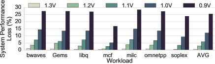
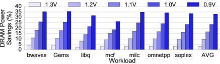
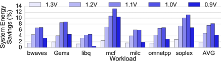
First, system performance loss increases as we lower , due to the increased DRAM access latency. However, different workloads experience a different rate of performance loss, as they tolerate memory latency differently. Among the memory-intensive workloads, mcf exhibits the lowest performance degradation since it has the highest memory intensity and high memory-level parallelism, leading to high queuing delays in the memory controller. The queuing delays and memory-level parallelism hide the longer DRAM access latency more than in other workloads. Other workloads lose more performance because they are less able to tolerate/hide the increased latency. Therefore, workloads with very high memory intensity and memory-level parallelism can be less sensitive to the increased memory latency.
Second, DRAM power savings increase with lower since reducing the DRAM array voltage decreases both the dynamic and static power components of DRAM. However, system energy savings does not monotonically increase with lower . We find that using =0.9V provides lower system energy savings than using =1.0V, as the processor takes much longer to run the applications at =0.9V. In this case, the increase in static DRAM and CPU energy outweighs the dynamic DRAM energy savings.
Third, reducing leads to a system energy reduction only when the reduction in DRAM energy outweighs the increase in CPU energy (due to the longer execution time). For =1.1V, the system energy reduces by an average of 7.6%. Therefore, we conclude that array voltage scaling is an effective technique that improves system energy consumption, with a small performance loss, for memory-intensive workloads.
Non-Memory-Intensive Workloads. Table 7.5 summarizes the system performance loss and energy savings of 20 non-memory-intensive workloads as varies from 1.30V to 0.90V, over the performance and energy consumption under a nominal of 1.35V. Compared to the memory-intensive workloads, non-memory-intensive workloads obtain smaller system energy savings, as the system energy is dominated by the processor. Although the workloads are more compute-intensive, lowering does reduce their system energy consumption, by decreasing the energy consumption of DRAM. For example, at 1.2V, array voltage scaling achieves an overall system energy savings of 2.5% with a performance loss of only 1.4%.
| 1.3V | 1.2V | 1.1V | 1.0V | 0.9V | |
|---|---|---|---|---|---|
| System Performance Loss (%) | 0.5 | 1.4 | 3.5 | 7.1 | 14.2 |
| DRAM Power Savings (%) | 3.4 | 10.4 | 16.5 | 22.7 | 29.0 |
| System Energy Savings (%) | 0.8 | 2.5 | 3.5 | 4.0 | 2.9 |
7.5.3 Effect of Performance-Aware Voltage Control
In this section, we evaluate the effectiveness of our complete proposal for Voltron, which incorporates our performance-aware voltage control mechanism to drive the array voltage scaling component intelligently. The performance-aware voltage control mechanism selects the lowest voltage level that satisfies the performance loss bound (provided by the user or system designer) based on our performance model (see Section 7.4.2). We evaluate Voltron with a target performance loss of 5%. Voltron executes the performance-aware voltage control mechanism once every four million cycles.888We evaluate the sensitivity to the frequency at which we execute the mechanism (i.e., the interval length of Voltron) in Section 7.5.8. We quantitatively compare Voltron to MemDVFS, a dynamic DRAM frequency and voltage scaling mechanism proposed by prior work [72], which we describe in Section 7.1.2. Similar to the configuration used in the prior work, we enable MemDVFS to switch dynamically between three frequency steps: 1600, 1333, and 1066 MT/s, which employ supply voltages of 1.35V, 1.3V, and 1.25V, respectively.
Figure 7.13 shows the system performance (WS) loss, DRAM power savings, and system energy savings due to MemDVFS and Voltron, compared to a baseline DRAM with a supply voltage of 1.35V. We show one graph per metric, where each graph uses boxplots to show the distribution among all workloads. In each graph, we categorize the workloads as either non-memory-intensive or memory-intensive. Each box illustrates the quartiles of the population, and the whiskers indicate the minimum and maximum values. The red dot indicates the mean. We make four major observations.
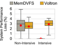
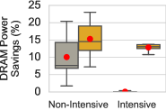
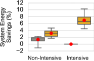
First, as shown in Figure 7.13(a), Voltron consistently selects a value that satisfies the performance loss bound of 5% across all workloads. Voltron incurs an average (maximum) performance loss of 2.5% (4.4%) and 2.9% (4.1%) for non-memory-intensive and memory-intensive workloads, respectively. This demonstrates that our performance model enables Voltron to select a low voltage value that saves energy while bounding performance loss based on the user’s requirement. We evaluate Voltron with a range of different performance targets in Section 7.5.7.
Second, MemDVFS has almost zero effect on memory-intensive workloads. This is because MemDVFS avoids scaling DRAM frequency (and hence voltage) when an application’s memory bandwidth utilization is above a fixed threshold. Reducing the frequency can result in a large performance loss since the memory-intensive workloads require high data throughput. As memory-intensive applications have high memory bandwidth consumption that easily exceeds the fixed threshold used by MemDVFS, MemDVFS cannot perform frequency and voltage scaling during most of the execution time. These results are consistent with the results reported in MemDVFS [72]. In contrast, Voltron reduces system energy (shown in Figure 7.13(c)) by 7.0% on average for memory-intensive workloads, at the cost of 2.9% system performance loss, which is well within the specified performance loss target of 5% (shown in Figure 7.13(a)).
Third, both MemDVFS and Voltron reduce the average system energy consumption for non-memory-intensive workloads. MemDVFS reduces system energy by dynamically scaling the frequency and voltage of DRAM, which lowers the DRAM power consumption (as shown in Figure 7.13(b)). By reducing the DRAM array voltage to a lower value than MemDVFS, Voltron is able to provide a slightly higher DRAM power and system energy reduction for non-memory-intensive workloads than MemDVFS.
Fourth, although Voltron reduces the system energy with a small performance loss, the average system energy efficiency, in terms of performance per watt (not shown in the figure), still improves by 3.3% and 7.4% for non-memory-intensive and memory-intensive workloads, respectively, over the baseline. Thus, we demonstrate that Voltron is an effective mechanism that improves system energy efficiency not only on non-memory-intensive applications, but also (especially) on memory-intensive workloads where prior work was unable to do so.
To summarize, across non-memory-intensive and memory-intensive workloads, Voltron reduces the average system energy consumption by 3.2% and 7.0% while limiting average system performance loss to only 2.5% and 2.9%, respectively. Voltron ensures that no workload loses performance by more than the specified target of 5%. We conclude that Voltron is an effective DRAM and system energy reduction mechanism that significantly outperforms prior memory DVFS mechanisms.
7.5.4 System Energy Breakdown
To demonstrate the source of energy savings from Voltron, Figure 7.14 compares the system energy breakdown of Voltron to the baseline, which operates at the nominal voltage level of 1.35V. The breakdown shows the average CPU and DRAM energy consumption across workloads, which are categorized into non-memory-intensive and memory-intensive workloads. We make two observations from the figure.
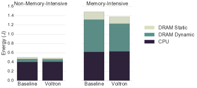
First, in the non-memory-intensive workloads, the CPU consumes an average of 80% of the total system energy when the DRAM uses the nominal voltage level. As a result, Voltron has less potential to reduce the overall system energy as it reduces only the DRAM energy, which makes up only 20% of the total system energy. Second, DRAM consumes an average of 53% of the total system energy in the memory-intensive workloads. As a result, Voltron has a larger room for potential improvement for memory-intensive workloads than for non-memory-intensive workloads. Across the memory-intensive workloads, Voltron reduces the average dynamic and static DRAM energy by 14% and 11%, respectively. However, Voltron increases the CPU energy consumption by 1.7%, because the application incurs a small system performance degradation (due to the increased memory access latency), which is within our 5% performance loss target (as shown in Section 7.5.3). We conclude that Voltron is effective in reducing DRAM energy, and it is an effective system energy reduction mechanism, especially when DRAM is a major consumer of energy in the system.
7.5.5 Effect of Exploiting Spatial Locality of Errors
In Section 7.3.3, our experimental results show that errors due to reduced voltage concentrate in certain regions, specifically in select DRAM banks for some vendors’ DIMMs. This implies that when we lower the voltage, only the banks with errors require a higher access latency to read or write data correctly, whereas error-free banks can be accessed reliably with the standard latency. Therefore, in this section, we enhance our Voltron mechanism by exploiting the spatial locality of errors caused by reduced-voltage operations. The key idea is to dynamically change the access latency on a per-bank basis (i.e., based on the DRAM banks being accessed) to account for the reliability of each bank. In other words, we would like to increase the latency only for banks that would otherwise experience errors, and do so just enough such that these banks operate reliably.
For our evaluation, we model the behavior based on a subset (three) of Vendor C’s DIMMs, which show that the number of banks with errors increases as we reduce the supply voltage (Section 7.3.3). We observe that these DIMMs start experiencing errors at 1.1V using the standard latency values. However, only one bank observes errors when we reduce the voltage level from 1.15V to 1.1V (i.e., 50mV reduction). We evaluate a conservative model that increases the number of banks that need higher latency by one for every 50mV reduction from the nominal voltage of 1.35V. Note that this model is conservative, because we start increasing the latency when the voltage is reduced to 1.3V, which is much higher than the lowest voltage level (1.15V) for which we observe that DIMMs operate reliably without requiring a latency increase. Based on this conservative model, we choose the banks whose latencies should increase sequentially starting from the first bank, while the remaining banks operate at the standard latency. For example, at 1.25V (100mV lower than the nominal voltage of 1.35V), Voltron needs to increase the latency for the first two out of the eight banks to ensure reliable operation.
Figure 7.15(a) compares the system performance and energy efficiency of our bank-error locality aware version of Voltron (denoted as Voltron+BL) to the previously-evaluated Voltron mechanism, which is not aware of such locality. By increasing the memory latency for only a subset of banks at each voltage step, Voltron+BL reduces the average performance loss from 2.9% to 1.8% and increases the average system energy savings from 7.0% to 7.3% for memory-intensive workloads, with similar improvements for non-memory-intensive workloads. We show that enhancing Voltron by adding awareness of the spatial locality of errors can further mitigate the latency penalty due to reduced voltage, even with the conservative bank error locality model we assume and evaluate in this example. We believe that a mechanism that exploits spatial error locality at a finer granularity could lead to even higher performance and energy savings, but we leave such an evaluation to future work.
[0.49]
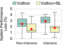 [0.49]
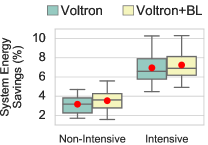
7.5.6 Effect on Heterogeneous Workloads
So far, we have evaluated Voltron on homogeneous multi-core workloads, where each workload consists of the same benchmark running on all cores. In this section, we evaluate the effect of Voltron on heterogeneous workloads, where each workload consists of different benchmarks running on each core. We categorize the workloads based on the fraction of memory-intensive benchmarks in the workload (0%, 25%, 50%, 75%, and 100%). Each category consists of 10 workloads, resulting in a total of 50 workloads across all categories.
Figure 7.16 shows the system performance loss and energy efficiency improvement (in terms of performance per watt) with Voltron and with MemDVFS for heterogeneous workloads. The error bars indicate the 95% confidence interval across all workloads in the category. We make two observations from the figure. First, for each category of the heterogeneous workloads, Voltron is able to meet the 5% performance loss target on average. However, since Voltron is not designed to provide a hard performance guarantee for every single workload, Voltron exceeds the performance loss target for 10 out of the 50 workloads, though it exceeds the target by only 0.76% on average. Second, the energy efficiency improvement due to Voltron becomes larger as the memory intensity of the workload increases. This is because the fraction of system energy coming from memory grows with higher memory intensity, due to the higher amount of memory traffic. Therefore, the memory energy reduction from Voltron has a greater impact at the system level with more memory-intensive workloads. On the other hand, MemDVFS becomes less effective with higher memory intensity, as the memory bandwidth utilization more frequently exceeds the fixed threshold employed by MemDVFS. Thus, MemDVFS has a smaller opportunity to scale the frequency and voltage. We conclude that Voltron is an effective mechanism that can adapt to different applications’ characteristics to improve system energy efficiency.
[0.49]
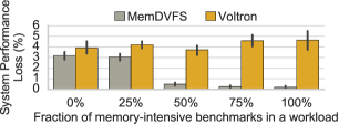 [0.49]
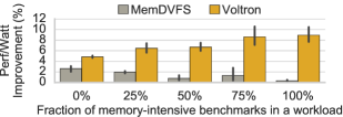
7.5.7 Effect of Varying the Performance Target
Figure 7.17(a) shows the performance loss and energy efficiency improvement due to Voltron as we vary the system performance loss target for both homogeneous and heterogeneous workloads. For each target, we use a boxplot to show the distribution across all workloads. In total, we evaluate Voltron on 1001 combinations of workloads and performance targets: 27 homogeneous workloads 13 targets + 50 heterogeneous workloads 13 targets. The first major observation is that Voltron’s performance-aware voltage control mechanism adapts to different performance targets by dynamically selecting different voltage values at runtime. Across all 1001 runs, Voltron keeps performance within the performance loss target for 84.5% of them. Even though Voltron cannot enforce a hard performance guarantee for all workloads, it exceeds the target by only 0.68% on average for those workloads where it does not strictly meet the target.
[][c]
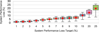 [][c]
[][c]
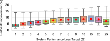
Second, system energy efficiency increases with higher performance loss targets, but the gains plateau at around a target of 10%. Beyond the 10% target, Voltron starts selecting smaller values (e.g., 0.9V) that result in much higher memory latency, which in turn increases both the CPU runtime and system energy. In Section 7.5.2, we observed that employing a value less than 1.0V can result in smaller system energy savings than using =1.0V.
We conclude that, compared to prior work on memory DVFS, Voltron is a more flexible mechanism, as it allows the users or system designers to select a performance and energy trade-off that best suits their target system or applications.
7.5.8 Sensitivity to the Profile Interval Length
Figure 7.18 shows the average system energy efficiency improvement due to Voltron with different profile interval lengths measured across 27 homogeneous workloads. As the profile interval length increases beyond two million cycles, we observe that the energy efficiency benefit of Voltron starts reducing. This is because longer intervals prevent Voltron from making faster adjustments based on the collected new profile information. Nonetheless, Voltron consistently improves system energy efficiency for all evaluated profile interval lengths.
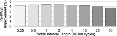
7.6 Summary
In this chapter, we provide the first experimental study that comprehensively characterizes and analyzes the behavior of DRAM chips when the supply voltage is reduced below its nominal value. We demonstrate, using 124 DDR3L DRAM chips, that the DRAM supply voltage can be reliably reduced to a certain level, beyond which errors arise within the data. We then experimentally demonstrate the relationship between the supply voltage and the latency of the fundamental DRAM operations (activation, restoration, and precharge). We show that bit errors caused by reduced-voltage operation can be eliminated by increasing the latency of the three fundamental DRAM operations. By changing the memory controller configuration to allow for the longer latency of these operations, we can thus further lower the supply voltage without inducing errors in the data. We also experimentally characterize the relationship between reduced supply voltage and error locations, stored data patterns, temperature, and data retention.
Based on these observations, we propose and evaluate Voltron, a low-cost energy reduction mechanism that reduces DRAM energy without affecting memory data throughput. Voltron reduces the supply voltage for only the DRAM array, while maintaining the nominal voltage for the peripheral circuitry to continue operating the memory channel at a high frequency. Voltron uses a new piecewise linear performance model to find the array supply voltage that maximizes the system energy reduction within a given performance loss target. Our experimental evaluations across a wide variety of workloads demonstrate that Voltron significantly reduces system energy consumption with only very modest performance loss.
Appendix
Appendix 7.A FPGA Schematic of DRAM Power Pins
Figure 7.A.1 shows a schematic of the DRAM pins that our FPGA board [364] connects to (see Section 7.2 for our experimental methodology). Since there are a large number of pins that are used for different purposes (e.g., data address), we zoom in on the right side of the figure to focus on the power pins that we adjust for our experiments in this chapter. Power pin numbering information can be found on the datasheets provided by all major vendors (e.g., [236, 316, 296]). In particular, we tune the VCC1V5 pin on the FPGA, which is directly connected to all of the and pins on the DIMM. The reference voltage VTTVREF is automatically adjusted by the DRAM to half of VCC1V5.
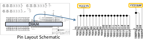
Appendix 7.B Effect of Data Pattern on Error Rate
As discussed in Section 7.3.1, we do not observe a significant effect of different stored data patterns on the DRAM error rate when we reduce the supply voltage. Figure 7.B.1 shows the average bit error rate (BER) of three different data patterns (aa, cc, and ff) across different supply voltage levels for each vendor. Each data pattern represents the byte value (shown in hex) that we fill into the DRAM. The error bars indicate the 95% confidence interval. We make two observations from the figure.
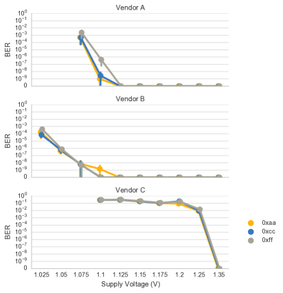
First, the BER increases as we reduce the supply voltage for all three data patterns. We made a similar observation in Section 7.3.1, which shows that the fraction of errors increases as the supply voltage drops. We explained our hypothesis on the cause of the errors, and used both experiments and simulations to test the hypothesis, in Section 7.3.2.
Second, we do not observe a significant difference across the BER values from the three different data patterns. We attempt to answer the following question: Do different data patterns induce BER values that are statistically different from each other at each voltage level? To answer this, we conduct a one-way ANOVA (analysis of variance) test across the measured BERs from all three data patterns at each supply voltage level to calculate a p-value. If the p-value is below 0.05, we can claim that these three data patterns induce a statistically-significant difference on the error rate. Table 7.B.1 shows the calculated p-value at each supply voltage level. At certain supply voltage levels, we do not have a p-value listed (shown as — or in the table), either because there are no errors (indicated as —) or we cannot reliably access data from the DIMMs even if the access latency is higher than the standard value (indicated as ).
| Supply | Vendor | ||
|---|---|---|---|
| Voltage | A | B | C |
| 1.305 | — | — | — |
| 1.250 | — | — | 0.000000 |
| 1.200 | — | — | 0.029947 |
| 1.175 | — | — | 0.856793 |
| 1.150 | — | — | 0.872205 |
| 1.125 | — | 0.375906 | 0.897489 |
| 1.100 | 0.028592 | 0.375906 | 0.000000 |
| 1.075 | 0.103073 | 0.907960 | |
| 1.050 | 0.651482 | ||
| 1.025 | 0.025167 | ||
Using the one-way ANOVA test, we find that using different data patterns does not have a statistically significant (i.e., p-value 0.05) effect on the error rate at all supply voltage levels. Significant effects (i.e., p-value 0.05) occur at 1.100V for Vendor A, at 1.025V for Vendor B, and at both 1.250V and 1.100V for Vendor C. As a result, our study does not provide enough evidence to conclude that using any of the three data patterns (aa, cc, and ff) induces higher or lower error rates than the other two patterns at reduced voltage levels.
Appendix 7.C SPICE Simulation Model
We perform circuit-level SPICE simulations to understand in detail how the DRAM cell arrays operate at low supply voltage. We model a DRAM cell array in SPICE, and simulate its behavior for different supply voltages. We have released our SPICE model online [2].
DRAM Cell Array Model. We build a detailed cell array model, as shown in Figure 7.C.1. In the cell array, the DRAM cells are organized as array, which is a common organization in modern DRAM chips [357]. Each column is vertical, and corresponds to 512 cells sharing a bitline that connects to a sense amplifier. Due to the bitline wire and the cells that are connected to the bitline, there is parasitic resistance and capacitance on each bitline. Each row consists of 512 cells sharing the same wordline, which also has parasitic resistance and capacitance. The amount of parasitic resistance and capacitance on the bitlines and wordlines is a major factor that affects the latency of DRAM operations accessing a cell array [193, 190].
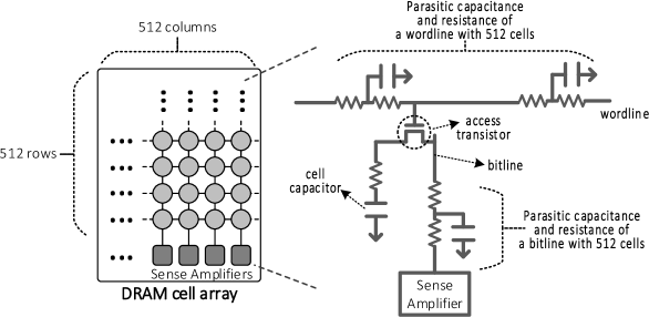
Simulation Methodology. We use the LTspice [207] SPICE simulator to perform our simulations. To find the access latency of the DRAM operations under different supply voltages, we build a DRAM cell array using technology parameters that we derive from a DRAM model [357] and from a process technology model [282, 378]. By default, we assume that the cell capacitance is and the bitline capacitance is [357]. The nominal is 1.35V, and we perform simulations to obtain the latency of DRAM operations at every 25mV step from 1.35V down to 0.9V. The results of our SPICE simulations are discussed in Section 7.3.1 and 7.3.2.
Appendix 7.D Spatial Distribution of Errors
In this section, we expand upon the spatial locality data presented in Section 7.3.3. Figures 7.D.1, 7.D.2, and 7.D.3 show the physical locations of errors that occur when the supply voltage is reduced for a representative DIMM from Vendors A, B, and C, respectively. At higher voltage levels, even if errors occur, they tend to cluster in certain regions of a DIMM. However, as we reduce the supply voltage further, the number of errors increases, and the errors start to spread across the entire DIMM.

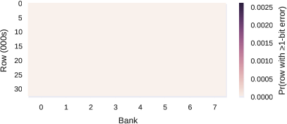
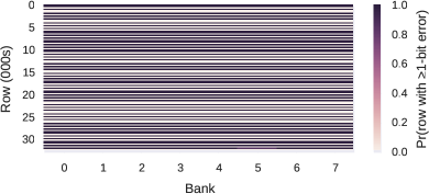
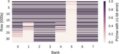
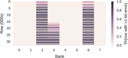
Appendix 7.E Full Information of Every Tested DIMM
Table 7.E lists the parameters of every DRAM module that we evaluate, along with the we discovered for each module based on our experimental characterization (Section 7.3.1). We provide all results for all DIMMs in our GitHub repository [2].
| Vendor | Module | Date∗ | Timing† | Organization | Chip | |||||||
| (yy-ww) | Freq (MT/s) | tRCD (ns) | tRP (ns) | tRAS (ns) | Size (GB)‡ | Chips⋆ | Size (Gb) | Pins | Die Version§ | Vmin (V)∘ | ||
| A | 15-46 | 1600 | 13.75 | 13.75 | 35 | 2 | 4 | 4 | 16 | 1.100 | ||
| A | 15-47 | 1600 | 13.75 | 13.75 | 35 | 2 | 4 | 4 | 16 | 1.125 | ||
| A | 15-44 | 1600 | 13.75 | 13.75 | 35 | 2 | 4 | 4 | 16 | 1.125 | ||
| A | 16-01 | 1600 | 13.75 | 13.75 | 35 | 2 | 4 | 4 | 16 | 1.125 | ||
| A | 16-01 | 1600 | 13.75 | 13.75 | 35 | 2 | 4 | 4 | 16 | 1.125 | ||
| A | 16-10 | 1600 | 13.75 | 13.75 | 35 | 2 | 4 | 4 | 16 | 1.125 | ||
| A | 16-12 | 1600 | 13.75 | 13.75 | 35 | 2 | 4 | 4 | 16 | 1.125 | ||
| A | 16-09 | 1600 | 13.75 | 13.75 | 35 | 2 | 4 | 4 | 16 | 1.125 | ||
| A | 16-11 | 1600 | 13.75 | 13.75 | 35 | 2 | 4 | 4 | 16 | 1.100 | ||
| A Total of 10 DIMMs | A | 16-10 | 1600 | 13.75 | 13.75 | 35 | 2 | 4 | 4 | 16 | 1.125 | |
| B | 14-34 | 1600 | 13.75 | 13.75 | 35 | 2 | 4 | 4 | 16 | 1.100 | ||
| B | 14-34 | 1600 | 13.75 | 13.75 | 35 | 2 | 4 | 4 | 16 | 1.150 | ||
| B | 14-26 | 1600 | 13.75 | 13.75 | 35 | 2 | 4 | 4 | 16 | 1.100 | ||
| B | 14-30 | 1600 | 13.75 | 13.75 | 35 | 2 | 4 | 4 | 16 | 1.100 | ||
| B | 14-34 | 1600 | 13.75 | 13.75 | 35 | 2 | 4 | 4 | 16 | 1.125 | ||
| B | 14-32 | 1600 | 13.75 | 13.75 | 35 | 2 | 4 | 4 | 16 | 1.125 | ||
| B | 14-34 | 1600 | 13.75 | 13.75 | 35 | 2 | 4 | 4 | 16 | 1.100 | ||
| B | 14-30 | 1600 | 13.75 | 13.75 | 35 | 2 | 4 | 4 | 16 | 1.125 | ||
| B | 14-23 | 1600 | 13.75 | 13.75 | 35 | 2 | 4 | 4 | 16 | 1.125 | ||
| B | 14-21 | 1600 | 13.75 | 13.75 | 35 | 2 | 4 | 4 | 16 | 1.125 | ||
| B | 14-31 | 1600 | 13.75 | 13.75 | 35 | 2 | 4 | 4 | 16 | 1.100 | ||
| B Total of 12 DIMMs | B | 15-08 | 1600 | 13.75 | 13.75 | 35 | 2 | 4 | 4 | 16 | 1.100 | |
| C | 15-33 | 1600 | 13.75 | 13.75 | 35 | 2 | 4 | 4 | 16 | 1.300 | ||
| C | 15-33 | 1600 | 13.75 | 13.75 | 35 | 2 | 4 | 4 | 16 | 1.250 | ||
| C | 15-33 | 1600 | 13.75 | 13.75 | 35 | 2 | 4 | 4 | 16 | 1.150 | ||
| C | 15-33 | 1600 | 13.75 | 13.75 | 35 | 2 | 4 | 4 | 16 | 1.150 | ||
| C | 15-33 | 1600 | 13.75 | 13.75 | 35 | 2 | 4 | 4 | 16 | 1.300 | ||
| C | 15-33 | 1600 | 13.75 | 13.75 | 35 | 2 | 4 | 4 | 16 | 1.300 | ||
| C | 15-33 | 1600 | 13.75 | 13.75 | 35 | 2 | 4 | 4 | 16 | 1.300 | ||
| C | 15-33 | 1600 | 13.75 | 13.75 | 35 | 2 | 4 | 4 | 16 | 1.250 | ||
| C Total of 9 DIMMs | C | 15-33 | 1600 | 13.75 | 13.75 | 35 | 2 | 4 | 4 | 16 | 1.300 | |
| The manufacturing date in the format of year-week (yy-ww). For example, 15-01 indicates that the DIMM |
| was manufactured during the first week of 2015. |
| The timing factors associated with each DIMM: |
| : the channel frequency |
| : the minimum required latency for an activate to complete |
| : the minimum required latency for a Phys. Rev. Eto complete |
| : the minimum required latency for to restore the charge in an activated row of cells |
| The maximum DRAM module size supported by our testing platform is 2GB. |
| The number of DRAM chips mounted on each DRAM module. |
| The DRAM die versions that are marked on the chip package. |
| The minimum voltage level that allows error-free operation, as described in Section 7.3.1. |
Chapter 8 Conclusions and Future Directions
Over the past few decades, long DRAM access latency has been a critical bottleneck in system performance. Increasing core counts and the emergence of increasingly more data-intensive and latency-critical applications further exacerbate the performance penalty of high memory latency. Therefore, providing low-latency memory accesses is more critical now than ever before for achieving high system performance. While certain specialized DRAM architectures provide low memory latency, they come at a high cost (e.g., 39x higher than the common DDRx DRAM chips, as described in Chapter 1) with low chip density. As a result, the goal of this dissertation is to enable low-latency DRAM-based memory systems at low cost, with a solid understanding of the latency behavior in DRAM based on experimental characterization on real DRAM chips.
To this end, we propose a series of mechanisms to reduce DRAM access latency at low cost. First, we propose Lost-Cost Inter-Linked Subarrays (LISA) to enable low-latency, high-bandwidth inter-subarray connectivity within each bank at a very modest cost of 0.8% DRAM area overhead. Using this new inter-subarray connection, DRAM can perform inter-subarray data movement at 26x the bandwidth of a modern 64-bit DDR4-2400 memory channel. We exploit LISA’s fast inter-subarray movement to propose three new architectural mechanisms that reduce the latency of two frequently-used system API calls (i.e., memcpy and memmove) and the three fundamental DRAM operations, i.e., activation, restoration, and precharge. We describe and evaluate three such mechanisms in this dissertation: (1) Rapid Inter-Subarray Copy (RISC), which copies data across subarrays at low latency and low DRAM energy; (2) Variable Latency (VILLA) DRAM, which reduces the access latency of frequently-accessed data by caching it in fast subarrays; and (3) Linked Precharge (LIP), which reduces the precharge latency for a subarray by linking its precharge units with neighboring idle precharge units. Our evaluations show that the three new mechanisms of LISA significantly improve system performance and energy efficiency when used individually or together, across a variety of workloads and system configurations.
Second, we mitigate the refresh interference, which incurs long memory latency, by proposing two access-refresh parallelization mechanisms that enable overlapping more accesses with refreshes inside DRAM. These two refresh mechanisms are 1) DARP, a new per-bank refresh scheduling policy that proactively schedules refreshes to banks that are idle or that are draining writes and 2) SARP, a refresh architecture that enables a bank to serve memory requests in idle subarrays while other subarrays are being refreshed. DARP introduces minor modifications to only the memory controller, and SARP incurs a very modest cost of 0.7% DRAM area overhead. Our extensive evaluations on a wide variety of systems and workloads show that these two mechanisms significantly improve system performance and outperform state-of-the-art refresh policies. These two techniques together achieve performance close to an idealized system that does not require refresh.
Third, this dissertation provides the first experimental study that comprehensively characterizes and analyzes the latency variation within modern DRAM chips for three fundamental DRAM operations (activation, precharge, and restoration). We experimentally demonstrate that significant variation is present across DRAM cells within our tested DRAM chips. Based on our experimental characterization, we propose a new mechanism, FLY-DRAM, which exploits the lower latencies of DRAM regions with faster cells by introducing heterogeneous timing parameters into the memory controller. We demonstrate that FLY-DRAM can greatly reduce DRAM latency, leading to significant system performance improvements on a variety of workloads.
Finally, for the first time, we perform detailed experimental characterization that studies the critical relationship between DRAM supply voltage and DRAM access latency in modern DRAM chips. Our detailed characterization of real commodity DRAM chips demonstrates that memory access latency reduces with increasing supply voltage. Based on our characterization, we propose Voltron, a new mechanism that improves system energy efficiency by dynamically adjusting the DRAM supply voltage based on a performance model.
8.1 Summary of Latency Reduction
In this section, we summarize the memory latency reduction due to mechanisms proposed in this dissertation. In the particular systems that we evaluated in this dissertation, a last-level cache (LLC) miss generates a DRAM request that requires multiple fundamental DRAM operations (e.g., activation, restoration, precharge). Our mechanisms focus on improving the latency of these fundamental DRAM operations after an LLC miss. Note that our proposals can potentially be applied to different memory technologies in the memory hierarchy, such as eDRAM (which typically serves as an LLC), providing additional latency benefits.
Specifically, DRAM has five major timing parameters associated with the DRAM operations that are used to access a cache line in a closed row: tRCD, tRAS, tCL, tBL, and tRP, which are shown in Figure 8.1.1. Since we have already explained the details of these timing parameters in Chapter 2, we focus on summarizing the improvements on these timing parameters due to our proposed techniques in this section.
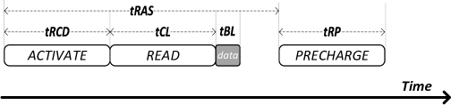
In this dissertation, our proposals reduce three of the five timing parameters: tRCD, tRAS, and tRP. These three timing parameters are crucial for systems that generate a large number of random accesses (e.g., reading buffered network packets) or data dependent accesses (e.g., pointer chasing). Since the read timing parameter (tCL) is a DRAM-internal timing that is determined by a clock inside DRAM, our testing platform does not have the capability to characterize its behavior. We leave the study on tCL to future work. On the other hand, tBL is determined by the width and frequency of the DRAM channel, which is not the focus of this dissertation. In addition to addressing the three major DRAM timing parameters, our dissertation also reduces the bulk copy latency and the refresh-induced latency. Table 8.1.1 lists the quantitative latency improvements due to each of our proposed mechanisms for the high-density DDRx DRAM chips.
| Mechanisms | Improved Latency Components | Latency (ns) | Improvement |
|---|---|---|---|
| LISA-RISC (§4.4) | Copy latency of 4KB data | 148.5 | 9.2x |
| LISA-VILLA (§4.5) | tRCD/tRAS/tRP | 7.5/13/8.5 | 1.8x/2.7x/1.5x |
| LISA-LIP (§4.6) | tRP | 5 | 2.6x |
| FLY-DRAM (§6.6.1) | tRCD/tRAS/tRP | 7.5/27/7.5 | 1.8x/1.3x/1.8x |
| DSARP (§5.2) | Avg. latency of read requests | 199/200/202 | 1.2x/1.3x/1.5x |
| for 8/16/32Gb DRAM chips |
The three mechanisms built on top of LISA reduce various latency components. First, Rapid Inter-Subarray Copy (RISC) significantly reduces the bulk copy latency between subarrays by 9.2x. Second, Variable Latency (VILLA) DRAM reduces the access latency (i.e., tRCD, tRAS, and tRP) of frequently-accessed data by caching it in fast subarrays with shorter bitlines. Third, LIP reduces the precharge latency of every subarray by 2.6x. LIP connects two precharge units of adjacent subarrays together using LISA to accelerate the precharge operation. In total, the three LISA mechanisms together incur a small DRAM chip area overhead of 2.4%.
Flexible-Latency (FLY) DRAM reduces the three major timing parameters by exploiting our experimental observation on latency variation within commodity DDR3 DRAM chips. The key idea of FLY-DRAM is to determine the shortest reliable access latency of each DRAM region, and to use the memory controller to apply that latency to the corresponding DRAM region at runtime. Overall, FLY-DRAM reduces the latency of tRCD/tRAS/tRP by 1.8x/1.3x/1.8x for accesses to those DRAM regions without slow cells. FLY-DRAM does not require any modification to the DRAM chips since it leverages the innate latency behavior that varies across DRAM cells within the same DRAM chip.
To address the refresh-induced latency, DSARP mitigates refresh latency by parallelizing refresh operations with memory accesses within the DRAM chip. As a result, DSARP reduces the average latency of read requests across 100 different 8-core workloads by 1.2x/1.3x/1.5x for 8/16/32Gb DRAM chips. DSARP incurs a low DRAM chip area overhead of 0.7%.
We conclude that our dissertation enables significant latency improvements at very low cost in high-density DRAM chips by augmenting DRAM architecture with simple and low-cost features, and developing a better understanding of manufactured DRAM chips.
8.2 Future Research Directions
This dissertation opens up several avenues of future research directions. In this section, we describe several directions that can tackle other problems related to memory systems based on the ideas and approaches proposed in this dissertation.
8.2.1 Enabling LISA to Perform 1-to-N Memory Copy or Move Operations
A typical memcpy or memmove call only allows the data to be copied from one source location to one destination location. To copy or move data from one source location to multiple different destinations, repeated calls are required. The problem is that such repeated calls incur long latency and high bandwidth consumption. In Chapter 4, we propose to use the LISA substrate to accelerate memcpy and memmove in DRAM without the intervention of CPU. One potential application that can be enabled by LISA is performing memcpy or memmove from one source location to multiple destinations completely in DRAM without requiring multiple calls of these operations.
By using LISA, we observe that moving data from the source subarray to the destination subarray latches the source row’s data in all the intermediate subarrays’ row buffer. As a result, activating these intermediate subarrays would copy their row buffers’ data into the specified row. By extending LISA to perform multi-point (1-to-N) copy or move operations, we can significantly increase system performance of several commonly-used system operations. For example, forking multiple child processes can utilize 1-to-N copy operations to copy those memory regions that are likely to be modified by the children.
8.2.2 In-Memory Computation with LISA
One important requirement of efficient in-memory computation is being able to move data from its stored location to the computation units with very low latency and energy. In Chapter 4, we discussed the benefits of using LISA to extend the data range of in-memory bitwise operations. We believe using the LISA substrate can enable a new in-memory computation framework. The idea is to add a small computation unit inside each or a subset of banks, and connect these computation units to the neighboring subarrays which store the data. Doing so allows the system to utilize LISA to move bulk data from the subarrays to the computation under low latency with low area overhead.
Two potential types of computation units to add are bitwise shifters and ripple-carry adders since simple integer addition and bitwise shifting between two arrays of data are common operations in many applications. One key challenge of adding computation units would be fitting each single unit that processes a single bit within a pitch of DRAM array’s column. For example, a single-bit shifter requires 12 transistors which is much bigger than a sense amplifier (4 transistors). This implementation overhead can restrict the computation to process data at the granularity of a row size. Nonetheless, this general in-memory computation framework still has the potential to enable simple filtering operations in memory to provide high system performance or energy efficiency at low cost.
8.2.3 Extending LISA to Non-Volatile Memory
In this dissertation, we only focus on the DRAM technology. A class of emerging memory technology is non-volatile memory (NVM), which has the capability of retaining data without power supply. We believe that the LISA substrate can be extended to NVM (e.g., STT-RAM) since the memory organization of NVM mostly resembles that of DRAM. A potential application of LISA in NVM is an efficient file copy operation that does not incur costly I/O data transfer.
8.2.4 Data Prefetching with Variable Latency (VILLA) DRAM
Data prefetching utilizes unused memory bandwidth to speculatively transfer data from memory to caches. However, if memory bandwidth is heavily utilized, prefetch requests can degrade system performance by interfering with demand requests. Therefore, a prefetching scheme that does not exert pressure on memory channels can potentially attain higher system performance.
In Section 4.5, we described a new heterogeneous DRAM design, called Variable Latency (VILLA) DRAM, which introduces fast subarrays in each DRAM bank. VILLA utilizes the LISA substrate to efficiently transfer row-size data (8KB) from a slow subarray to a fast subarray without using the memory channel. We believe a new prefetching scheme can be designed with the VILLA cache by prefetching a whole row of data before demand requests occur. The primary benefit is that prefetching to VILLA cache does not cause bandwidth contention. Also, VILLA can increase the prefetch coverage since the prefetching granularity is large, with hundreds of cache lines.
8.2.5 Reducing Activation Latency with Error Detection Codes
In Chapter 6, we observed that activation errors (due to reduced activation latency) are permanent by propagating back into the first accessed column of data. If the errors were transient, a new mechanism could be devised to read data with aggressively-reduced activation latency and re-read data when activation errors occur. Activation errors can be detected using error detection codes. Therefore, this raises a key question: can we modify the DRAM sensing circuit to make activation errors transient? Answering this question requires a thorough understanding of the modern DRAM circuit to find out how activation errors propagate back into DRAM cells.
8.2.6 Characterizing Latency Behavior of DRAM Cells Over Time
In Chapter 6, we experimentally demonstrated that individual cells within the same DRAM chip exhibit different latency behavior. However, we do not examine the latency behavior of each cell over a controlled period of time, except for the fact that we perform the tests for multiple rounds per DIMM. The latency of a cell could potentially change over time, within a short period of time (e.g., similar effect as Variable Retention Time) or long period of time (e.g., aging and wearout). Therefore, a future direction is to experimentally study the latency behavior of DRAM cells over time.
8.2.7 Avoiding Worst-Case Data Patterns for Higher Reliability
Our experimental characterization in Section 6.3 showed that errors caused by reduced activation latency are dependent on the stored data pattern. Reading bit 1 is significantly more reliable than bit 0 at reduced activation latencies. To improve reliability of future DRAM, a future research direction is to design new encoding scheme that will (1) increase the number of bit 1 and (2) store the encoding metadata at low cost.
8.3 Final Concluding Remarks
In this dissertation, we highlighted problems that cause or affect long DRAM latency and presented extensive experimental characterization on studying DRAM latency behavior in commodity DRAM chips. Overall, we presented four new techniques: 1) LISA, which is a versatile DRAM substrate that provides fast data movement between subarrays to enable several low-latency mechanisms, 2) DSARP, which overlaps accesses with refreshes to reduce refresh-induced latency, 3) FLY-DRAM, which exploits our experimental characterization on latency variation within a chip to reduce latency to access regions with faster DRAM cells, and 4) Voltron, which exploits our experimental characterization on the critical relationship between access latency and supply voltage to improve energy efficiency. We conclude and hope the proposed low-latency architectural mechanisms and the detailed experimental characterization on commodity DRAM chips in this dissertation will pave the way for new research that can develop new mechanisms to improve system performance, energy efficiency, or reliability of future memory systems.
Other Works of the Author
Throughout the course of my Ph.D. study, I have worked on several different topics with many fellow graduate students from CMU and collaborators from other institutions. In this chapter, I would like to acknowledge these works.
In the early years of my Ph.D., I worked on a number of projects on networks-on-chip (NoCs). In collaboration with Rachata Ausavarungnirun, Chris Fallin, and others, we have contributed to a new congestion control algorithm (HAT [61]), a new router architecture (MinBD [88]), and a new hierarchical ring design (HiRD [19]). We show that these new techniques can significantly improve the energy efficiency of NoCs.
Another topic that I have developed an interest and worked on was memory scheduling policy for heterogeneous processors that consist of conventional CPU cores and other types of accelerators. In collaboration with Rachata Ausavarungnirun and Lavanya Subramanian, we have developed a new memory scheduler, SMS [18], that improves system performance and fairness of a CPU-GPU processor by reducing the application interference between CPU and GPU. I have also contributed to a memory scheduler that targets another type of heterogeneous processor that consists of conventional CPU cores and hardware accelerators for image processing and recognition. In collaboration with Hiroyuki Usui and Lavanya Subramanian, we have developed a memory scheduler, DASH [352], that enables the accelerators to meet their deadlines while attaining high system performance.
In collaboration with Hasan Hassan, I have worked on developing a DRAM-testing infrastructure, SoftMC [109], that has facilitated my research on DRAM characterization and other works. In collaboration with Donghyuk Lee, I have contributed to another low DRAM latency architecture, AL-DRAM [192], that adaptively adjusts latency of DRAM based on the ambient temperature.
Finally, we have released the simulators used for these different works on GitHub. The simulators that I contributed to are as follows: (1) NoCulator for NoCs evaluation, (2) Ramulator (in C and C#) for memory projects, and (3) SoftMC, which is an FPGA-based memory controller design, for DRAM characterization. The source code is available on GitHub at https://github.com/CMU-SAFARI.
References
- [1] Ramulator. https://github.com/CMU-SAFARI/ramulator, 2015.
- [2] DRAM Voltage Study. https://github.com/CMU-SAFARI/DRAM-Voltage-Study, 2017.
- [3] N. Agarwal, D. Nellans, M. Stephenson, M. O’Connor, and S. W. Keckler. Page Placement Strategies for GPUs Within Heterogeneous Memory Systems. In ASPLOS, 2015.
- [4] A. Agrawal, A. Ansari, and J. Torrellas. Mosaic: Exploiting the spatial locality of process variation to reduce refresh energy in on-chip eDRAM modules. In HPCA, 2014.
- [5] A. Agrawal et al. Refrint: Intelligent Refresh to Minimize Power in On-Chip Multiprocessor Cache Hierarchies. In HPCA, 2013.
- [6] A. Agrawal, M. O’Connor, E. Bolotin, N. Chatterjee, J. Emer, and S. Keckler. CLARA: Circular Linked-List Auto and Self Refresh Architecture. In MEMSYS, 2016.
- [7] J. Ahn, S. Hong, S. Yoo, O. Mutlu, and K. Choi. A scalable processing-in-memory accelerator for parallel graph processing. In ISCA, 2015.
- [8] J. Ahn, S. Yoo, O. Mutlu, and K. Choi. Pim-enabled instructions: A low-overhead, locality-aware processing-in-memory architecture. In ISCA, 2015.
- [9] J. H. Ahn, N. P. Jouppi, C. Kozyrakis, J. Leverich, and R. S. Schreiber. Improving System Energy Efficiency with Memory Rank Subsetting. TACO, 9(1):4:1–4:28, 2012.
- [10] J. H. Ahn, J. Leverich, R. Schreiber, and N. P. Jouppi. Multicore DIMM: an Energy Efficient Memory Module with Independently Controlled DRAMs. CAL, 2009.
- [11] A. Ailamaki, D. J. DeWitt, M. D. Hill, and D. A. Wood. DBMSs on a Modern Processor: Where Does Time Go? In VLDB, 1999.
- [12] B. Akin, F. Franchetti, and J. C. Hoe. Data Reorganization in Memory Using 3D-stacked DRAM. In ISCA, 2015.
- [13] Z. Al-Ars, S. Hamdioui, and G. Gaydadjiev. Manifestation of Precharge Faults in High Speed DRAM Devices. 2007.
- [14] Z. Al-Ars, S. Hamdioui, and A. J. van de Goor. Effects of bit line coupling on the faulty behavior of DRAMs. 2004.
- [15] A. R. Alameldeen and D. A. Wood. Interactions Between Compression and Prefetching in Chip Multiprocessors. In HPCA, 2007.
- [16] G. Appenzeller, I. Keslassy, and N. McKeown. Sizing Router Buffers. In SIGCOMM, 2004.
- [17] ARM Ltd. Cortex-A9 Processor. https://www.arm.com/products/processors/cortex-a/cortex-a9.php.
- [18] R. Ausavarungnirun, K. K.-W. Chang, L. Subramanian, G. H. Loh, and O. Mutlu. Staged memory scheduling: Achieving high performance and scalability in heterogeneous systems. In ISCA, 2012.
- [19] R. Ausavarungnirun, C. Fallin, X. Yu, K. K. W. Chang, G. Nazario, R. Das, G. H. Loh, and O. Mutlu. Design and evaluation of hierarchical rings with deflection routing. In SBAC-PAD, 2014.
- [20] R. Ausavarungnirun, S. Ghose, O. Kayıran, G. H. Loh, C. R. Das, M. T. Kandemir, and O. Mutlu. Exploiting Inter-Warp Heterogeneity to Improve GPGPU Performance. In PACT, 2015.
- [21] J. L. Autran, P. Roche, S. Sauze, G. Gasiot, D. Munteanu, P. Loaiza, M. Zampaolo, and J. Borel. Altitude and Underground Real-Time SER Characterization of CMOS 65 nm SRAM. IEEE TNS, 56(4):2258–2266, 2009.
- [22] A. J. Awan, M. Brorsson, V. Vlassov, and E. Ayguade. Performance Characterization of In-Memory Data Analytics on a Modern Cloud Server. In BDCloud, 2015.
- [23] A. J. Awan, M. Brorsson, V. Vlassov, and E. Ayguade. Micro-Architectural Characterization of Apache Spark on Batch and Stream Processing Workloads. In BDCloud, 2016.
- [24] O. O. Babarinsa and S. Idreos. Jafar: Near-data processing for databases. In SIGMOD, 2015.
- [25] S. Baek, S. Cho, and R. Melhem. Refresh now and then. IEEE TC, 63(12):3114–3126, 2014.
- [26] J.-L. Baer and T.-F. Chen. Effective Hardware-Based Data Prefetching for High-Performance Processors. IEEE TC, 44(5):609–623, 1995.
- [27] L. N. Bairavasundaram, A. C. Arpaci-Dusseau, R. H. Arpaci-Dusseau, G. R. Goodson, and B. Schroeder. An analysis of data corruption in the storage stack. TOS, 4(3):8, 2008.
- [28] L. N. Bairavasundaram, G. R. Goodson, S. Pasupathy, and J. Schindler. An analysis of latent sector errors in disk drives. In SIGMETRICS, 2007.
- [29] R. J. Baker. CMOS Circuit Design, Layout, and Simulation. Wiley-IEEE Press, 2010.
- [30] H. Bauer, S. Burghardt, S. Tandon, and F. Thalmayr. Memory: Are challenges ahead?, March 2016.
- [31] R. Begum, D. Werner, M. Hempstead, G. Prasad, and G. Challen. Energy-Performance Trade-offs on Energy-Constrained Devices with Multi-component DVFS. In IISWC, 2015.
- [32] I. Bhati, Z. Chishti, and B. Jacob. Coordinated refresh: Energy efficient techniques for DRAM refresh scheduling. In ISLPED, 2013.
- [33] I. Bhati, Z. Chishti, S.-L. Lu, and B. Jacob. Flexible auto-refresh: Enabling scalable and energy-efficient dram refresh reductions. In ISCA, 2015.
- [34] A. Bhattacharjee and M. Martonosi. Thread Criticality Predictors for Dynamic Performance, Power, and Resource Management in Chip Multiprocessors. In ISCA, 2009.
- [35] S. Blagodurov, S. Zhuralev, M. Dashti, and A. Fedorova. A Case for NUMA-Aware Contention Management on Multicore Systems. In USENIX ATC, 2011.
- [36] B. H. Bloom. Space/Time Tradeoffs in Hash Coding with Allowable Errors. CACM, July 1970.
- [37] P. A. Boncz, S. Manegold, and M. L. Kersten. Database Architecture Optimized for the New Bottleneck: Memory Access. In VLDB, 1999.
- [38] A. Boroumand, S. Ghose, B. Lucia, K. Hsieh, K. Malladi, H. Zheng, and O. Mutlu. Lazypim: An efficient cache coherence mechanism for processing-in-memory. CAL, 2016.
- [39] Cadence Design Systems, Inc. Spectre Circuit Simulator. http://www.cadence.com/products/rf/spectre_circuit/pages/default.aspx.
- [40] Y. Cai, S. Ghose, E. F. Haratsch, Y. Luo, and O. Mutlu. Error characterization, mitigation, and recovery in flash-memory-based solid-state drives. Proceedings of the IEEE, 105(9):1666–1704, 2017.
- [41] Y. Cai, S. Ghose, Y. Luo, K. Mai, O. Mutlu, and E. F. Haratsch. Vulnerabilities in MLC NAND Flash Memory Programming: Experimental Analysis, Exploits, and Mitigation Techniques. In HPCA, 2017.
- [42] Y. Cai, E. F. Haratsch, M. McCartney, and K. Mai. FPGA-Based Solid-State Drive Prototyping Platform. In FCCM, 2011.
- [43] Y. Cai, E. F. Haratsch, O. Mutlu, and K. Mai. Error Patterns in MLC NAND Flash Memory: Measurement, Characterization, and Analysis. In DATE, 2012.
- [44] Y. Cai, E. F. Haratsch, O. Mutlu, and K. Mai. Threshold Voltage Distribution in MLC NAND Flash Memory: Characterization, Analysis, and Modeling. In DATE, 2013.
- [45] Y. Cai, Y. Luo, S. Ghose, E. F. Haratsch, K. Mai, and O. Mutlu. Read Disturb Errors in MLC NAND Flash Memory: Characterization and Mitigation. In DSN, 2015.
- [46] Y. Cai, Y. Luo, E. F. Haratsch, K. Mai, and O. Mutlu. Data Retention in MLC NAND Flash Memory: Characterization, Optimization, and Recovery. In HPCA, 2015.
- [47] Y. Cai, O. Mutlu, E. F. Haratsch, and K. Mai. Program Interference in MLC NAND Flash Memory: Characterization, Modeling, and Mitigation. In ICCD, 2013.
- [48] Y. Cai, G. Yalcin, O. Mutlu, E. F. Haratsch, A. Cristal, O. Unsal, and K. Mai. Flash Correct and Refresh: Retention Aware Management for Increased Lifetime. In ICCD, 2012.
- [49] Y. Cai, G. Yalcin, O. Mutlu, E. F. Haratsch, A. Cristal, O. Unsal, and K. Mai. Error Analysis and Retention-Aware Error Management for NAND Flash Memory. In ITJ, 2013.
- [50] Y. Cai, G. Yalcin, O. Mutlu, E. F. Haratsch, O. Unsal, A. Cristal, and K. Mai. Neighbor-cell assisted error correction for mlc nand flash memories. In SIGMETRICS, 2014.
- [51] P. Cao, E. W. Felten, A. R. Karlin, and K. Li. A Study of Integrated Prefetching and Caching Strategies. In SIGMETRICS, 1995.
- [52] J. Carter, W. Hsieh, L. Stoller, M. Swanson, L. Zhang, E. Brunvand, A. Davis, C.-C. Kuo, R. Kuramkote, M. Parker, L. Schaelicke, and T. Tateyama. Impulse: building a smarter memory controller. In HPCA, 1999.
- [53] K. Chakraborty and P. Mazumder. Fault-Tolerance and Reliability Techniques for High-Density Random-Access Memories. Prentice Hall, 2002.
- [54] R. Chandra, S. Devine, B. Verghese, A. Gupta, and M. Rosenblum. Scheduling and Page Migration for Multiprocessor Compute Servers. In ASPLOS, 1994.
- [55] K. Chandrasekar, S. Goossens, C. Weis, M. Koedam, B. Akesson, N. Wehn, and K. Goossens. Exploiting Expendable Process-Margins in DRAMs for Run-Time Performance Optimization. In DATE, 2014.
- [56] K. Chandrasekar, C. Weis, Y. Li, S. Goossens, M. Jung, O. Naji, B. Akesson, N. Wehn, and K. Goossens. DRAMPower: Open-source DRAM Power & Energy Estimation Tool. http://www.drampower.info.
- [57] K. K. Chang, A. Kashyap, H. Hassan, S. Ghose, K. Hsieh, D. Lee, T. Li, G. Pekhimenko, S. Khan, and O. Mutlu. Understanding Latency Variation in Modern DRAM Chips: Experimental Characterization, Analysis, and Optimization. In SIGMETRICS, 2016.
- [58] K. K. Chang, D. Lee, Z. Chishti, A. Alameldeen, C. Wilkerson, Y. Kim, and O. Mutlu. Improving DRAM Performance by Parallelizing Refreshes with Accesses. In HPCA, 2014.
- [59] K. K. Chang, P. J. Nair, D. Lee, S. Ghose, M. K. Qureshi, and O. Mutlu. Low-Cost Inter-Linked Subarrays (LISA): A New DRAM Substrate with Higher Connectivity. Technical report, Carnegie Mellon Univ., SAFARI Research Group, 2016.
- [60] K. K. Chang, P. J. Nair, D. Lee, S. Ghose, M. K. Qureshi, and O. Mutlu. Low-Cost Inter-Linked Subarrays (LISA): Enabling Fast Inter-Subarray Data Movement in DRAM. In HPCA, 2016.
- [61] K. K.-W. Chang, R. Ausavarungnirun, C. Fallin, and O. Mutlu. HAT: Heterogeneous Adaptive Throttling for On-Chip Networks. In SBAC-PAD, 2012.
- [62] N. Chatterjee, N. Muralimanohar, R. Balasubramonian, A. Davis, and N. P. Jouppi. Staged reads: Mitigating the impact of DRAM writes on DRAM reads. In HPCA, 2012.
- [63] N. Chatterjee, M. Shevgoor, R. Balasubramonian, A. Davis, Z. Fang, R. Illikkal, and R. Iyer. Leveraging heterogeneity in dram main memories to accelerate critical word access. In MICRO, 2012.
- [64] R. Clapp, M. Dimitrov, K. Kumar, V. Viswanathan, and T. Willhalm. Quantifying the performance impact of memory latency and bandwidth for big data workloads. In IISWC, 2015.
- [65] CMU SAFARI Research Group. https://github.com/CMU-SAFARI.
- [66] R. Cooksey, S. Jourdan, and D. Grunwald. A Stateless, Content-directed Data Prefetching Mechanism. In ASPLOS, 2002.
- [67] B. F. Cooper, A. Silberstein, E. Tam, R. Ramakrishnan, and R. Sears. Benchmarking Cloud Serving Systems with YCSB. In SOCC, 2010.
- [68] F. Dahlgren, M. Dubois, and P. Stenström. Sequential hardware prefetching in shared-memory multiprocessors. IEEE TPDS, 6(7):733–746, 1995.
- [69] R. Das, R. Ausavarungnirun, O. Mutlu, A. Kumar, and M. Azimi. Application-to-core mapping policies to reduce memory system interference in multi-core systems. In HPCA, 2013.
- [70] R. Das, O. Mutlu, T. Moscibroda, and C. Das. Application-aware prioritization mechanisms for on-chip networks. In MICRO, 2009.
- [71] R. Das, O. Mutlu, T. Moscibroda, and C. R. Das. AéRgia: Exploiting Packet Latency Slack in On-chip Networks. In ISCA, 2010.
- [72] H. David, C. Fallin, E. Gorbatov, U. R. Hanebutte, and O. Mutlu. Memory Power Management via Dynamic Voltage/Frequency Scaling. In ICAC, 2011.
- [73] Q. Deng, D. Meisner, A. Bhattacharjee, T. F. Wenisch, and R. Bianchini. CoScale: Coordinating CPU and Memory System DVFS in Server Systems. In MICRO, 2012.
- [74] Q. Deng, D. Meisner, A. Bhattacharjee, T. F. Wenisch, and R. Bianchini. MultiScale: Memory System DVFS with Multiple Memory Controllers. In ISLPED, 2012.
- [75] Q. Deng, D. Meisner, L. Ramos, T. F. Wenisch, and R. Bianchini. MemScale: Active Low-power Modes for Main Memory. In ASPLOS, 2011.
- [76] R. H. Dennard, F. H. Gaensslen, V. L. Rideout, E. Bassous, and A. R. LeBlanc. Design of ion-implanted MOSFET’s with very small physical dimensions. IEEE JSSC, 9(5):256–268, 1974.
- [77] Digi-Key. http://www.digikey.com.
- [78] J. Draper, J. Chame, M. Hall, C. Steele, T. Barrett, J. LaCoss, J. Granacki, J. Shin, C. Chen, C. W. Kang, I. Kim, and G. Daglikoca. The Architecture of the DIVA Processing-in-memory Chip. In ICS, 2002.
- [79] K. Du Bois, S. Eyerman, J. B. Sartor, and L. Eeckhout. Criticality Stacks: Identifying Critical Threads in Parallel Programs Using Synchronization Behavior. In ISCA, 2013.
- [80] E. Ebrahimi, C. J. Lee, O. Mutlu, and Y. N. Patt. Fairness via Source Throttling: A Configurable and High-performance Fairness Substrate for Multi-core Memory Systems. In ASPLOS, 2010.
- [81] E. Ebrahimi, C. J. Lee, O. Mutlu, and Y. N. Patt. Prefetch-aware shared resource management for multi-core systems. In ISCA, 2011.
- [82] E. Ebrahimi, R. Miftakhutdinov, C. Fallin, C. J. Lee, J. A. Joao, O. Mutlu, and Y. N. Patt. Parallel application memory scheduling. In MICRO, 2011.
- [83] E. Ebrahimi, O. Mutlu, C. J. Lee, and Y. N. Patt. Coordinated control of multiple prefetchers in multi-core systems. In MICRO, 2009.
- [84] E. Ebrahimi, O. Mutlu, and Y. N. Patt. Techniques for bandwidth-efficient prefetching of linked data structures in hybrid prefetching systems. In HPCA, 2009.
- [85] N. El-Sayed, I. A. Stefanovici, G. Amvrosiadis, A. A. Hwang, and B. Schroeder. Temperature Management in Data Centers: Why Some (Might) Like It Hot. In SIGMETRICS, 2012.
- [86] S. Eyerman and L. Eeckhout. System-Level Performance Metrics for Multiprogram Workloads. IEEE Micro, 2008.
- [87] C. Fallin, C. Craik, and O. Mutlu. CHIPPER: A Low-complexity Bufferless Deflection Router. In HPCA, 2011.
- [88] C. Fallin, G. Nazario, X. Yu, K. Chang, R. Ausavarungnirun, and O. Mutlu. MinBD: Minimally-Buffered Deflection Routing for Energy-Efficient Interconnect. In NOCS, 2012.
- [89] A. Farmahini-Farahani, J. H. Ahn, K. Morrow, and N. S. Kim. Nda: Near-dram acceleration architecture leveraging commodity dram devices and standard memory modules. In HPCA, 2015.
- [90] B. B. Fraguela, J. Renau, P. Feautrier, D. Padua, and J. Torrellas. Programming the FlexRAM Parallel Intelligent Memory System. In PPoPP, 2003.
- [91] A. Fukami, S. Ghose, Y. Luo, Y. Cai, and O. Mutlu. Improving the reliability of chip-off forensic analysis of nand flash memory devices. DFRWS EU, 20(S):S1–S11, 2017.
- [92] M. Gao, G. Ayers, and C. Kozyrakis. Practical near-data processing for in-memory analytics frameworks. In PACT, 2015.
- [93] M. Gao and C. Kozyrakis. HRL: Efficient and flexible reconfigurable logic for near-data processing. In HPCA, 2016.
- [94] S. Ghose, H. Lee, and J. F. Martínez. Improving Memory Scheduling via Processor-Side Load Criticality Information. In ISCA, 2013.
- [95] A. Glew. MLP Yes! ILP No! Memory Level Parallelism, or, Why I No Longer Worry About IPC. In Proc. of the ASPLOS Wild and Crazy Ideas Session, San Jose, CA, October 1997.
- [96] M. Gokhale, B. Holmes, and K. Iobst. Processing in memory: the Terasys massively parallel PIM array. Computer, 28(4):23–31, 1995.
- [97] Google. Chromebook. https://www.google.com/chromebook/.
- [98] B. Grot, J. Hestness, S. W. Keckler, and O. Mutlu. Express Cube Topologies for on-Chip Interconnects. In HPCA, 2009.
- [99] B. Grot, J. Hestness, S. W. Keckler, and O. Mutlu. Kilo-NOC: A Heterogeneous Network-on-chip Architecture for Scalability and Service Guarantees. In ISCA, 2011.
- [100] B. Grot, S. W. Keckler, and O. Mutlu. Preemptive Virtual Clock: A flexible, efficient, and cost-effective QOS scheme for networks-on-chip. In MICRO, 2009.
- [101] M. Gschwind. Chip Multiprocessing and the Cell Broadband Engine. In CF, 2006.
- [102] J. Gummaraju, M. Erez, J. Coburn, M. Rosenblum, and W. J. Dally. Architectural Support for the Stream Execution Model on General-Purpose Processors. In PACT, 2007.
- [103] Q. Guo, N. Alachiotis, B. Akin, F. Sadi, G. Xu, T.-M. Low, L. Pileggi, J. C. Hoe, and F. Franchetti. 3D-Stacked Memory-Side Acceleration: Accelerator and System Design. In WONDP, 2014.
- [104] M. Halpern, Y. Zhu, and V. J. Reddi. Mobile CPU’s rise to power: Quantifying the impact of generational mobile CPU design trends on performance, energy, and user satisfaction. In HPCA, 2016.
- [105] C. A. Hart. CDRAM in a Unified Memory Architecture. In Intl. Computer Conference, 1994.
- [106] M. Hashemi, Khubaib, E. Ebrahimi, O. Mutlu, and Y. N. Patt. Accelerating Dependent Cache Misses with an Enhanced Memory Controller. In ISCA, 2016.
- [107] M. Hashemi, O. Mutlu, and Y. N. Patt. Continuous runahead: Transparent hardware acceleration for memory intensive workloads. In MICRO, 2016.
- [108] H. Hassan et al. ChargeCache: Reducing DRAM Latency by Exploiting Row Access Locality. In HPCA, 2016.
- [109] H. Hassan et al. SoftMC: A Flexible and Practical Open-Source Infrastructure for Enabling Experimental DRAM Studies. In HPCA, 2017.
- [110] C. Hermsmeyer, H. Song, R. Schlenk, R. Gemelli, and S. Bunse. Towards 100G Packet Processing: Challenges and Technologies. Bell Lab. Tech. J., 14(2):57–79, 2009.
- [111] E. Herrero, J. Gonzalez, R. Canal, and D. Tullsen. Thread row buffers: Improving memory performance isolation and throughput in multiprogrammed environments. IEEE TC, 62(9):1879–1892, 2013.
- [112] H. Hidaka, Y. Matsuda, M. Asakura, and K. Fujishima. The Cache DRAM Architecture. IEEE Micro, 1990.
- [113] M. Hoseinzadeh, M. Arjomand, and H. Sarbazi-Azad. SPCM: The Striped Phase Change Memory. TACO, 12(4):38:1–38:25, 2015.
- [114] HPC Challenge. RandomAccess. http://icl.cs.utk.edu/hpcc.
- [115] K. Hsieh, E. Ebrahim, G. Kim, N. Chatterjee, M. O’Connor, N. Vijaykumar, O. Mutlu, and S. W. Keckler. Transparent Offloading and Mapping (TOM): Enabling Programmer-Transparent Near-Data Processing in GPU Systems. In ISCA, 2016.
- [116] K. Hsieh, S. Khan, N. Vijaykumar, K. K. Chang, A. Boroumand, S. Ghose, and O. Mutlu. Accelerating pointer chasing in 3D-stacked memory: Challenges, mechanisms, evaluation. In ICCD, 2016.
- [117] W.-C. Hsu and J. E. Smith. Performance of Cached DRAM Organizations in Vector Supercomputers. In ISCA, 1993.
- [118] I. Hur and C. Lin. Adaptive history-based memory schedulers. In MICRO, 2004.
- [119] I. Hur and C. Lin. Memory prefetching using adaptive stream detection. In MICRO, 2006.
- [120] A. A. Hwang, I. A. Stefanovici, and B. Schroeder. Cosmic Rays Don’t Strike Twice: Understanding the Nature of DRAM Errors and the Implications for System Design. In ASPLOS, 2012.
- [121] INRIA. scikit-learn. http://scikit-learn.org/stable/index.html.
- [122] T. Instrument. USB Interface Adapter EVM. http://www.ti.com/tool/usb-to-gpio.
- [123] Intel Corp. Intel®I/O Acceleration Technology. http://www.intel.com/content/www/us/en/wireless-network/accel-technology.html.
- [124] Intel Corp. Intel 64 and IA-32 Architectures Optimization Reference Manual, 2012.
- [125] E. Ipek, O. Mutlu, J. F. Martínez, and R. Caruana. Self-optimizing memory controllers: A reinforcement learning approach. In ISCA, 2008.
- [126] C. Isen and L. John. ESKIMO - energy savings using semantic knowledge of inconsequential memory occupancy for DRAM subsystem. In MICRO, 2009.
- [127] Y. Ishii, K. Hosokawa, M. Inaba, and K. Hiraki. High performance memory access scheduling using compute-phase prediction and writeback-refresh overlap. In JILP Memory Scheduling Championship, 2012.
- [128] K. Itoh. VLSI Memory Chip Design. Springer, 2001.
- [129] K. Itoh, M. Horiguchi, and H. Tanaka. Ultra-Low Voltage Nano-Scale Memories. Springer, 2007.
- [130] ITRS. International technology roadmap for semiconductors executive summary. http://www.itrs.net/Links/2011ITRS/2011Chapters/2011ExecSum.pdf, 2011.
- [131] ITRS. http://www.itrs.net/ITRS1999-2014Mtgs,Presentations&Links/2013ITRS/2013Tables/FEP_2013Tables.xlsx, 2013.
- [132] ITRS. http://www.itrs.net/ITRS1999-2014Mtgs,Presentations&Links/2013ITRS/2013Tables/Interconnect_2013Tables.xlsx, 2013.
- [133] M. Jacobsen, D. Richmond, M. Hogains, and R. Kastner. RIFFA 2.1: A Reusable Integration Framework for FPGA Accelerators. RTS, 2015.
- [134] JEDEC. DDR2 SDRAM Standard, 2009.
- [135] JEDEC. DDR3 SDRAM Standard, 2010.
- [136] JEDEC. Standard No. 21-C. Annex K: Serial Presence Detect (SPD) for DDR3 SDRAM Modules, 2011.
- [137] JEDEC. DDR4 SDRAM Standard, 2012.
- [138] JEDEC. Low Power Double Data Rate 3 (LPDDR3), 2012.
- [139] JEDEC. Addendum No.1 to JESD79-3 - 1.35V DDR3L-800, DDR3L-1066, DDR3L-1333, DDR3L-1600, and DDR3L-1866, 2013.
- [140] JEDEC. Low Power Double Data Rate 4 (LPDDR4), 2014.
- [141] L. Jiang, B. Zhao, Y. Zhang, J. Yang, and B. R. Childers. Improving Write Operations in MLC Phase Change Memory. In HPCA, 2012.
- [142] X. Jiang, N. Madan, L. Zhao, M. Upton, R. Iyer, S. Makineni, D. Newell, Y. Solihin, and R. Balasubramonian. CHOP: Adaptive Filter-Based DRAM Caching for CMP Server Platforms. In HPCA, 2010.
- [143] X. Jiang, Y. Solihin, L. Zhao, and R. Iyer. Architecture Support for Improving Bulk Memory Copying and Initialization Performance. In PACT, 2009.
- [144] J. A. Joao, M. A. Suleman, O. Mutlu, and Y. N. Patt. Bottleneck Identification and Scheduling in Multithreaded Applications. In ASPLOS, 2012.
- [145] J. A. Joao, M. A. Suleman, O. Mutlu, and Y. N. Patt. Utility-based Acceleration of Multithreaded Applications on Asymmetric CMPs. In ISCA, 2013.
- [146] A. Jog, O. Kayıran, A. K. Mishra, M. T. Kandemir, O. Mutlu, R. Iyer, and C. R. Das. Orchestrated Scheduling and Prefetching for GPGPUs. In ISCA, 2013.
- [147] A. Jog, O. Kayıran, N. C. Nachiappan, A. K. Mishra, M. T. Kandemir, O. Mutlu, R. Iyer, and C. R. Das. OWL: Cooperative Thread Array Aware Scheduling Techniques for Improving GPGPU Performance. In ASPLOS, 2013.
- [148] A. Jog, O. Kayiran, A. Pattnaik, M. T. Kandemir, O. Mutlu, R. Iyer, and C. R. Das. Exploiting Core Criticality for Enhanced GPU Performance. In SIGMETRICS, 2016.
- [149] D. Joseph and D. Grunwald. Prefetching Using Markov Predictors. In ISCA, 1997.
- [150] N. P. Jouppi. Improving Direct-Mapped Cache Performance by the Addition of a Small Fully-Associative Cache and Prefetch Buffers. In ISCA, 1990.
- [151] M. Jung, D. M. Mathew, É. F. Zulian, C. Weis, and N. Wehn. A New Bank Sensitive DRAMPower Model for Efficient Design Space Exploration. In PATMOS, 2016.
- [152] M. Jung, C. C. Rheinländer, C. Weis, and N. Wehn. Reverse Engineering of DRAMs: Row Hammer with Crosshair. In MEMSYS, 2016.
- [153] J. A. Kahle, M. N. Day, H. P. Hofstee, C. R. Johns, T. R. Maeurer, and D. Shippy. Introduction to the Cell Multiprocessor. IBM JRD, 2005.
- [154] S. Kanev, J. P. Darago, K. Hazelwood, P. Ranganathan, T. Moseley, G.-Y. Wei, and D. Brooks. Profiling a Warehouse-Scale Computer. In ISCA, 2015.
- [155] U. Kang, H.-S. Yu, C. Park, H. Zheng, J. Halbert, K. Bains, S. Jang, and J. Choi. Co-Architecting Controllers and DRAM to Enhance DRAM Process Scaling. In The Memory Forum, 2014.
- [156] Y. Kang, W. Huang, S.-M. Yoo, D. Keen, Z. Ge, V. Lam, P. Pattnaik, and J. Torrellas. FlexRAM: toward an advanced intelligent memory system. In ICCD, 1999.
- [157] G. Kedem and R. P. Koganti. WCDRAM: A Fully Associative Integrated Cached-DRAM with Wide Cache Lines. CS-1997-03, Duke, 1997.
- [158] B. Keeth and R. J. Baker. DRAM Circuit Design: A Tutorial. Wiley, 2001.
- [159] S. Khan et al. PARBOR: An Efficient System-Level Technique to Detect Data Dependent Failures in DRAM. In DSN, 2016.
- [160] S. Khan, D. Lee, Y. Kim, A. R. Alameldeen, C. Wilkerson, and O. Mutlu. The Efficacy of Error Mitigation Techniques for DRAM Retention Failures: A Comparative Experimental Study. In SIGMETRICS, 2014.
- [161] S. Khan, C. Wilkerson, D. Lee, A. R. Alameldeen, and O. Mutlu. A Case for Memory Content-Based Detection and Mitigation of Data-Dependent Failures in DRAM. CAL, 2016.
- [162] H. Kim, D. de Niz, B. Andersson, M. Klein, O. Mutlu, and R. Rajkumar. Bounding memory interference delay in cots-based multi-core systems. In RTAS, 2014.
- [163] H. Kim, D. de Niz, B. Andersson, M. Klein, O. Mutlu, and R. Rajkumar. Bounding and Reducing Memory Interference Delay in COTS-Based Multi-Core Systems. RTS, 52(3):356–395, 2016.
- [164] J. Kim and M. C. Papaefthymiou. Block-based multi-period refresh for energy efficient dynamic memory. In ASIC, 2001.
- [165] K. Kim. Technology for Sub-50nm DRAM and NAND Flash Manufacturing. IEDM, pages 323–326, December 2005.
- [166] K. Kim and J. Lee. A New Investigation of Data Retention Time in Truly Nanoscaled DRAMs. EDL, 30(8):846–848, 2009.
- [167] Y. Kim. Architectural Techniques to Enhance DRAM Scaling. PhD thesis, Carnegie Mellon University, 2015.
- [168] Y. Kim, R. Daly, J. Kim, C. Fallin, J. H. Lee, D. Lee, C. Wilkerson, K. Lai, and O. Mutlu. Flipping Bits in Memory Without Accessing Them: An Experimental Study of DRAM Disturbance Errors. In ISCA, 2014.
- [169] Y. Kim et al. Ramulator. https://github.com/CMU-SAFARI/ramulator.
- [170] Y. Kim, D. Han, O. Mutlu, and M. Harchol-Balter. ATLAS: A Scalable and High-Performance Scheduling Algorithm for Multiple Memory Controllers. In HPCA, 2010.
- [171] Y. Kim, M. Papamichael, O. Mutlu, and M. Harchol-Balter. Thread Cluster Memory Scheduling: Exploiting Differences in Memory Access Behavior. In MICRO, 2010.
- [172] Y. Kim, V. Seshadri, D. Lee, J. Liu, and O. Mutlu. A Case for Exploiting Subarray-Level Parallelism (SALP) in DRAM. In ISCA, 2012.
- [173] Y. Kim, W. Yang, and O. Mutlu. Ramulator: A Fast and Extensible DRAM Simulator. CAL, 2015.
- [174] B. Kleveland, M. J. Miller, R. B. David, J. Patel, R. Chopra, D. K. Sikdar, J. Kumala, S. D. Vamvakos, M. Morrison, M. Liu, and J. Balachandran. An Intelligent RAM with Serial I/Os. IEEE Micro, 2013.
- [175] P. M. Kogge. EXECUBE-A New Architecture for Scaleable MPPs. In ICPP, 1994.
- [176] P. Kongetira, Kathirgamar, and K. Olukotun. Niagara: A 32-Way Multithreaded Sparc Processor. IEEE Micro, 25(2):21–29, March–April 2005.
- [177] J. C. Koob, S. A. Ung, B. F. Cockburn, and D. G. Elliott. Design and Characterization of a Multilevel DRAM. IEEE Transactions on VLSI, 19(9):1583–1596, Sept 2011.
- [178] D. Kroft. Lockup-Free Instruction Fetch/Prefetch Cache Organization. In ISCA, 1981.
- [179] E. Kultursay, M. Kandemir, A. Sivasubramaniam, and O. Mutlu. Evaluating STT-RAM as an energy-efficient main memory alternative. In ISPASS, 2013.
- [180] A.-C. Lai, C. Fide, and B. Falsafi. Dead-block Prediction & Dead-block Correlating Prefetchers. In ISCA, 2001.
- [181] B. C. Lee, E. Ipek, O. Mutlu, and D. Burger. Architecting Phase Change Memory as a Scalable DRAM Alternative. In ISCA, 2009.
- [182] B. C. Lee, E. Ipek, O. Mutlu, and D. Burger. Phase Change Memory Architecture and the Quest for Scalability. CACM, 53(7):99–106, 2010.
- [183] B. C. Lee, P. Zhou, J. Yang, Y. Zhang, B. Zhao, E. Ipek, O. Mutlu, and D. Burger. Phase-Change Technology and the Future of Main Memory. IEEE Micro, 30(1):143–143, 2010.
- [184] C. J. Lee, O. Mutlu, V. Narasiman, and Y. N. Patt. Prefetch-Aware DRAM Controllers. In MICRO, 2008.
- [185] C. J. Lee, O. Mutlu, V. Narasiman, and Y. N. Patt. Prefetch-Aware Memory Controllers. IEEE TC, 60(10):1406–1430, 2011.
- [186] C. J. Lee, V. Narasiman, E. Ebrahimi, O. Mutlu, and Y. N. Patt. DRAM-Aware Last-Level Cache Writeback: Reducing Write-Caused Interference in Memory Systems. Technical report, 2010.
- [187] C. J. Lee, V. Narasiman, O. Mutlu, and Y. N. Patt. Improving Memory Bank-Level Parallelism in the Presence of Prefetching. In MICRO, 2009.
- [188] D. Lee. Reducing DRAM Latency at Low Cost by Exploiting Heterogeneity. PhD thesis, Carnegie Mellon University, 2016.
- [189] D. Lee. Reducing DRAM Latency at Low Cost by Exploiting Heterogeneity. In arXiv:1604.08041v1, 2016.
- [190] D. Lee, S. Khan, L. Subramanian, S. Ghose, R. Ausavarungnirun, G. Pekhimenko, V. Seshadri, and O. Mutlu. Design-Induced Latency Variation in Modern DRAM Chips: Characterization, Analysis, and Latency Reduction Mechanisms. In SIGMETRICS, 2017.
- [191] D. Lee, S. M. Khan, L. Subramanian, R. Ausavarungnirun, G. Pekhimenko, V. Seshadri, S. Ghose, and O. Mutlu. Reducing DRAM latency by exploiting design-induced latency variation in modern DRAM chips. In arXiv:1610.09604v1, 2016.
- [192] D. Lee, Y. Kim, G. Pekhimenko, S. Khan, V. Seshadri, K. Chang, and O. Mutlu. Adaptive-Latency DRAM: Optimizing DRAM Timing for the Common-Case. In HPCA, 2015.
- [193] D. Lee, Y. Kim, V. Seshadri, J. Liu, L. Subramanian, and O. Mutlu. Tiered-Latency DRAM: A Low Latency and Low Cost DRAM Architecture. In HPCA, 2013.
- [194] D. Lee, G. Pekhimenko, S. M. Khan, S. Ghose, and O. Mutlu. Simultaneous Multi Layer Access: A High Bandwidth and Low Cost 3D-Stacked Memory Interface. TACO, 2016.
- [195] D. Lee, L. Subramanian, R. Ausavarungnirun, J. Choi, and O. Mutlu. Decoupled Direct Memory Access: Isolating CPU and IO Traffic by Leveraging a Dual-Data-Port DRAM. In PACT, 2015.
- [196] E. A. Lee. The problem with threads. Computer, 39(5):33–42, 2006.
- [197] M. M. Lee, J. Kim, D. Abts, M. Marty, and J. W. Lee. Approximating Age-based Arbitration in On-chip Networks. In PACT, 2010.
- [198] S. Li, J. H. Ahn, R. D. Strong, J. B. Brockman, D. M. Tullsen, and N. P. Jouppi. McPAT: An Integrated Power, Area, and Timing Modeling Framework for Multicore and Manycore Architectures. In MICRO, 2009.
- [199] X. Li, M. C. Huang, K. Shen, and L. Chu. A Realistic Evaluation of Memory Hardware Errors and Software System Susceptibility. In USENIX ATC, 2010.
- [200] Y. Li, H. Schneider, F. Schnabel, R. Thewes, and D. Schmitt-Landsiedel. DRAM Yield Analysis and Optimization by a Statistical Design Approach. In IEEE TCSI, 2011.
- [201] Z. Li, F. Wang, D. Feng, Y. Hua, J. Liu, and W. Tong. MaxPB: Accelerating PCM write by maximizing the power budget utilization. TACO, 13(4):46, 2016.
- [202] K.-N. Lim, W.-J. Jang, H.-S. Won, K.-Y. Lee, H. Kim, D.-W. Kim, M.-H. Cho, S.-L. Kim, J.-H. Kang, K.-W. Park, and B.-T. Jeong. A 1.2V 23nm 6F2 4Gb DDR3 SDRAM with Local-Bitline Sense Amplifier, Hybrid LIO Sense Amplifier and Dummy-Less Array Architecture. In ISSCC, 2012.
- [203] K.-N. Lim, W.-J. Jang, H.-S. Won, K.-Y. Lee, H. Kim, D.-W. Kim, M.-H. Cho, S.-L. Kim, J.-H. Kang, K.-W. Park, and B.-T. Jeong. A 1.2V 23nm 6F2 4Gb DDR3 SDRAM With Local-Bitline Sense Amplifier, Hybrid LIO Sense Amplifier and Dummy-Less Array Architecture. In ISSCC, 2012.
- [204] C. H. Lin, D. Y. Shen, Y. J. Chen, C. L. Yang, and M. Wang. Secret: Selective error correction for refresh energy reduction in drams. In ICCD, 2012.
- [205] J. Lin, Q. Lu, X. Ding, Z. Zhang, and P. Sadayappan. Gaining Insights into Multicore Cache Partitioning: Bridging the Gap between Simulation and Real Systems. In HPCA, 2008.
- [206] E. Lindholm, J. Nickolls, S. Oberman, and J. Montrym. NVIDIA Tesla: A Unified Graphics and Computing Architecture. IEEE Micro, 28(2):39–55, 2008.
- [207] Linear Technology Corp. LTspice IV. http://www.linear.com/LTspice.
- [208] M. H. Lipasti and J. P. Shen. Exceeding the dataflow limit via value prediction. In MICRO, 1996.
- [209] M. H. Lipasti, C. B. Wilkerson, and J. P. Shen. Value Locality and Load Value Prediction. In ASPLOS, 1996.
- [210] J. Liu, B. Jaiyen, Y. Kim, C. Wilkerson, and O. Mutlu. An Experimental Study of Data Retention Behavior in Modern DRAM Devices: Implications for Retention Time Profiling Mechanisms. In ISCA, 2013.
- [211] J. Liu, B. Jaiyen, R. Veras, and O. Mutlu. RAIDR: Retention-Aware Intelligent DRAM Refresh. In ISCA, 2012.
- [212] L. Liu, Z. Cui, M. Xing, Y. Bao, M. Chen, and C. Wu. A Software Memory Partition Approach for Eliminating Bank-level Interference in Multicore Systems. In PACT, 2012.
- [213] L. Liu, Y. Li, Z. Cui, Y. Bao, M. Chen, and C. Wu. Going vertical in memory management: Handling multiplicity by multi-policy. In ISCA, 2014.
- [214] S.-L. Lu, Y.-C. Lin, and C.-L. Yang. Improving DRAM Latency with Dynamic Asymmetric Subarray. In MICRO, 2015.
- [215] C.-K. Luk, R. Cohn, R. Muth, H. Patil, A. Klauser, G. Lowney, S. Wallace, V. J. Reddi, and K. Hazelwood. Pin: Building Customized Program Analysis Tools with Dynamic Instrumentation. In PLDI, 2005.
- [216] K. Luo, J. Gummaraju, and M. Franklin. Balancing throughput and fairness in SMT processors. In ISPASS, 2001.
- [217] Y. Luo, S. Ghose, Y. Cai, E. F. Haratsch, and O. Mutlu. Enabling accurate and practical online flash channel modeling for modern mlc nand flash memory. JSAC, 2016.
- [218] Y. Luo, S. Govindan, B. Sharma, M. Santaniello, J. Meza, A. Kansal, J. Liu, B. Khessib, K. Vaid, and O. Mutlu. Characterizing Application Memory Error Vulnerability to Optimize Datacenter Cost via Heterogeneous-Reliability Memory. In DSN, 2014.
- [219] K. Mai, T. Paaske, N. Jayasena, R. Ho, W. J. Dally, and M. Horowitz. Smart memories: a modular reconfigurable architecture. In ISCA, 2000.
- [220] J. Maiz, S. Hareland, K. Zhang, and P. Armstrong. Characterization of multi-bit soft error events in advanced SRAMs. In IEDM, 2003.
- [221] Y. Mao, C. Cutler, and R. Morris. Optimizing RAM-latency Dominated Applications. In APSys, 2013.
- [222] J. Marathe and F. Mueller. Hardware Profile-Guided Automatic Page Placement for ccNUMA Systems. In PPoPP, 2006.
- [223] G. Massobrio and P. Antognetti. Semiconductor Device Modeling with SPICE. McGraw-Hill, 1993.
- [224] D. M. Mathew, E. F. Zulian, S. Kannoth, M. Jung, C. Weis, and N. Wehn. A Bank-Wise DRAM Power Model for System Simulations. In RAPIDO, 2017.
- [225] J. D. McCalpin. STREAM Benchmark.
- [226] J. Meza, J. Chang, H. Yoon, O. Mutlu, and P. Ranganathan. Enabling Efficient and Scalable Hybrid Memories Using Fine-Granularity DRAM Cache Management. CAL, 2012.
- [227] J. Meza, Y. Luo, S. Khan, J. Zhao, Y. Xie, and O. Mutlu. A Case for Efficient Hardware/Software Cooperative Management of Storage and Memory. In WEED, 2013.
- [228] J. Meza, Q. Wu, S. Kumar, and O. Mutlu. A Large-Scale Study of Flash Memory Failures in the Field. In SIGMETRICS, 2015.
- [229] J. Meza, Q. Wu, S. Kumar, and O. Mutlu. Revisiting Memory Errors in Large-Scale Production Data Centers: Analysis and Modeling of New Trends from the Field. In DSN, 2015.
- [230] Micron Technology. Calculating Memory System Power for DDR3, 2007.
- [231] Micron Technology. 2Gb: x16, x32 Mobile LPDDR2 SDRAM S4, 2010.
- [232] Micron Technology. 8Gb: x4, x8 1.5V TwinDie DDR3 SDRAM, 2011.
- [233] Micron Technology, Inc. 128Mb: x4, x8, x16 Automotive SDRAM, 1999.
- [234] Micron Technology, Inc. 4Gb: x4, x8, x16 DDR3 SDRAM, 2011.
- [235] Micron Technology, Inc. 576Mb: x18, x36 RLDRAM3, 2011.
- [236] Micron Technology, Inc. 2Gb: x4, x8, x16 DDR3L SDRAM, 2015.
- [237] G. E. Moore. Cramming More Components Onto Integrated Circuits. Proceedings of the IEEE, 86(1):82–85, 1998.
- [238] T. Moscibroda and O. Mutlu. Memory Performance Attacks: Denial of Memory Service in Multi-core Systems. In USENIX Security Symposium, 2007.
- [239] T. Moscibroda and O. Mutlu. Distributed Order Scheduling and its Application to Multi-Core DRAM Controllers. In PODC, 2008.
- [240] T. Moscibroda and O. Mutlu. A Case for Bufferless Routing in On-chip Networks. In ISCA, 2009.
- [241] J. Mukundan, H. Hunter, K.-h. Kim, J. Stuecheli, and J. F. Martínez. Understanding and mitigating refresh overheads in high-density DDR4 DRAM systems. In ISCA, 2013.
- [242] S. P. Muralidhara, L. Subramanian, O. Mutlu, M. Kandemir, and T. Moscibroda. Reducing Memory Interference in Multicore Systems via Application-aware Memory Channel Partitioning. In MICRO, 2011.
- [243] O. Mutlu. Memory Scaling: A Systems Architecture Perspective. IMW, 2013.
- [244] O. Mutlu, H. Kim, and Y. N. Patt. Address-value delta (AVD) prediction: increasing the effectiveness of runahead execution by exploiting regular memory allocation patterns. In MICRO, 2005.
- [245] O. Mutlu, H. Kim, and Y. N. Patt. Techniques for Efficient Processing in Runahead Execution Engines. In ISCA, 2005.
- [246] O. Mutlu, H. Kim, and Y. N. Patt. Address-Value Delta (AVD) Prediction: A Hardware Technique for Efficiently Parallelizing Dependent Cache Misses. IEEE TC, 55(12):1491–1508, 2006.
- [247] O. Mutlu, H. Kim, and Y. N. Patt. Efficient Runahead Execution: Power-Efficient Memory Latency Tolerance. IEEE Micro, 2006.
- [248] O. Mutlu and T. Moscibroda. Stall-Time Fair Memory Access Scheduling for Chip Multiprocessors. In MICRO, 2007.
- [249] O. Mutlu and T. Moscibroda. Parallelism-Aware Batch Scheduling: Enhancing Both Performance and Fairness of Shared DRAM Systems. In ISCA, 2008.
- [250] O. Mutlu, J. Stark, C. Wilkerson, and Y. N. Patt. Runahead Execution: An Alternative to Very Large Instruction Windows for Out-of-Order Processors. In HPCA, 2003.
- [251] O. Mutlu, J. Stark, C. Wilkerson, and Y. N. Patt. Runahead execution: An effective alternative to large instruction windows. IEEE Micro, 23(6):20–25, 2003.
- [252] O. Mutlu and L. Subramanian. Research Problems and Opportunities in Memory Systems. SUPERFRI, 2015.
- [253] L. W. Nagel and D. Pederson. SPICE (Simulation Program with Integrated Circuit Emphasis). Technical Report UCB/ERL M382, EECS Department, University of California, Berkeley, 1973.
- [254] P. Nair, C.-C. Chou, and M. K. Qureshi. A case for refresh pausing in DRAM memory systems. In HPCA, 2013.
- [255] P. J. Nair, C. Chou, B. Rajendran, and M. K. Qureshi. Reducing read latency of phase change memory via early read and Turbo Read. In HPCA, 2015.
- [256] P. J. Nair, D.-H. Kim, and M. K. Qureshi. ArchShield: Architectural Framework for Assisting DRAM Scaling by Tolerating High Error Rates. In ISCA, 2013.
- [257] P. J. Nair, D. A. Roberts, and M. K. Qureshi. Citadel: Efficiently Protecting Stacked Memory from Large Granularity Failures. In MICRO, 2014.
- [258] V. Narasiman, M. Shebanow, C. J. Lee, R. Miftakhutdinov, O. Mutlu, and Y. N. Patt. Improving GPU Performance via Large Warps and Two-Level Warp Scheduling. In MICRO, 2011.
- [259] I. Narayanan, D. Wang, M. Jeon, B. Sharma, L. Caulfield, A. Sivasubramaniam, B. Cutler, J. Liu, B. Khessib, and K. Vaid. SSD Failures in Datacenters: What? When? And Why? In SYSTOR, 2016.
- [260] S. Nassif. Delay Variability: Sources, Impacts and Trends. In ISSCC, 2000.
- [261] K. J. Nesbit, N. Aggarwal, J. Laudon, and J. E. Smith. Fair queuing memory systems. In MICRO, 2006.
- [262] K. J. Nesbit, A. S. Dhodapkar, and J. E. Smith. AC/DC: An Adaptive Data Cache Prefetcher. In PACT, 2004.
- [263] North Carolina State Univ. FreePDK45. http://www.eda.ncsu.edu/wiki/FreePDK.
- [264] NVIDIA. SHIELD Tablet. https://www.nvidia.com/en-us/shield/tablet/.
- [265] S. O, Y. H. Son, N. S. Kim, and J. H. Ahn. Row-Buffer Decoupling: A Case for Low-Latency DRAM Microarchitecture. In ISCA, 2014.
- [266] T. Ohsawa, K. Kai, and K. Murakami. Optimizing the DRAM Refresh Count for Merged DRAM/Logic LSIs. In ISLPED, 1998.
- [267] M. Onabajo and J. Silva-Martinez. Analog Circuit Design for Process Variation-Resilient Systems-on-a-Chip. Springer, 2012.
- [268] M. Oskin, F. T. Chong, and T. Sherwood. Active pages: a computation model for intelligent memory. In ISCA, 1998.
- [269] J. K. Ousterhout. Why Aren’t Operating Systems Getting Faster as Fast as Hardware? In USENIX Summer Conf., 1990.
- [270] J. Ouyang, S. Lin, S. Jiang, Z. Hou, Y. Wang, and Y. Wang. SDF: Software-defined Flash for Web-scale Internet Storage Systems. In ASPLOS, 2014.
- [271] T. Parnell, N. Papandreou, T. Mittelholzer, and H. Pozidis. Modelling of the Threshold Voltage Distributions of Sub-20nm NAND Flash Memory. In GLOBECOM, 2014.
- [272] M. Patel, J. Kim, and O. Mutlu. The Reach Profiler (REAPER): Enabling the Mitigation of DRAM Retention Failures via Profiling at Aggressive Conditions. In ISCA, 2017.
- [273] H. Patil, R. Cohn, M. Charney, R. Kapoor, A. Sun, and A. Karunanidhi. Pinpointing Representative Portions of Large Intel Itanium Programs with Dynamic Instrumentation. In MICRO, 2004.
- [274] Y. N. Patt, W. M. Hwu, and M. Shebanow. Hps, a new microarchitecture: Rationale and introduction. In Proceedings of the 18th Annual Workshop on Microprogramming, MICRO 18, 1985.
- [275] D. Patterson, T. Anderson, N. Cardwell, R. Fromm, K. Keeton, C. Kozyrakis, R. Thomas, and K. Yelick. A case for intelligent ram. IEEE Micro, 17(2):34–44, 1997.
- [276] A. Pattnaik, X. Tang, A. Jog, O. Kayiran, A. K. Mishra, M. T. Kandemir, O. Mutlu, and C. R. Das. Scheduling Techniques for GPU Architectures with Processing-In-Memory Capabilities. In PACT, 2016.
- [277] I. Paul, W. Huang, M. Arora, and S. Yalamanchili. Harmonia: Balancing Compute and Memory Power in High-performance GPUs. In ISCA, 2015.
- [278] S. Phadke and S. Narayanasamy. MLP aware heterogeneous memory system. In DATE, 2011.
- [279] E. Pinheiro, W.-D. Weber, and L. A. Barroso. Failure Trends in a Large Disk Drive Population. In FAST, 2007.
- [280] A. Pirovano, A. Redaelli, F. Pellizzer, F. Ottogalli, M. Tosi, D. Ielmini, A. L. Lacaita, and R. Bez. Reliability study of phase-change nonvolatile memories. IEEE T-DMR, 4(3):422–427, 2004.
- [281] J. Poovey et al. DynoGraph. https://github.com/sirpoovey/DynoGraph.
- [282] PTM. Predictive technology model.
- [283] S. H. Pugsley, J. Jestes, H. Zhang, R. Balasubramonian, V. Srinivasan, A. Buyuktosunoglu, A. Davis, and F. Li. NDC: Analyzing the impact of 3D-stacked memory+logic devices on MapReduce workloads. In ISPASS, 2014.
- [284] M. K. Qureshi, M. M. Franceschini, L. A. Lastras-Montaño, and J. P. Karidis. Morphable Memory System: A Robust Architecture for Exploiting Multi-level Phase Change Memories. In ISCA, 2010.
- [285] M. K. Qureshi, A. Jaleel, Y. N. Patt, S. C. S. Jr., and J. Emer. Adaptive Insertion Policies for High-Performance Caching. In ISCA, 2007.
- [286] M. K. Qureshi, J. Karidis, M. Franceschini, V. Srinivasan, L. Lastras, and B. Abali. Enhancing Lifetime and Security of PCM-based Main Memory with Start-gap Wear Leveling. In MICRO, 2009.
- [287] M. K. Qureshi, D. H. Kim, S. Khan, P. J. Nair, and O. Mutlu. AVATAR: A Variable-Retention-Time (VRT) Aware Refresh for DRAM Systems. In DSN, 2015.
- [288] M. K. Qureshi, V. Srinivasan, and J. A. Rivers. Scalable High Performance Main Memory System Using Phase-change Memory Technology. In ISCA, 2009.
- [289] D. Radaelli, H. Puchner, S. Wong, and S. Daniel. Investigation of multi-bit upsets in a 150 nm technology SRAM device. IEEE TNS, 52(6):2433–2437, 2005.
- [290] N. Rafique, W. T. Lim, and M. Thottethodi. Effective Management of DRAM Bandwidth in Multicore Processors. In PACT, 2007.
- [291] Rambus. DRAM Power Model, 2010.
- [292] L. E. Ramos, E. Gorbatov, and R. Bianchini. Page Placement in Hybrid Memory Systems. In ICS, 2011.
- [293] S. Rixner, W. Dally, U. Kapasi, P. Mattson, and J. Owens. Memory Access Scheduling. In ISCA, 2000.
- [294] M. Rosenblum, E. Bugnion, S. A. Herrod, E. Witchel, and A. Gupta. The Impact of Architectural Trends on Operating System Performance. In SOSP, 1995.
- [295] P. Rosenfeld, E. Cooper-Balis, and B. Jacob. DRAMSim2: A cycle accurate memory system simulator. CAL, 2011.
- [296] Samsung Electronics Co., Ltd. 2Gb D-die DDR3L SDRAM, 2011.
- [297] Y. Sato, T. Suzuki, T. Aikawa, S. Fujioka, W. Fujieda, H. Kobayashi, H. Ikeda, T. Nagasawa, A. Funyu, Y. Fuji, K. Kawasaki, M. Yamazaki, and M. Taguchi. Fast cycle RAM (FCRAM): A 20-ns Random Row Access, Pipe-Lined Operating DRAM. In VLSIC, 1998.
- [298] Y. Sazeides and J. E. Smith. The Predictability of Data Values. In MICRO, 1997.
- [299] B. Schroeder and G. A. Gibson. Disk Failures in the Real World: What Does an MTTF of 1,000,000 Hours Mean to You? In FAST, 2007.
- [300] B. Schroeder, R. Lagisetty, and A. Merchant. Flash Reliability in Production: The Expected and the Unexpected. In FAST, 2016.
- [301] B. Schroeder, E. Pinheiro, and W.-D. Weber. DRAM Errors in the Wild: A Large-Scale Field Study. In SIGMETRICS, 2009.
- [302] S.-Y. Seo. Methods of Copying a Page in a Memory Device and Methods of Managing Pages in a Memory System. U.S. Patent Application 20140185395, 2014.
- [303] V. Seshadri. Simple DRAM and Virtual Memory Abstractions to Enable Highly Efficient Memory Systems. PhD thesis, Carnegie Mellon University, 2016.
- [304] V. Seshadri, A. Bhowmick, O. Mutlu, P. Gibbons, M. Kozuch, and T. Mowry. The Dirty-Block Index. In ISCA, 2014.
- [305] V. Seshadri et al. The Evicted-Address Filter: A Unified Mechanism to Address Both Cache Pollution and Thrashing. In PACT, 2012.
- [306] V. Seshadri, K. Hsieh, A. Boroumand, D. Lee, M. Kozuch, O. Mutlu, P. Gibbons, and T. Mowry. Fast Bulk Bitwise AND and OR in DRAM. CAL, 2015.
- [307] V. Seshadri, Y. Kim, C. Fallin, D. Lee, R. Ausavarungnirun, G. Pekhimenko, Y. Luo, O. Mutlu, P. B. Gibbons, M. A. Kozuch, and T. C. Mowry. RowClone: Fast and Energy-Efficient In-DRAM Bulk Data Copy and Initialization. In MICRO, 2013.
- [308] V. Seshadri, D. Lee, T. Mullins, H. Hassan, A. Boroumand, J. Kim, M. A. Kozuch, O. Mutlu, P. B. Gibbons, and T. C. Mowry. Buddy-ram: Improving the performance and efficiency of bulk bitwise operations using DRAM. In arXiv:1611.09988v1, 2016.
- [309] V. Seshadri, T. Mullins, A. Boroumand, O. Mutlu, P. B. Gibbons, M. A. Kozuch, and T. C. Mowry. Gather-Scatter DRAM: In-DRAM Address Translation to Improve the Spatial Locality of Non-Unit Strided Accesses. In MICRO, 2015.
- [310] V. Seshadri, S. Yedkar, H. Xin, O. Mutlu, P. B. Gibbons, M. A. Kozuch, and T. C. Mowry. Mitigating Prefetcher-Caused Pollution Using Informed Caching Policies for Prefetched Blocks. TACO, 11(4):51:1–51:22, 2015.
- [311] A. Shafiee, M. Taassori, R. Balasubramonian, and A. Davis. MemZip: Exploring Unconventional Benefits from Memory Compression. In HPCA, 2014.
- [312] J. Shao and B. T. Davis. A burst scheduling access reordering mechanism. In HPCA, 2007.
- [313] A. Sharifi, E. Kultursay, M. Kandemir, and C. R. Das. Addressing End-to-End Memory Access Latency in NoC-Based Multicores. In MICRO, 2012.
- [314] M. Shevgoor, J.-S. Kim, N. Chatterjee, R. Balasubramonian, A. Davis, and A. N. Udipi. Quantifying the relationship between the power delivery network and architectural policies in a 3D-stacked memory device. In MICRO, 2013.
- [315] W. Shin, J. Yang, J. Choi, and L.-S. Kim. NUAT: A Non-Uniform Access Time Memory Controller. In HPCA, 2014.
- [316] SK Hynix. DDR3L SDRAM Unbuffered SODIMMs Based on 4Gb A-die, 2014.
- [317] B. J. Smith. A pipelined, shared resource MIMD computer. In ICPP, 1978.
- [318] B. J. Smith. Architecture and applications of the HEP multiprocessor computer system. In SPIE, 1981.
- [319] A. Snavely and D. Tullsen. Symbiotic Jobscheduling for a Simultaneous Multithreading Processor. In ASPLOS, 2000.
- [320] Y. H. Son, S. O, Y. Ro, J. W. Lee, and J. H. Ahn. Reducing Memory Access Latency with Asymmetric DRAM Bank Organizations. In ISCA, 2013.
- [321] V. Sridharan, N. DeBardeleben, S. Blanchard, K. B. Ferreira, J. Stearley, J. Shalf, and S. Gurumurthi. Memory errors in modern systems: The good, the bad, and the ugly. In ASPLOS, 2015.
- [322] V. Sridharan and D. Liberty. A Study of DRAM Failures in the Field. In SC, 2012.
- [323] S. Srinath, O. Mutlu, H. Kim, and Y. N. Patt. Feedback directed prefetching: Improving the performance and bandwidth-efficiency of hardware prefetchers. In HPCA, 2007.
- [324] Standard Performance Evaluation Corp. SPEC CPU2006 Benchmarks. http://www.spec.org/cpu2006.
- [325] H. S. Stone. A Logic-in-Memory Computer. IEEE Transactions on Computers, C-19(1):73–78, 1970.
- [326] J. Stuecheli, D. Kaseridis, D. Daly, H. C. Hunter, and L. K. John. The virtual write queue: Coordinating DRAM and last-level cache policies. In ISCA, 2010.
- [327] J. Stuecheli, D. Kaseridis, H. Hunter, and L. John. Elastic refresh: Techniques to mitigate refresh penalties in high density memory. In MICRO, 2010.
- [328] L. Subramanian. Providing High and Controllable Performance in Multicore Systems Through Shared Resource Management. PhD thesis, Carnegie Mellon University, 2015.
- [329] L. Subramanian, D. Lee, V. Seshadri, H. Rastogi, and O. Mutlu. The Blacklisting Memory Scheduler: Achieving High Performance and Fairness at Low Cost. In ICCD, 2014.
- [330] L. Subramanian, D. Lee, V. Seshadri, H. Rastogi, and O. Mutlu. BLISS: Balancing Performance, Fairness and Complexity in Memory Access Scheduling. In IEEE TPDS, 2016.
- [331] L. Subramanian, V. Seshadri, A. Ghosh, S. Khan, and O. Mutlu. The Application Slowdown Model: Quantifying and Controlling the Impact of Inter-application Interference at Shared Caches and Main Memory. In MICRO, 2015.
- [332] L. Subramanian, V. Seshadri, Y. Kim, B. Jaiyen, and O. Mutlu. Mise: Providing performance predictability and improving fairness in shared main memory systems. In HPCA, 2013.
- [333] K. Sudan, N. Chatterjee, D. Nellans, M. Awasthi, R. Balasubramonian, and A. Davis. Micro-Pages: Increasing DRAM Efficiency with Locality-Aware Data Placement. In ASPLOS, 2010.
- [334] M. A. Suleman, O. Mutlu, J. A. Joao, Khubaib, and Y. N. Patt. Data Marshaling for Multi-core Architectures. In ISCA, 2010.
- [335] M. A. Suleman, O. Mutlu, M. K. Qureshi, and Y. N. Patt. Accelerating Critical Section Execution with Asymmetric Multi-core Architectures. In ASPLOS, 2009.
- [336] V. Sundriyal and M. Sosonkina. Joint frequency scaling of processor and DRAM. The Journal of Supercomputing, 2016.
- [337] Z. Sura, A. Jacob, T. Chen, B. Rosenburg, O. Sallenave, C. Bertolli, S. Antao, J. Brunheroto, Y. Park, K. O’Brien, and R. Nair. Data access optimization in a processing-in-memory system. In CF, 2015.
- [338] T. Takahashi, T. Sekiguchi, R. Takemura, S. Narui, H. Fujisawa, S. Miyatake, M. Morino, K. Arai, S. Yamada, S. Shukuri, M. Nakamura, Y. Tadaki, K. Kajigaya, K. Kimura, and B. Kiyoo Itoh. A Multigigabit DRAM Technology with 6F2 Open-Bitline Cell, Distributed Overdriven Sensing, and Stacked-Flash Fuse. IEEE JSSC, 2001.
- [339] V. K. Tavva, R. Kasha, and M. Mutyam. EFGR: An Enhanced Fine Granularity Refresh Feature for High-Performance DDR4 DRAM Devices. TACO, 11(3), 2014.
- [340] The Intl. Technology Roadmap for Semiconductors. http://www.itrs2.net. 2015.
- [341] J. E. Thornton. Parallel operation in the Control Data 6600. In Fall Joint Computer Conference, 1964.
- [342] B. Thwaites, G. Pekhimenko, H. Esmaeilzadeh, A. Yazdanbakhsh, O. Mutlu, J. Park, G. Mururu, and T. Mowry. Rollback-free Value Prediction with Approximate Loads. In PACT, 2014.
- [343] A. D. Tipton, J. A. Pellish, R. A. Reed, R. D. Schrimpf, R. A. Weller, M. H. Mendenhall, B. Sierawski, A. K. Sutton, R. M. Diestelhorst, G. Espinel, et al. Multiple-bit upset in 130 nm CMOS technology. IEEE TNS, 53(6):3259–3264, 2006.
- [344] C. Toal, D. Burns, K. McLaughlin, S. Sezer, and S. O’Kane. An RLDRAM II Implementation of a 10Gbps Shared Packet Buffer for Network Processing. In AHS, 2007.
- [345] S. O. Toh, Z. Guo, and B. Nikolić. Dynamic SRAM stability characterization in 45nm CMOS. In VLSIC, 2010.
- [346] R. M. Tomasulo. An Efficient Algorithm for Exploiting Multiple Arithmetic Units. IBM Journal, pages 25–33, January 1967.
- [347] Y. Tosaka, H. Ehara, M. Igeta, T. Uemura, H. Oka, N. Matsuoka, and K. Hatanaka. Comprehensive study of soft errors in advanced CMOS circuits with 90/130 nm technology. In IEDM, 2004.
- [348] Transaction Performance Processing Council. TPC Benchmarks. http://www.tpc.org/.
- [349] D. M. Tullsen, S. J. Eggers, and H. M. Levy. Simultaneous multithreading: Maximizing on-chip parallelism. In ISCA, 1995.
- [350] A. N. Udipi, N. Muralimanohar, N. Chatterjee, R. Balasubramonian, A. Davis, and N. P. Jouppi. Rethinking DRAM Design and Organization for Energy-Constrained Multi-Cores. In ISCA, 2010.
- [351] Y. Umuroglu, D. Morrison, and M. Jahre. Hybrid breadth-first search on a single-chip FPGA-CPU heterogeneous platform. In FPL, 2015.
- [352] H. Usui, L. Subramanian, K. K.-W. Chang, and O. Mutlu. DASH: Deadline-Aware High-Performance Memory Scheduler for Heterogeneous Systems with Hardware Accelerators. TACO, 12(4):65:1–65:28, 2016.
- [353] R. Venkatesan, S. Herr, and E. Rotenberg. Retention-aware placement in DRAM (RAPID): Software methods for quasi-non-volatile DRAM. In HPCA, 2006.
- [354] B. Verghese, S. Devine, A. Gupta, and M. Rosenblum. Operating System Support for Improving Data Locality on CC-NUMA Compute Servers. In ASPLOS, 1996.
- [355] N. Vijaykumar, G. Pekhimenko, A. Jog, A. Bhowmick, R. Ausavarungnirun, C. Das, M. Kandemir, T. C. Mowry, and O. Mutlu. A Case for Core-Assisted Bottleneck Acceleration in GPUs: Enabling Flexible Data Compression with Assist Warps. In ISCA, 2015.
- [356] A. Vishwanath, V. Sivaraman, Z. Zhao, C. Russell, and M. Thottan. Adapting Router Buffers for Energy Efficiency. In CoNEXT, 2011.
- [357] T. Vogelsang. Understanding the Energy Consumption of Dynamic Random Access Memories. In MICRO, 2010.
- [358] K. Wang and M. Franklin. Highly Accurate Data Value Prediction Using Hybrid Predictors. In MICRO, 1997.
- [359] F. A. Ware and C. Hampel. Improving Power and Data Efficiency with Threaded Memory Modules. In ICCD, 2006.
- [360] S. Wong, F. Duarte, and S. Vassiliadis. A Hardware Cache memcpy Accelerator. In FPT, 2006.
- [361] S. L. Xi, O. Babarinsa, M. Athanassoulis, and S. Idreos. Beyond the Wall: Near-Data Processing for Databases. In DaMoN, 2015.
- [362] X. Xiang, W. Shi, S. Ghose, L. Peng, O. Mutlu, and N.-F. Tzeng. Carpool: A Bufferless On-chip Network Supporting Adaptive Multicast and Hotspot Alleviation. In ICS, 2017.
- [363] Xilinx. ML605 Hardware User Guide, Oct. 2012.
- [364] Xilinx, Inc. Xilinx XTP052 – ML605 Schematics (Rev D). https://www.xilinx.com/support/documentation/boards_and_kits/xtp052_ml605_schematics.pdf.
- [365] Q. Xu, H. Jeon, and M. Annavaram. Graph processing on GPUs: Where are the bottlenecks? In IISWC, 2014.
- [366] A. Yasin, Y. Ben-Asher, and A. Mendelson. Deep-dive analysis of the data analytics workload in CloudSuite. In IISWC, 2014.
- [367] A. Yazdanbakhsh, G. Pekhimenko, B. Thwaites, H. Esmaeilzadeh, O. Mutlu, and T. C. Mowry. RFVP: Rollback-Free Value Prediction with Safe-to-Approximate Loads. TACO, 12(4):62:1–62:26, 2016.
- [368] H. Yoon, J. Meza, R. Ausavarungnirun, R. Harding, and O. Mutlu. Row Buffer Locality Aware Caching Policies for Hybrid Memories. In ICCD, 2012.
- [369] H. Yoon, J. Meza, N. Muralimanohar, N. P. Jouppi, and O. Mutlu. Efficient Data Mapping and Buffering Techniques for Multilevel Cell Phase-Change Memories. TACO, 11(4):40:1–40:25, 2014.
- [370] X. Yu et al. Banshee: Bandwidth-Efficient DRAM Caching via Software/Hardware Cooperation. In MICRO, 2017.
- [371] P. J. Zabinski, B. K. Gilbert, and E. S. Daniel. Coming Challenges with Terabit-per-Second Data Communication. IEEE CSM, 13(3):10–20, 2013.
- [372] D. Zhang, N. Jayasena, A. Lyashevsky, J. L. Greathouse, L. Xu, and M. Ignatowski. TOP-PIM: Throughput-oriented Programmable Processing in Memory. In HPDC, 2014.
- [373] L. Zhang, Z. Fang, M. Parker, B. K. Mathew, L. Schaelicke, J. B. Carter, W. C. Hsieh, and S. A. McKee. The Impulse Memory Controller. IEEE TC, 50(11):1117–1132, 2001.
- [374] W. Zhang and T. Li. Characterizing and Mitigating the Impact of Process Variations on Phase Change Based Memory Systems. In MICRO, 2009.
- [375] Z. Zhang, W. Xiao, N. Park, and D. J. Lilja. Memory module-level testing and error behaviors for phase change memory. In ICCD, 2012.
- [376] J. Zhao, O. Mutlu, and Y. Xie. Firm: Fair and high-performance memory control for persistent memory systems. In MICRO, 2014.
- [377] L. Zhao, R. Iyer, S. Makineni, L. Bhuyan, and D. Newell. Hardware Support for Bulk Data Movement in Server Platforms. In ICCD, 2005.
- [378] W. Zhao and Y. Cao. New generation of predictive technology model for sub-45nm design exploration. In ISQED, 2006.
- [379] H. Zheng, J. Lin, Z. Zhang, E. Gorbatov, H. David, and Z. Zhu. Mini-rank: Adaptive DRAM Architecture for Improving Memory Power Efficiency. In MICRO, 2008.
- [380] H. Zheng, J. Lin, Z. Zhang, and Z. Zhu. Memory access scheduling schemes for systems with multi-core processors. In ICPP, 2008.
- [381] S. Zhuravlev, S. Blagodurov, and A. Fedorova. Addressing shared resource contention in multicore processors via scheduling. In ASPLOS, 2010.
- [382] W. Zuravleff and T. Robinson. Controller for a Synchronous DRAM That Maximizes Throughput by Allowing Memory Requests and Commands to Be Issued Out of Order. U.S. Patent 5630096, 1997.