Fragility of the Dirac Cone Splitting in Topological Crystalline Insulator Heterostructures
Abstract
Abstract
The ‘double Dirac cone’ 2D topological interface states found on the (001) faces of topological crystalline insulators such as Pb1-xSnxSe feature degeneracies located away from time reversal invariant momenta, and are a manifestation of both mirror symmetry protection and valley interactions. Similar shifted degeneracies in 1D interface states have been highlighted as a potential basis for a topological transistor, but realizing such a device will require a detailed understanding of the intervalley physics involved. In addition, the operation of this or similar devices outside of ultra-high vacuum will require encapsulation, and the consequences of this for the topological interface state must be understood. Here we address both topics for the case of 2D surface states using angle-resolved photoemission spectroscopy. We examine bulk Pb1-xSnxSe(001) crystals overgrown with PbSe, realizing trivial/topological heterostructures. We demonstrate that the valley interaction that splits the two Dirac cones at each is extremely sensitive to atomic-scale details of the surface, exhibiting non-monotonic changes as PbSe deposition proceeds. This includes an apparent total collapse of the splitting for sub-monolayer coverage, eliminating the Lifshitz transition. For a large overlayer thickness we observe quantized PbSe states, possibly reflecting a symmetry confinement mechanism at the buried topological interface.
The recent experimental realization of three dimensional topological insulators has triggered an expansive program of research, driven largely by the accessibility and rich physics of the 2D electronic states hosted on their surfaces.Ando2013 ; Qi2011 ; Bansil2016 ; Hasan2010 ; Zhang2012 These states are often said to be protected, referencing two distinct concepts. Firstly, the electrical connection of a band-inverted and normal material is not possible without the existence of interface states that thread the bulk bandgap. Secondly, in many band-inverted materials some kind of symmetry exists that forbids hybridization between these cross-gap interface states, thereby ensuring that they remain metallic. These basic characteristics of topological interface states are dictated solely by considerations of symmetry and bulk bandstructure, and in the sense that these are not easily affected by perturbations at the surface, can be considered robust.
However it does not follow that the interface states are immune to surface perturbations. For example, adsorption of non-magnetic impurities on the topological insulator Bi2Se3 surface can dope the surface states.Benia2011 ; Bianchi2010 ; Valla2012 Similarly, the topological crystalline insulator (TCI) Pb1-xSnxSe can be surface doped with Rb or Sn,Neupane2015 ; Pletikosic2014 while lattice distortions that disrupt mirror symmetry open a bandgap.Zeljkovic2015 ; Wojek2015 For both classes of materials, the surface termination is predicted to play an important role in the topological band dispersions.Zhu2014 ; Liu2013_prb ; Wang2014 ; Safaei2013
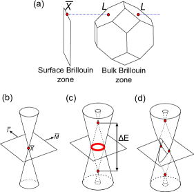
Details of the interface are also important in special cases where two bulk band inversions project to the same point in the surface Brillouin zone (Fig.1a), i.e. they occur at the same in-plane momentum but different perpendicular momenta. Since it is uncommon for semiconductors to possess a direct band gap away from , this condition is rarely satisfied. To date the only experimentally demonstrated examples are the (001) faces of (Pb,Sn)Se and (Pb,Sn)Te.Dziawa2012 ; Tanaka2012 ; Xu2012 A simple analysis would suggest that two degenerate Dirac-like surface states would derive from the two bulk band inversions (Fig.1b). In reality the degeneracy is lifted and the resulting bandstructure features crossings both at and in a ring centered around (Fig.1c). Hybridization eliminates all points of intersection except on the high symmetry line --, where mirror symmetry forbids it. This results in the peculiar band dispersion shown in Fig. 1d.
The lifting of degeneracy depicted in Fig. 1b (henceforth ‘valley splitting’) is the focus of this study. Valley splitting is an interface effect, and cannot be predicted purely from consideration of bulk properties. Symmetry analysis can produce a Hamiltonian that accurately describes the surface bandstructure,Liu2013_prb ; Wang2013 however this approach requires empirical tuning and leaves the physical interpretation of the Hamiltonian parameters unclear. Previous experimental studies have observed that the valley splitting depends on the bulk band-inversion magnitude,Wojek2014 ; Tanaka2013 ; Zeljkovic2015_2 but the mechanism remains to be clarified.
Here we demonstrate an alternative approach to studying the valley splitting, in which we grow heterostructures consisting of thin layers of the normal semiconductor PbSe on the TCI Pb0.7Sn0.3Se. With angle resolved photoemission spectroscopy (ARPES) we are able to observe the evolution of the topological interface state as the normal/TCI interface is buried. To date there are very few spectroscopic studies of buried topological interface states.Berntsen2013 ; Yoshimi2014 ; Eich2016 We show that the magnitude of the valley splitting is extremely sensitive to atomic scale details of the interface, and moreover is non-monotonic with PbSe thickness (summarized in Fig.2). This evolution can be qualitatively explained with a simple effective mass model, accounting for both our results and those of previous studies. Tight binding calculations elucidate that the valley splitting decays with layer thickness, but in addition is strongly suppressed by PbSe steps at intermediate (non-integer) layer coverage.
Results and Discussion
Physical Depth Profile
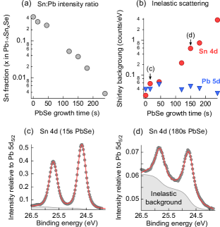
Without leaving ultrahigh vacuum, synchrotron photoemission measurements were performed on the heterostructure samples. Monitoring the intensity ratio of the Sn 4d and Pb 5d core levels (Fig. 3a) offers an in-situ estimate of the growth rate, since lead atoms remain at the surface while tin atoms are buried. As described in the Supplementary Material, this method returns a growth rate of 0.08 Ås-1. This can be corroborated by ex-situ measurements: secondary ion mass spectrometry (SIMS) on the same sample suggests a rate of 0.11 Ås-1, while cross sectional electron microscopy of a thick calibration film indicates a growth rate of (0.10 0.01) Ås-1 (see Supplementary Material). Since electron microscopy is the best calibrated approach, in the remainder of the manuscript we will assume this growth rate when mapping from growth time to film thickness in monolayers (1 ML = 0.306 nm). None of the techniques indicated thickness variation across the sample laterally.
Two important assumptions in these experiments are that the PbSe / Pb0.7Sn0.3Se interface is sharp and that the band ordering of the PbSe layer is normal. Here the two major concerns are segregation of tin atoms and strain of the PbSe layer, since both could result in a band inverted PbSe overlayer. Owing to the low growth temperatures, segregation seems unlikely and indeed the exponentially decreasing core level intensity ratio in Fig 3a suggests that tin atoms remain at the interface. An independent confirmation of this can be obtained from examining the strength of the Shirley background of the core level spectra (Fig. 3b-d). As a function of PbSe thickness, the Pb 5d background is unchanged while the Sn 4d background increases exponentially. This is consistent with the Sn atoms remaining buried at the interface, resulting in increased scattering of the photoelectrons as they travel to the surface. From our measurements it is not possible to evaluate strain in the PbSe layer. The lattice constant of Pb0.7Sn0.3Se (a=6.08 Å) is slightly smaller than that of PbSe (a=6.12 Å), but the thermal expansion coefficients are essentially identical. Hence if no relaxation occurs during growth, biaxial compressive strain of at most 0.7% could be expected. Previous calculations Barone2013 ; Hsieh2012 predict that PbSe requires compressive strain of approximately 2% in order to close the bandgap. We might therefore expect the PbSe bandgap to be reduced, but not closed and certainly not inverted. Due to this low level of strain and film thicknesses below 10nm, we also do not expect the periodic dislocation network seen previously in STM experiments on IV-VI heterostructures with larger lattice mismatches (3%).Springholz2001 ; Zeljkovic2015_2
Bandstructure Measurements
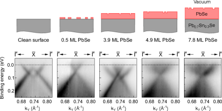
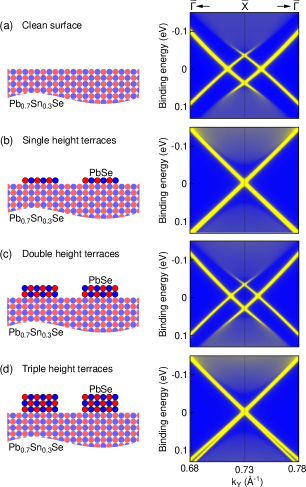
In Fig.4 we show ARPES datasets measured at three different PbSe overlayer thicknesses. The clean surface (Fig. 4a-c) shows the well known double Dirac cone structure, where the energy splitting of two ‘parent’ Dirac cones results in the emergence of two momentum split ‘child’ Dirac points away from . After adding only 0.5 ML of PbSe, the valley splitting of the parent Dirac cones collapses (Fig. 4d-f), taking with it the characteristic Lifshitz transition and associated van-Hove singularities. When an additional 3.4 ML are deposited, the splitting returns (Fig. 4g-i). Note that the constant energy surfaces in Fig. 4h clearly indicate two Dirac points, excluding the possibility that this is a single Dirac cone plus a trivial parabolic conduction band state. Careful inspection reveals that the k∥ dispersion has also changed; the simple model of Liu Liu2013_prb includes such behaviour provided we include higher order terms (discussed in the Supplementary Material). Beyond this thickness the splitting appears to collapse once more, although it becomes difficult to be certain owing to the unavoidable increase in blurring of the spectra from inelastic photoelectron scattering. Several additional growth experiments, summarized in Supplementary Material, show a similar evolution. The striking changes in the surface state dispersion with increasing PbSe thickness constitute the key result of this study, and the discussion that follows is directed at understanding the origin of this behaviour.
The choice of 18 eV as photon energy for the ARPES measurements is significant, partially for high momentum resolution but primarily due to a strong resonant enhancement of the interface state at this energy (also seen on the (111) oriented surface Polley2014 ). The inelastic mean free path for photoelectrons is very short at this energy (2 nm) and we are attempting to measure electronic states localized to a buried interface. However the combination of the exponential decay of the interface state wavefunction towards the surface, the very strong intensity enhancement at h=18 eV and the high photon flux available from a synchrotron source means that the topological interface state can indeed be observed for PbSe layer thicknesses up to at least 8 ML (2.5 nm). A similar approach has enabled the measurement of buried dopant layers in silicon.Miwa2013 ; Miwa2014
Thickness Dependent Energy Splitting
To understand the Dirac cone splitting, useful comparisons may be drawn with the valley splitting of quantum well states hosted by semiconductors such as Si,AndoFowlerStern1982 ; Zwanenberg2013 Ge Carter2013 and AlSb.Ting1988 The effective mass approximation (EMA) is a useful framework here. Under the EMA, eigenstates of a confinement potential at a given momentum are constructed from a basis of all bulk Bloch states with the same in-plane momentum but various perpendicular momenta. The resulting wavefunction can be approximated by a simple envelope function, abstracting away the lattice potential and reducing the problem to that of a simpler quantum mechanical ‘particle in a box’ solution to the bare confinement potential. Several authors have demonstrated that the EMA remains valid with a two-valley bulk basis,Sham1979 ; Ting1988 ; Valavanis2007 ; Saraiva2011 ; Nestoklon2006 in which case two degenerate eigenstates are predicted. However experimentally it has long been known that the degeneracy is usually lifted.AndoFowlerStern1982 The reason is that the two eigenstates will be built from the bulk basis such that they have the same envelope function but differing phases of the underlying Bloch-like oscillation. In free space this has no consequence, but in the presence of a confinement or interface potential the energy eigenvalues slightly differ. In this way the situation is closely analogous to the opening of bandgaps at zone boundaries in the nearly-free-electron model.
Accurately calculating the splitting magnitude is challenging, but certain qualitative aspects are universally agreed on. The magnitude of the splitting is typically small, but increases rapidly with the strength of the confinement potential. It also oscillates as the width of the confinement potential changes on an atomic scale,Ting1988 ; Nestoklon2006 ; Valavanis2007 ; Freisen2007 ; Boykin2008 ; Virgilio2009 reflecting the phase difference between the two eigenstates. Finally, and for similar reasons, the presence of disorder or steps can strongly suppress valley splitting.Goswami2007 ; Zwanenberg2013
The physics described here is independent of the material system or the origin of the confinement potential. It applies to the two-dimensional states formed by electrostatic band bending in field effect transistor inversion layers, semiconductor heterostructures and delta-doping profiles, but also to the mass inversions at the boundaries of topological insulators. However certain properties are unique to band-inverted heterostructures. The wavefunction is peaked at the well walls rather than inside the well, with an envelope function that decays exponentially as:Zhang2012
| (1) |
where is a scalar normalization factor, the bulk bandgap and the bulk band velocity in the direction. Hence to influence the real-space confinement of the wavefunction, it is the magnitude and abruptness of the band inversion that must be tuned. In contrast to regular quantum wells, electric fields are ineffective to tune the envelope function, since this moves the energy positions of valence and conduction bands equally. This can already be seen in the results of previous studies: electrostatic surface doping of (Pb,Sn)Se causes a rigid energy shift but has no effect on the valley splitting,Pletikosic2014 ; Neupane2015 while increasing the band-inversion strength in the bulk by altering composition, temperature or strain increases the valley splitting .Wojek2014 ; Tanaka2013 ; Zeljkovic2015_2 The latter case can be interpreted as pushing the surface state wavefunction towards the strong potential gradient at the TCI-vacuum interface, thus making the effect of the phase difference more pronounced.
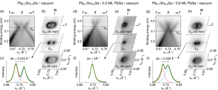
In Fig.5a,b we sketch the situation for Pb0.7Sn0.3Se with a PbSe overlayer. Considering Equation 1 in the limit of a clean surface, the envelope function decays slowly into the Pb0.7Sn0.3Se but abruptly into the vacuum, since vacuum can be considered equivalent to a trivial insulator with infinite bandgap. In contrast, PbSe is a finite gap trivial insulator and establishes a slower, piecewise decay of the envelope on the trivial side (Fig. 5b). As the thickness of the PbSe layer increases, the interface state wavefunction grows wider and the envelope amplitude at both the PbSe/(Pb,Sn)Se and vacuum/PbSe interfaces decreases. In line with the preceding discussion, we should expect this to result in an overall decrease of the valley splitting, accompanied by two-monolayer periodic oscillations. Tight binding calculations of PbSe / Pb0.7Sn0.3Se heterostructures make a similar prediction. Fig.5c plots the surface spectral function for a 16 ML thick PbSe overlayer on Pb0.7Sn0.3Se(001), and demonstrates a small energy splitting. The depth-resolved probability densities at k are in agreement with the preceding discussion, with envelope amplitudes peaked at the PbSe / Pb0.7Sn0.3Se interface and decaying exponentially on either side. The antiphase of the underlying fast oscillations is also apparent. Performing the same calculations as a function of PbSe thickness yields the expected depth-dependent reduction in splitting shown in Fig.5d (grey circles).
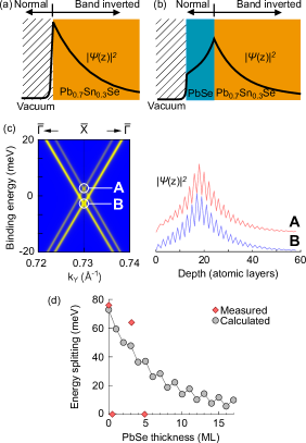
However when these calculations are compared with our experimental results (Fig.5d, red diamonds), it is clear that we observe much larger changes in energy splitting. In particular, without even a full monolayer coverage of PbSe the experimental splitting has apparently completely collapsed. This can be accounted for by considering the additional influence of terraces for non-integer layer coverage.
The Role of Atomic Terraces
Additional tight binding calculations (Fig. 6) illustrate the pronounced effect of surface terraces for the case of partial PbSe coverage. This is achieved by constructing an in-plane structure of 31 atom wide PbSe terraces, aligned to the [110] direction and separated by 19 atoms. This coverage corresponds to 0.62 ML, approximately matching the collapsed Dirac cones in Fig. 4d-f. For odd height terraces there is an almost complete collapse of the splitting, while for even height terraces the splitting is largely unaffected. This is a direct consequence of the antiphase of the two eigenstates, as we discuss in detail in the Supplementary Material. In simple terms if the eigenstates are in antiphase, a shift of the surface position equivalent to a phase shift should exchange bonding and antibonding states. For IV-VI films this occurs every atomic layer. As a result, if the surface is half covered by monoatomic terraces then any fixed phase configuration will integrate to zero splitting.
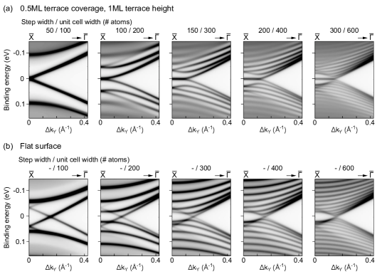
Several authors have studied cleaved surfaces of (Pb,Sn)Se with ARPES.Dziawa2012 ; Wojek2013 ; Pletikosic2014 ; Wojek2014 ; Neupane2015 ; Wojek2015 After accounting for differences in composition and temperature, the dispersion of the Dirac-like states is quite consistent. Scanning tunneling microscopy observations show that these cleaved surfaces consist of atomically flat terraces separated by 50-100 nm.Gyenis2013 ; Sessi2016 Since a typical ARPES light spot is of order m m, it is interesting to consider why atomic steps do not influence the valley splitting of cleaved surfaces but only our PbSe overgrown surfaces. In Figure 7a we summarize tight binding calculations for a Pb0.7Sn0.3Se surface with 0.5 ML terrace coverage, where the lateral size of the terraces are varied (Fig.7a). Note that this is a homostructure, not PbSe terraces on Pb0.7Sn0.3Se. We anticipate similar results in both cases.
Figure 7a reveals a size dependence of the splitting cancellation: for narrow terraces (100 atomic rows, or 21 nm) the valley splitting has collapsed. For wider terraces the splitting is restored, together with a flat band connecting the two Dirac points. The 1D edge state was recently studied by Sessi et al..Sessi2016 For comparison, Fig.7b shows flat surfaces with the same unit cell sizes as in Fig.7a. This comparison demonstrates that the many bands appearing in Fig.7 are due to a bandfolding artifact from the large unit cells. After unfolding the bands only one Dirac cone would be observed in each panel.
In the effective mass model for valley splitting (see Supplementary Material) it is assumed that the wavefunction phase is fixed throughout the entire region of interest, in which case a surface half covered by phase shifting terraces should integrate to zero splitting. If the terrace separation is sufficiently large, the assumption of a fixed phase is no longer valid, i.e. the wavefunction phase is able to adjust between terraces. This is the reason that the 1D edge state and the collapse of the Dirac cone splitting cannot occur simultaneously: the former results from the wavefunction phase difference at the boundaries of odd-height steps, while the latter occurs only when the wavefunction phases are unable to make a phase adjustment between surface steps.
Since cleaved surfaces consist primarily of large terrace widths of 50-100nm (230-465 atoms), the valley splitting is unaffected. For the PbSe overgrown surfaces studied here we expect a much higher terrace density. The small lattice mismatch between the (Pb,Sn)Se substrate and the PbSe layer should result in pseudomorphic growth. Meanwhile the very low growth temperature (close to room temperature) should suppress adatom mobility, causing layer-by-layer growth initiated at many disconnected islands. Previous work on IV-VI MBE on lead-salt substrates has demonstrated clear oscillations in reflection high energy electron diffraction (RHEED) down to the lowest studied substrate temperature of 70℃, a clear indication of a layer-by-layer growth mode.Springholz1994
We thus believe that a dense network of odd-height atomic steps is reponsible for causing the valley splitting collapse, and that these arise due to the low temperature, layer-by-layer partial filling of the large, atomically flat terraces on the cleaved substrate crystal. Such a growth mode would result in both a uniform height distribution and the necessary higher lateral density of steps compared with the cleaved substrate. Future studies combining topographic measurements (e.g. scanning tunnelling microscopy or atomic force microscopy) with ARPES would be valuable to confirm this.
Finally we comment on a potential implication of our observations. Previous studies Liu2014_nmat ; Ezawa2014 have highlighted that 1D edge states in thin (001) oriented films of (Pb,Sn)Se also exhibit degeneracies shifted away from time reversal invariant momenta, and that this could be exploited for electronic devices. Since mirror symmetry can easily be broken by applying an electric field, an electrostatic gate could open a gap at the Fermi level. Our measurements highlight that while the interface degeneracies are robust, the valley interactions responsible for shifting them away from time reversal invariant momenta is fragile and depends sensitively on the atomic-scale condition of the surface. Presumably the same is true of the condition of edges in films. Without these valley interactions, all degeneracies occur as Kramers doublets. Although the remaining degeneracies would not be topologically protected if mirror symmetry were broken (owing to an even number of band inversions), still a substantial rearrangement of the bands would be required to eliminate all Fermi level crossings. It is not clear that the electric field produced by a gate electrode could accomplish this, in which case the proposed device would no longer act as a switch. Atomic-scale control of interfaces is fortunately within the capabilities of modern fabrication techniques, and may prove necessary to realize these device concepts.
Quantized PbSe States
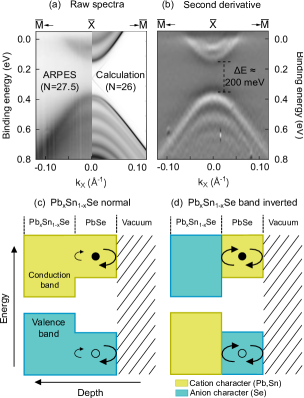
Finally, we examine the outcome when thicker layers of PbSe are grown, shown in Fig.8. With 27.5 ML (8.4 nm), the topological interface states are now buried beyond the probing depth of UV photoemission. As anticipated, the ARPES spectrum now resembles that of trivial PbSe at 130 K, including a 200 meV bandgap.Wojek2014 Careful inspection reveals subband resonances in both the valence and conduction bands, made clearer in a smoothed second derivative image (Fig.8b). Spectral density calculations for a similar PbSe overlayer thickness (Fig.8a, right hand side) reproduce these resonances.
Given that the Pb0.7Sn0.3Se substrate has a smaller bandgap (50 meV Wojek2014 ), a band alignment such as that sketched in Fig.8c would not suggest strong confinement. However carriers in the PbSe layer still experience partial quantum mechanical reflection from the potential step at the PbSe / Pb0.7Sn0.3Se interface. The subband resonances would become more pronounced if the substrate were band inverted, as depicted in Fig.8d and corresponding to the spectra in Fig.8a,b. Now the anion/cation orbital character of the bands is reversed,Hsieh2012 and reflection of carriers at the interface is greatly enhanced (recall that the topological interface state exists because the two materials cannot otherwise electronically couple). This effect should be generic to any topological insulator / normal heterostructure with a sufficiently thin normal layer, and localized in momentum space to the vicinity of the band inversion. An immediate testable implication is that the subband resonances should be weakened by restoring a normal band ordering in the substrate, for example by applying heat or tensile strain. In this way, studying quantization in the overlayer may offer a remote probe of the buried topological interface.
CONCLUSIONS
In summary, by growing thin epitaxial films of the normal semiconductor PbSe on the TCI Pb0.7Sn0.3Se and studying these in-situ with ARPES, we have gained a number of important insights. We have shown that the topological interface state is preserved when encapsulated in a heterostructure, and that ARPES observations of these buried interface states remain possible at depths of at least 8 ML. The valley splitting responsible for the ‘double Dirac cone’ band dispersion is less robust, to the extent that the splitting can be eliminated by non-integer PbSe layer coverage. All of these findings have important implications for future efforts to build electronic devices from topological crystalline insulator materials. Our observations are also relevant as experimental manifestations of valley splitting, a phenomenon that is crucial to the coherent operation of spin-based solid state quantum computer schemes in multi-valley hosts such as Ge and Si.Goswami2007 ; Zwanenberg2013 Finally, we have observed quantized PbSe subbands for a layer thickness of 8.4 nm, and propose that this involves contributions from a type of symmetry confinement. Taken together, our experiments demonstrate that the approach of growing normal overlayers on topological substrates, to date largely unexplored, exposes a wide range of phenomena for further study.
Methods
Heterostructure Fabrication. The substrates for these experiments were single crystal Pb0.7Sn0.3Se, grown ex-situ by the self-selecting vapor-growth method Szczerbakow1994 and cleaved in ultrahigh vacuum to expose a clean (001) surface. All ARPES measurements were performed at a sample temperature of 130 K, bringing the substrates well into the TCI phase. For PbSe growth the samples were allowed to warm to room temperature, after which PbSe was deposited in-situ by an effusion cell loaded with single crystal PbSe, similar to a previously described arrangement.Polley2014 Since PbSe evaporates molecularly,Springholz2007 stoichiometry is expected to be preserved in the grown layers. Substrates were not purposely heated during or after growth, but experienced radiative heating from the effusion cell. Low energy electron diffraction measurements confirmed that the PbSe overlayer retained the (001) orientation of the substrate, with no indication of a reconstruction. Despite the lack of substrate heating, the PbSe layers remained epitaxial and of relatively good quality, as demonstrated by the well defined bandstructures in Figures 4 and 8.
Photoemission Measurements. Photoemission measurements were performed at the I4 beam line in the MAX-IV synchrotron facility,Jensen1997 using eV (ARPES) or eV (core level spectroscopy) p-polarized photons. The sample temperature was maintained at 130 K during measurements. For the ARPES spectra the total energy resolution was approximately 25 meV, with crystal momentum resolution better than Å-1. Additional measurements were performed at the SGM-3 beamline in the ASTRID 2 synchrotron facility; these are described in the Supplementary Material.
Tight Binding Calculations. We employ a nearest neighbour 18-orbital sp3d5 model, with PbSe parameters taken from Lent et al..Lent1986 For Pb0.7Sn0.3Se we have applied the virtual crystal approximation and SnSe parameterization described previously.Safaei2015 We assume that the temperature dependence is dominated by the change of the lattice constant , and rescale our parameterization according to the Harrison rules.Wojek2013 Similarly, biaxial strain is treated by rescaling hopping parameters such that the change in energy gap with strain is in agreement with the experimentally determined deformation potential Simma2009 and elastic constants.Lippmann1971 The spectral densities projected on specific atomic layers have been calculated with the use of a tight-binding Hamiltonian for a semi-infinite system and an appropriate modification of a recursive Green’s function method described by Lopez Sancho.LopezSancho1985
Supporting Information Available
Details of Dirac point valley splitting in the effective mass model, additional photoemission measurements, fitting of the ARPES spectra to a model, details of core level photoemission analysis, ex-situ cross sectional electron microscopy and secondary ion mass spectrometry.
Author Contributions
C.M.P., A.F., M.B, A.G.Č and T.B. performed the PbSe deposition and photoemission measurements. A.S. grew the single crystal (Pb,Sn)Se substrates. P.D. and M.T. performed ex-situ analysis of the samples. R.B. developed the effective mass and tight binding models, and with R.R performed calculations. C.M.P. carried out the data analysis and wrote the manuscript, with input from all authors. All authors contributed to the interpretation.
Acknowledgements
C.M.P. thanks T.B. Boykin and M.A. Eriksson for helpful discussions, and J. Osiecki for creating data analysis software used here. This work was made possible through support from the Knut and Alice Wallenberg Foundation, the Swedish Research Council, the VILLUM FONDEN via the Centre of Excellence for Dirac Materials (Grant No. 11744) and the Polish National Science Centre (NCN) under projects 2013/11/B/ST3/03934, 2014/15/B/ST3/03833 and 2014/15/B/ST3/04489.
References
- (1) Ando, Y. Topological Insulator Materials, J. Phys. Soc. Jpn. 2013, 82, 102001
- (2) Qi,X-L.; Zhang,S.-C. Topological Insulators and Superconductors Rev. Mod. Phys. 2011, 83, 1057
- (3) Bansil, A.; Lin, H.; Das, T. Colloquium: Topological Band Theory Rev. Mod. Phys. 2016, 88, 021004
- (4) Hasan, M. Z.; Kane, C. L. Colloquium: Topological Insulators Rev. Mod. Phys. 2010, 82, 3045
- (5) Zhang, F.; Kane, C. L.; Mele, E. J. Surface States of Topological Insulators Phys. Rev. B 2012, 86, 081303(R)
- (6) Benia, H.M.; Lin, C.; Kern, K.; Ast, C. R. Reactive Chemical Doping of the Bi2Se3 Topological Insulator, Phys. Rev. Lett. 2011, 107, 177602
- (7) Bianchi, M.; Guan, D.; Bao, S.; Mi, J.; Brummerstedt Iversen, B.; King, P. D. C.; Hofmann, P. Coexistence of the Topological State and a Two-Dimensional Electron Gas on the Surface of Bi2Se3, Nat. Commun. 2010, 1, 128
- (8) Valla, T.; Pan, Z.-H.; Gardner, D.; Lee, Y.S.; Chu, S. Photoemission Spectroscopy of Magnetic and Nonmagnetic Impurities on the Surface of the Bi2Se3 Topological Insulator, Phys. Rev. Lett. 2012, 108, 117601
- (9) Pletikosic̀, I.; Gu, G. D.; Valla, T. Inducing a Lifshitz Transition by Extrinsic Doping of Surface Bands in the Topological Crystalline Insulator Pb1-xSnxSe, Phys. Rev. Lett. 2014, 112, 146403
- (10) Neupane, M.; Xu, S-Y.; Sankar, R.; Gibson, Q.; Wang, Y. J.; Belopolski, I.; Alidoust, N.; Bian, G.; Shibayev, P. P.; Sanchez, D. S.; Ohtsubo, Y.; Taleb-Ibrahmimi, A.; Basak, S.; Tsai, W-F.; Lin, H.; Durakiewicz, T.; Cava, R. J.; Bansil, A.; Chou, F. C.; Hasan, M. Z. Topological Phase Diagram and Saddle Point Singularity in a Tunable Topological Crystalline Insulator, Phys. Rev. B 2015, 92, 075131
- (11) Zeljkovic, I.; Okada, Y.; Serbyn, M.; Sankar, R.; Walkup, R.; Zhou, W.; Liu, J.; Chang, G.; Wang, Y. J.; Hasan, M. Z.; Chou, F.; Lin, H.; Bansil, A.; Fu, L.; Madhavan, V. Dirac Mass Generation From Crystal Symmetry Breaking on the Surfaces of Topological Crystalline Insulators, Nat. Mater. 2015, 14, 318-324
- (12) Wojek, B. M.; Berntsen, M. H.; Jonsson, V.; Szczerbakow, A.; Dziawa, P.; Kowalski, B. J.; Story, T.; Tjernberg, O. Direct Observation and Temperature Control of the Surface Dirac Gap in a Topological Crystalline Insulator, Nat. Commun. 2015, 6, 8463
- (13) Zhu, X-G.; Hofmann, P. Topological Surface States on Bi1-xSbx: Dependence on Surface Orientation, Termination and Stability, Phys. Rev. B 2014, 89 125402
- (14) Liu, J.; Duan, W.; Fu, L. Two Types of Surface States in Topological Crystalline Insulators, Phys. Rev. B 2013, 88 241303(R)
- (15) Wang, J.; Liu, J.; Xu, Y.; Wu, J.; Gu, B-L.; Duan, W. Structural Stability and Topological Surface States of the SnTe(111) Surface, Phys. Rev. B 2014, 89 125308
- (16) Safaei, S.; Kacman, P.; Buczko, R. Topological Crystalline Insulator (Pb,Sn)Te: Surface States and Their Spin Polarization, Phys. Rev. B 2013, 88 045305
- (17) Dziawa, P.; Kowalski, B. J.; Dybko, K.; Buczko, R.; Szczerbakow, A.; Szot, M.; Łusakowska, T.; Balasubramanian, T.; Wojek, B. M.; Berntsen, M. H.; Tjernberg, O.; Story, T. Topological Crystalline Insulator States in Pb1-xSnxSe, Nat. Mater. 2012, 11, 1023-1027
- (18) Tanaka, Y.; Ren, Z.; Sato, T.; Nakayama, K.; Souma, S.; Takahashi, T.; Segawa, K.; Ando, Y. Experimental Realization of a Topological Crystalline Insulator in SnTe, Nat. Phys. 2012, 8, 800-803
- (19) Xu, S-Y.; Liu, C.; Alidoust, N.; Neupane, M.; Qian, D.; Belopolski, I.; Denlinger, J. D.; Wang, Y. J.; Lin, H.; Wray, L. A.; Landolt, G.; Slomski, B.; Dil, J. H.; Marcinkova, A.; Morosan, E.; Gibson, Q.; Sankar, R.; Chou, F. C.; Cava, R. J.; Bansil, A.; Hasan, M. Z. Observation of a Topological Crystalline Insulator Phase and Topological Phase Transition in Pb1-xSnxTe, Nat. Commun. 2012, 3, 1192
- (20) Wang, Y. J.; Tsai, W-F.; Lin, H.; Xu, S-Y.; Neupane, M.; Hasan, M. Z.; Bansil, A. Nontrivial Spin Texture of the Dirac Cones on the Surface of Topological Crystalline Insulator SnTe, Phys. Rev. B 2013, 87, 235217
- (21) Wojek, B. M.; Dziawa, P.; Kowalski, B. J.; Szczerbakow, A.; Black-Schaffer, A. M.; Berntsen, M. H.; Balasubramanian, T.; Story, T.; Tjernberg, O. Band Inversion and the Topological Phase Transition in (Pb,Sn)Se, Phys. Rev. B 2014, 90, 161202(R)
- (22) Tanaka, Y.; Sato, T.; Nakayama, K.; Souma, S.; Takahashi, T.; Ren, Z.; Novak, M.; Segawa, K.; Ando, Y. Tunability of the -space Location of the Dirac Cones in the Topological Crystalline Insulator Pb1-xSnxTe, Phys. Rev. B 2013, 87, 155105
- (23) Zeljkovic, I.; Walkup, D.; Assaf, B. A.; Scipioni, K. L.; Sankar, R.; Chou, F.; Madhavan, V. Strain Engineering Dirac Surface States in Heteroepitaxial Topological Crystalline Insulator Thin Films, Nat. Nanotechnol. 2015, 10, 849-853
- (24) Berntsen, M.H.; Götberg, O.; Wojek, B.M.; Tjernberg, O. Direct Observation of Dirac States at the Interface Between Topological and Normal Insulators, Phys. Rev. B 2013, 88, 195132
- (25) Yoshimi, R.; Tsukazaki, A.; Kikutake, K.; Checkelsky, J. G.; Takahashi, K. S.; Kawasaki, M.; Tokura, Y. Dirac Electron States Formed at the Heterointerface Between a Topological Insulator and a Conventional Semiconductor, Nat. Mater. 2014, 13, 253-257
- (26) Eich, A.; Rollfing, N.; Arnold, F.; Sanders, C.; Ewen, P. R.; Bianchi, M.; Dendzik, M.; Michiardi, M.; Mi, J-L.; Bremholm, M.; Wegner, D.; Hofmann, P.; Khajetoorians, A. A. Absence of Superconductivity in Ultrathin Layers of FeSe Synthesized on a Topological Insulator, Phys. Rev. B 2016, 94, 125437
- (27) Barone, P.; Di Sante, D.; Picozzi, S. Strain Engineering of Topological Properties in Lead-Salt Semiconductors, Phys. Status Solidi RRL 2013, 7, 1102-1106
- (28) Hsieh, T. H.; Lin, H.; Liu, J.; Duan, W.; Bansil, A.; Fu, L. Topological Crystalline Insulators in the SnTe Material Class, Nat. Commun. 2012, 3, 982
- (29) Springholz, G.; Wiesauer, K. Nanoscale Dislocation Patterning in PbTe / PbSe(001) Lattice-Mismatched Heteroepitaxy, Phys. Rev. Lett. 2001, 88, 015507
- (30) Miwa, J. A.; Hofmann, P.; Simmons, M. Y.; Wells, J. W. Direct Measurement of the Band Structure of a Buried Two-Dimensional Electron Gas, Phys. Rev. Lett. 2013, 110, 136801
- (31) Ando, T.; Fowler, A. B.; Stern, F. Electronic Properties of Two-Dimensional Systems, Rev. Mod. Phys. 1982, 54 437
- (32) Zwanenburg, F.; Dzurak, A. S.; Morello, A.; Simmons, M. Y.; Hollenberg, L. C. L.; Klimeck, G.; Rogge, S.; Coppersmith, S. N.; Eriksson, M. A. Silicon Quantum Electronics, Rev. Mod. Phys. 2013, 85 961
- (33) Carter, D. J.; Warschkow, O.; Gale, J. D.; Scappucci, G.; Klesse, W. M.; Capellini, G.; Rohl, A. L.; Simmons, M. Y.; McKenzie, D. R.; Marks, N. A. Electronic Structure of Phosphorus and Arsenic -Doped Germanium, Phys. Rev. B 2013, 88, 115203
- (34) Ting, D. Z-Y.; Chang, Y-C. L-Valley-Derived States in (001) GaSb/AlSb Quantum Wells and Superlattices, Phys. Rev. B 1988, 38, 3414
- (35) Sham, L. J.; Nakayama, M. Effective-Mass Approximation in the Presence of an Interface, Phys. Rev. B 1979, 20, 734
- (36) Valavanis, A.; Ikonić, Z.; Kelsall, R. W. Intervalley Splitting and Intersubband Transitions in n-Type Si/SiGe Quantum Wells: Pseudopotential vs. Effective Mass Calculation, Phys. Rev. B 2007, 75, 205332
- (37) Saraiva, A. L.; Calderón, M. J.; Hu, X.; Das Sarma, S.; Koiler, B. Physical Mechanisms of Interface-Mediated Intervalley Coupling in Si, Phys. Rev. B 2009, 80, 081305(R)
- (38) Nestoklon, M. O.; Golub, L. E.; Ivchenko, E. L. Spin and Valley-Orbit Splittings in SiGe/Si Heterostructures, Phys. Rev. B 2006, 73, 235334
- (39) Boykin, T. B.; Kharche, N.; Klimeck, G. Valley Splitting in Finite Barrier Quantum Wells, Phys. Rev. B 2008, 77, 245320
- (40) Virgilio, M.; Grosso, G. Valley Splitting and Optical Intersubband Transitions at Parallel and Normal Incidence in [001]-Ge/SiGe Quantum Wells,Phys. Rev. B 2009, 79, 165310
- (41) Goswami, S.; Slinker, K. A.; Friesen, M.; McGuire, L. M.; Truitt, J. L.; Tahan, C.; Klein, L. J.; Chu, J. O.; Moonery, P. M.; van der Weide, D. W.; Joynt, R.; Coppersmith, S. N.; Eriksson, M. A. Controllable Valley Splitting in Silicon Quantum Devices, Nat. Phys. 2007, 3, 41-45
- (42) Miwa, J. A.; Warschkow, O.; Carter, D. J.; Marks, N. A.; Mazzola, F.; Simmons, M. Y.; Wells, J. W. Valley Splitting in a Silicon Quantum Device Platform, Nano Lett. 2014, 14, 1515-1519
- (43) Freisen, M.; Chutia, S.; Tahan, C.; Coppersmith, S. N. Valley Splitting Theory of SiGe/Si/SiGe Quantum Wells, Phys. Rev. B 2007, 75, 115318
- (44) Springholz, G.; Bauer, G. Low Temperature Growth of PbTe and of PbTe/Pb1-xEuxTe Multi-Quantum Wells by Molecular Beam Epitaxy, J. Cryst. Growth 1994, 144, 157-172
- (45) Sessi, P.; Di Sante, D.; Szczerbakow, A.; Glott, F.; Wilfert, S.; Schmidt, H.; Bathon, T.; Dziawa, P.; Greiter, M.; Neupert, T.; Sangiovanni, G.; Story, T.; Thomale, R.; Bode, M. Robust Spin-Polarized Midgap States at Step Edges of Topological Crystalline Insulators, Science 2016, 354, 1269-1273
- (46) Liu, J.; Hsieh, T. H.; Wei, P.; Moodera, J.; Fu, L. Spin-Filtered Edge States With an Electrically Tunable Gap in a Two-Dimensional Topological Insulator, Nat. Mater. 2014, 13 178-183
- (47) Ezawa, M. Electrically Tunable Conductance and Edge Modes in Topological Crystalline Insulator Thin Films: Minimal Tight-Binding Model Analysis New J. Phys. 2014, 16 065015
- (48) Gyenis, A.; Drozdov, I. K.; Nadj-Perge, S.; Jeong, O. B.; Seo, J.; Pletikosic̀, I.; Valla, T.; Gu, G. D.; Yazdani, A. Quasiparticle Interference on the Surface of the Topological Crystalline Insulator Pb1-xSnxSe, Phys. Rev. B 2013, 88, 125414
- (49) Szczerbakow, A.; Berger, H. Investigation of the Composition of Vapour-Grown Pb1-xSnxSe Crystals (x 0.4) by Means of Lattice Parameter Measurements, J. Cryst. Growth 1994, 139, 172-178
- (50) Polley, C. M.; Dziawa, P.; Reszka, A.; Szczerbakow, A.; Minikayev, R.; Domagala, J. Z.; Safaei, S.; Kacman, P.; Buczko, R.; Adell, J.; Berntsen, M. H.; Wojek, B. M.; Tjernberg, O.; Kowalski, B. J.; Story, T.; Balasubramanian, T. Observation of Topological Crystalline Insulator Surface States on (111)-Oriented Pb1-xSnxSe Films, Phys. Rev. B 2014, 89, 075317
- (51) Springholz, G.; Bauer, G; Molecular Beam Epitaxy of IV-VI Semiconductor Hetero- and Nano-Structures Phys. Status Solidi B 2007, 244, 2752-2767
- (52) Jensen, B. N.; Butorin, S. M.; Kaurila, T.; Nyholm, R.; Johansson, L. I. Design and Performance of a Spherical Grating Monochromator Used at MAX I, Nucl. Instrum. Methods Phys. Res., Sect. A 1997, 394 243-250
- (53) Lent, C. S.; Bowen, M. A.; Dow, J. D.; Allgaier, R. S.; Sankey, O. F.; Ho, E. S. Relativistic Empirical Tight-Binding Theory of the Energy Bands of GeTe, SnTe, PbTe, PbSe, PbS, and their Alloys, Superlattices Microstruct. 1986, 2, 491-499
- (54) Safaei, S.; Galicka, M.; Kacman, P.; Buczko, R. Quantum Spin Hall Effect in IV-VI Topological Crystalline Insulators, New J. Phys. 2015, 17, 063041
- (55) Wojek, B. M.; Buczko, R.; Safaei, S.; Dziawa, P.; Kowalski, B. J.; Berntsen, M. H.; Balasubramanian, T.; Leandersson, M.; Szczerbakow, A.; Kacman, P.; Story, T.; Tjernberg, O. Spin-Polarized (001) Surface States of the Topological Crystalline Insulator Pb0.73Sn0.27Se, Phys. Rev. B 2013, 87, 115106
- (56) Simma, M.; Fromherz, T.; Bauer, G.; Springholz, G. Type I/Type II Band Alignment Transition in Strained PbSe/PbEuSeTe Multiquantum Wells, Appl. Phys. Lett. 2009, 95, 212103
- (57) Lippmann, G.; Kastner, P.; Wanninger, W. Elastic Constants of PbSe, Phys. Status Solidi A 1971, 6, K159-161
- (58) Lopez Sancho, M. P.; Lopez Sancho, J. M.; Rubio, J. Highly Convergent Schemes for the Calculation of Bulk and Surface Green Functions, J. Phys. F: Met. Phys. 1985, 15, 851