Size Constraints on Majorana Beamsplitter Interferometer:
Majorana Coupling and Surface-Bulk Scattering
Abstract
Topological insulator surfaces in proximity to superconductors have been proposed as a way to produce Majorana fermions in condensed matter physics. One of the simplest proposed experiments with such a system is Majorana interferometry. Here, we consider two possibly conflicting constraints on the size of such an interferometer. Coupling of a Majorana mode from the edge (the arms) of the interferometer to vortices in the center of the device sets a lower bound on the size of the device. On the other hand, scattering to the usually imperfectly insulating bulk sets an upper bound. From estimates of experimental parameters, we find that typical samples may have no size window in which the Majorana interferometer can operate, implying that a new generation of more highly insulating samples must be explored.
pacs:
71.10.Pm, 74.45.+c, 73.23.-bI Introduction
There has been an ongoing search for Majorana fermions in condensed matter systems which has been intensified over several years. Alicea (2012) Vortices in a spinless -wave superconductor have long been known to bind zero energy Majorana modes.Read and Green (2000); Kopnin and Salomaa (1991); Volovik (1999); Gurarie and Radzihovsky (2007) With -wave superconductors being very rare in nature, no experiment has convincingly observed such Majoranas yet.Kallin and Berlinsky (2016) More recently it was predicted that Majorana bound states also exist in vortices in a proximity-induced superconductor on the surface of a topological insulator (TI).Fu and Kane (2008) A number of recent experiments on TIs in proximity to superconductorsQu et al. (2012); Flinck et al. (2016); Sasaki et al. (2011); Xu et al. (2014); Koren et al. (2011); Zareapour et al. (2012) and other similar experimental systemsMourik et al. (2012); Nadj-Perge et al. (2014) have increased the interest in this possibility.

The surfaces of TIs support gapless excitations with the dispersion of a Dirac coneHasan and Kane (2010) (in principle, TIs can have any odd number of Dirac cones in the Brillouin zone but we consider the simplest case of a single cone for simplicity). The spectrum can be gapped either by applying a magnetic field to give the Dirac fermion either a positive or negative mass, or by placing a superconductor in proximity to the surface. At interfaces between different gapped regions, gapless one-dimensional fermionic channels can develop. For example, an interface between two magnetically gapped regions with opposite mass signs will contain a gapless and chiral one-dimensional Dirac fermion mode. An interface between a magnetically gapped region and a superconducting region will contain a gapless chiral Majorana mode.Fu and Kane (2008); Akhmerov et al. (2009); Fu and Kane (2009) It is the physics of these modes that we are exploring in the current paper.
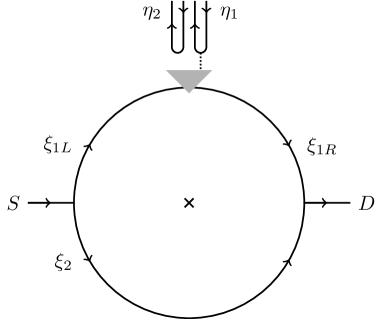
A very elegant experiment, building an interferometer out of these gapless chiral modes, was proposed by Fu and KaneFu and Kane (2009) and simultaneously by Akhmerov et al.Akhmerov et al. (2009) The device is depicted schematically in Fig. 1. Incoming particles or holes, biased at a low voltage, flow into a Dirac channel between two oppositely polarized magnetic regions. The Dirac fermion is split into two Majorana fermions upon hitting the superconductor, one flowing in each direction around the superconducting region (drawn as a disk in Fig. 1). At the other end of the superconducting region the two Majorana modes are re-combined into a Dirac mode. The differential conductance of this device was predicted to take the values or depending on whether the number of vortices in the superconductor is even or odd, respectively. With the exception of quantum Hall systems, this was the first proposed realistic Majorana interferometry experiment, and it remains a good candidate for the first experiment to successfully establish the existence of chiral Majorana modes (although, we note that promising evidence of chiral Majorana modes was reported very recentlyHe et al. (2017)).
The most experimentally explored TI materials are the Bismuth based compounds,Ando (2013); Ortmann et al. (2015); Hasan and Kane (2010, 2010) including (among many others) Bi2Se3, Bi2Te3, and Bi2Te2Se. Within this class of materials, several experiments have successfully formed some sort of superconducting interfaces.Qu et al. (2012); Flinck et al. (2016); Sasaki et al. (2011); Xu et al. (2014); Koren et al. (2011); Zareapour et al. (2012) In this paper we mainly have this type of material in mind. However, we note that the material SmB6,Wolgast et al. (2013); Zhang et al. (2013) which is possibly a topological Kondo-insulator, will be discussed in the conclusion.
In this paper we study two effects that restrict the size of the interferometer device, as summarised in Fig. 2. On the one hand, we consider coupling of the Majorana edge mode to the Majorana modes trapped in the core of the vortex in the center of the interferometer. When this coupling is sufficiently strong, i.e. when the interferometer is sufficiently small, the conductance signal will be distorted, rendering the interpretation of the experiment difficult. The coupling is generally strong on the scale of the coherence length where is the Fermi velocity and is the proximity gap. This length scale can be on the order of a micron (we discuss materials parameters in section III.1, IV.2, and IV.3).
Next, we consider surface-bulk scattering due to the unintentionally doped and poorly insulating bulk of TIs.Checkelsky et al. (2009); Ando (2013); Skinner et al. (2013) We find that when current leaks from the Majorana edge channel to the ground, the signal obtained at the end of the interferometer drops exponentially with a length scale set by the surface-to-bulk scattering length from disorder. For typical samples this length scale can be shorter than a micron. Thus we have two potentially conflicting constraints on the size of the proposed interferometer. We will discuss the possible directions forward in the conclusion.
The outline of this paper is as follows. In section II we review the formalism of Majorana interferometry and the characteristic conductance signal of the experiment. In section III we consider the impact of coupling between the chiral Majorana and a bound Majorana mode in a vortex core. We study how this limits the source-drain voltage and sets a lower bound on the size of the system. In section IV we consider the leakage of current from the device to the TI substrate and we establish an upper limit on the system size due to this leakage. We conclude with numerical estimates and an outlook for Majorana interferometry on the surface of TIs. Appendix A contains a derivation of the average currents. In Appendix B we provide generalizations of the single-point Majorana coupling displayed in Fig. 2 (a). Vortex-bound Majorana fermions in a TI/SC hybrid structure and the energy splitting between zero modes is discussed in Appendix C. In Appendix D we present details of our estimate of the surface-bulk scattering rate based on Fermi’s Golden rule. Finally, in Appendix E signal loss due to scattering with acoustic phonons is briefly discussed.

II Background on Interferometry with Majorana Fermions
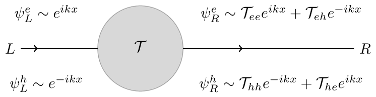
In this section, we first review the formalism needed to calculate the conductance and interferometry current.Fu and Kane (2009); Akhmerov et al. (2009); Law et al. (2009); Li et al. (2012) In Fig. 2 (a) we show a top view of the interferometer that was described in the introduction. For the moment we ignore the Majorana coupled to the top arm (marked as an “X”) at position 0. Charge transport from the source to the drain is computed by using a transfer matrix which describes transport of particles and holes from the source on the left (), via the perimeter of the superconductor, to the drain on the right (), where T here means transpose. The matrix can be decomposed into three pieces corresponding to the three key steps between the source and the drain
| (1) |
The unitary matrix relates the Majorana states running along the upper and lower edge of the superconducting disk to the electron and hole states that enter via the leads, . The matrix contains plane wave phases that the low energy chiral Majorana modes accumulate as they move along the edge of the superconducting disk. Finally, the matrix reassembles the two Majoranas into outgoing electron and hole states that enter the drain.
The matrices and are functions of energy. Due to the particle-hole symmetry, we must have , where is a Pauli matrix in particle-hole space. At these constraints fix up to an overall phase that observables do not depend on,Akhmerov et al. (2009)
| (2) |
We will apply with for convenience. As discussed in Ref. Fu and Kane, 2009 this form is exact when the system has a left-right symmetry. Even in cases where the system breaks this symmetry, corrections are and can thus be ignored at low temperature and low voltage (see Appendix C.1). We study the symmetric situation where the magnetization is throughout the main text. The magnetization enters the model Hamiltonian given in Eq. (48).
The transfer matrix is used to calculate the average current in the drain as the difference between the electron and hole current, with the source biased at voltage (see Appendix A for a derivation),
| (3) |
Here, with , and is the Fermi-Dirac distribution with and measured relative to the Dirac point. The incoming current is
| (4) |
By current conservation, a net current of is absorbed by the grounded superconductor. As follows from Eq. (3), (4), and unitarity of the differential conductance measured in the grounded superconductor at zero temperature is:
| (5) |
In order to calculate we need only establish the properties of the propagation matrix . If the arms of the interferometer are of length and we have
| (6) |
Above the wavevector is of the form due to the linear dispersion of the Majorana modesFu and Kane (2009) where is the Majorana velocity. We have included an additional phase shift which may come from a number of sources. In Refs. Fu and Kane, 2009; Akhmerov et al., 2009 the possibility of vortices being added in the center of the superconducting region was considered. In this case the additional phase is . Inserting into Eq. (1) and (5) at zero temperature yields the conductance
| (7) |
Here, is the difference between the lengths of the two arms. At , for odd, and is zero for even. This would be a rather clear experimental signature. For the same phase matrix , the drain current in Eq. (3) evaluates to
| (8) |
which holds in the low temperature and low voltage limit (compared to the bulk gap). We emphasise that these results are derived with zero coupling to the central Majorana and to any other degrees of freedom (e.g. phonons or conducting bulk states), hence the subscript .
III Effect of Majorana Coupling
We now consider the effect of coupling the Majoranas trapped in the cores of vortices in the superconductor to the chiral edge states. Each vortex traps a single Majorana mode. If a vortex is close to the edge (roughly within the coherence length) there will be tunnelling coupling as shown in in Fig. 2 (a) where the Majorana zero mode is marked as an “X” and the (tunnelling) coupling matrix element is of magnitude . The magnitude of the coupling drops exponentially with the distance between the vortex and the edge, see Appendix C.2 and C.3.
We very generally describe the chiral Majorana on the upper interferometer arm, , by a Lagrangian density where is the spatial coordinate along the upper edge. A similar description holds for the state on the lower edge, . The vortex bound Majorana, , is described by . We add the coupling term between the central bound state and the chiral mode
| (9) |
The equations of motion, following from the full Lagrangian , are given by Fendley et al. (2009); Bishara and Nayak (2009)
| (10) | ||||
| (11) |
Here, the notation and was introduced. A Fourier transformation yields a phase shift across the coupling point,
| (12) |
with the frequency, , and . This energy-dependent phase shift is inserted into Eq. (6) and we obtain the zero-temperature result
| (13) |
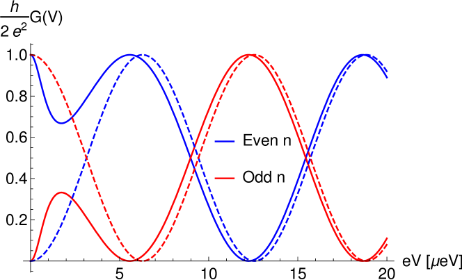
Observe that the even-odd effect undergoes a crossover when the coupling strength is of the order . At zero voltage, or at infinite coupling strength, the even-odd effect is reversed from the value at high voltage or low coupling strength. This crossover is equivalent to shifting by one in , causing to acquire a phase shift of at low energy, and it is assigned the interpretation that a vortex Majorana effectively is absorbed by the edge.Fendley et al. (2009) Similar results are known from Quantum Hall interferometers at filling fraction . Rosenow et al. (2008, 2009); Bishara and Nayak (2009) The original conductance is recovered at high voltage (see Fig. 3).
The above result applies when there is no position dependence in the coupling to the edge. If we instead consider a continuous bulk-edge coupling
| (14) |
then the total phase shift is again given by Eq. (12) with
| (15) |
in the numerator and a similar replacement in the denominator, see Appendix B.1. We note that if , where is defined such that , then the effective above becomes with up to corrections of order .
The scheme above can also be generalized to include more complicated couplings to multiple (vortex) Majorana modes. So long as these modes are coupled to only a single edge, and not to each other, each coupling causes a phase shift of in the phase of propagation along the edge, see Appendix B.2. In the case that multiple vortex Majoranas are coupled to each other, an even number of Majoranas will gap out, whereas an odd number will leave a single effective Majorana zero mode.
In the above calculation we assumed Majorana coupling to one edge only. Since coupling varies exponentially with distance to the edge it is not unreasonable that this will effectively be the case. However, it is also realistic that a vortex will be roughly equal distance from, and hence equally coupled to, both edges. This case is discussed in detail in Appendix B.3. While the general result becomes complicated, at least in the case of equal couplings to both edges and both edges of equal length, the physics of the even-odd crossover found in this section remains unchanged. Finally, coupling between a single vortex Majorana and the edge at finite temperature is discussed in Appendix B.4.
III.1 Lower Bound on Size and Voltage Constraints
The above derived crossover makes the observation of the even-odd conductance effect impossible at low voltage. The proposed experiment is to add a single vortex and observe a change in conductance (say, from zero to ). However, if the Majorana is then effectively absorbed into the edge, the conductance remains zero even once the vortex is added, destroying the predicted effect. This will occur for interferometers of size comparable to the coherence length, i.e. the length scale of an order-parameter deformation. Assuming that meV is an achievable proximity-induced gap in e.g. Bi2Se3,Koren et al. (2011); Sasaki et al. (2011) the naive lower size bound for the disk is m.Zhang et al. (2009a) The tunnelling coupling is expected to decay like when (see Eq. (52)) where is the chemical relative to the Dirac point.Akzyanov et al. (2015) For disks of size the energy splitting is comparable to the energy gap and the notion of stable edge/vortex states breaks down.
We note, however, that the Majorana coupling term vanishes identically at in the topological insulator superconductor hybrid structure.Cheng et al. (2010); Chiu et al. (2015) This is related to appearance of an additional symmetry at the Dirac point, bringing the Hamiltonian (Eq. (48) in the absence of a magnetic field) from symmetry class D to the BDI in the Altland-Zirnbauer classification. If there is disorder inducing local fluctuations in the chemical potential (see section IV.3),Beidenkopf et al. say on some scale , a random coupling term of the type in Eq. (14) will be present and cause energy splitting. Still, the scenario of having the average , which would make the parasitic phase shift vanish, is possible but becomes extremely geometry sensitive (e.g. sensitive to the vortex position) if . Moreover, we should expect to be on the scale of , which in general will not be small. Here, is the length scale associated with the energy fluctuations. Assuming that we cannot control disorder, the only way to assure suppression of unwanted phase shifts and energy splitting is to increase . Thus, we will use as a strict lower size bound on the device.
As far as chiral transport on the interferometer arms is concerned, it seems at this stage that one can operate at high voltage, to avoid the coupling. Naturally, the voltage is constrained from above by the global bulk gap, , to avoid excitation of non-topological states. Thus, if the remaining voltage range, , might be too limited to have a clear experimental signature. Increasing the disk radius to suppress the coupling (and therefore lower ) induces the problem of signal leakage to conducting bulk states, which we estimate below.
Finally, we note that the upper voltage bound in practice can be lower. This is due to the Caroli-de Gennes-Matricon excited states of the vortex, characterised by a minigap, ,Caroli et al. (1964); Möller et al. (2011); Mizushima and Machida (2010) which can be less than one mK. The excited vortex bound states can be activated thermally or by tunnelling from the edge states, in analogy to the zero mode tunnelling in the beginning of this section. By pinning the vortex to a hole in the superconductor, the minigap can be increased to a substantial fraction of . Rakhmanov et al. (2011); Akzyanov et al. (2014) Although the details of such a tunnelling process is outside the scope of this paper, additional resonances and conductance phase shifts are expected as hits the bound state energies.
IV Surface-Bulk Scattering
Topological qubits are intrinsically protected from decoherence. Nayak et al. (2008) In protocols based on braiding with topological qubits, leakage of current is harmful since it generically causes entanglement with the environment that potentially corrupt the qubits.Fu and Kane (2008) Although the experiment we study here does not probe a topological qubit, both types of experiment are sensitive to bulk leakage. Since most TIs are poorly insulating,Ortmann et al. (2015) bulk leakage is a relevant problem to consider.
In this section we model leakage of Majorana modes from the the surface of the TI to its poorly insulating bulk. This is done by coupling the interferometer arm first to a single metallic lead. Then, we take multiple weakly coupled metallic leads to represent a continuously leaking environment. We combine the result of this scattering process with an estimate of the surface-to-bulk scattering rate from disorder in doped TIs. Our results suggest an upper size bound that potentially coincides with the lower bound discussed in section III for many unintentionally doped TIs.
IV.1 Scattering on Conducting Leads
Let the upper interferometer arm be coupled to a metallic lead as depicted in Fig. 2 (b). Referring to the formalism of Ref. Li et al., 2012, the lead fermions are transformed to a Majorana basis, with the superscript indicating incoming () or outgoing () states. The matrix here may differ from the one in Eq. (2) at low energy only by having a different phase , which is irrelevant for observables. The scattering process in the Majorana basis is denoted by ,
| (16) |
By rotating the lead particles and holes into the appropriate Majorana basis, the chiral Majorana mode can be shown to decouple from one of the (artificial) lead Majoranas.Li et al. (2012) In the low energy limit, the scattering matrix is a real rotation matrix, . If we denote the local reflection amplitude of () by (), this means that the scattering matrix can be parametrized by at the junction only (the transmission amplitude is ),
| (17) |
Including the state on the lower arm and the plane wave phases acquired across the interferometer, we obtain the matrix acting on ,
| (18) |
Here, was used. The transfer matrix can be computed, and it has the sub block structure
| (19) |
Above, the subscripts indicate the result of transport from/to the source (), the drain (), or the incoming/outgoing lead (). The blocks in this transfer matrix are used to find the average current contribution as measured in contact , with
| (20) |
Here, the first line gives the contribution from combining Majoranas and , the second line from combining and , and the third line from combining and . Combining Majoranas from different sources always give a vanishing contribution to the average current.Li et al. (2012)
The drain current is thus , where is defined in Eq. (8); the visibility is coherently reduced by . The current in the outgoing lead is at when the lead is biased at . Subtracting the incoming current yields a net current of in the conducting lead. When decoupling the lead completely, , no net current goes in the lead.
The matrix can be trivially extended to include scattering on many single-mode leads. Repeating the calculation above with two scattering leads of the same reflection amplitude gives the same reduction of current in both leads, independent of which arms the leads are coupled to. The drain current is reduced by . Generalising these statements by induction,111This can be proven formally; the proof is a straightforward generalization of Eq. (18) and (19) when identifying the structure of the sub blocks in . Blocks characterizing transport between different leads always give a vanishing contribution to the average current, related to the observation right below Eq. (20). If two leads are not causally connected by the chiral arm, the corresponding block in the matrix is zero. Finally, no matter which arms the leads are coupled to, the drain current is reduced by the factor , where is the local reflection amplitude of lead . with identical scatterers of reflection amplitude , the total conductance from the collection of leads (representing the bulk of the TI) is . Furthermore, the scatterers reduce the visibility of the drain current multiplicatively as .
If we let denote the average length a chiral Majorana travels before it scatters into the bulk, we may by definition express the reflection amplitude as , which is equivalent to defining the leakage conductance into the collection of leads by . Taking the continuum limit of infinitely many weak scatterers means that , and the current is exponentially suppressed in the drain,
| (21) |
As for the differential conductance measured in the grounded superconductor, the amplitude of the oscillations are suppressed
| (22) |
and distinguishing even from odd is rendered difficult as surpasses . Thus, acts as an upper bound on the circumference of the length of the interferometer arms.
IV.2 The Surface-Bulk Scattering Rate
The remaining step of our argument is to estimate the scattering length . We start by calculating the surface-bulk (SB) scattering length for a TI surface electron () in the absence of any surface superconductor or magnet. Then, we use a similar calculation to estimate the Majorana scattering length (). We restrict ourselves to elastic (zero temperature) surface-bulk scattering, where the electron-phonon coupling is irrelevant (see subsection IV.4 and Appendix E). Building on the formalism developed in Ref. Saha and Garate, 2014 we consider scattering via screened charge impurities. We note that the consideration in Ref. Saha and Garate, 2014 is restricted to point scatterers where the overall scattering strength is a priori unknown, whereas in our approach the effective potential strength is fixed by the screened Coulomb potential and the dopant concentration.
Specifically, we consider a surface state () with initial wave vector that scatters to a lowered conduction band (a charge puddle) in the bulk () with final wave vector . The incoming surface state has energy . For numerical purposes we work with a TI slab of thickness nm. In Fig. 4 (a) we show the form of at zero parallel momentum for the lowest three eigenstates (derived in Ref. Shan et al., 2010). One of the TI surface states, penetrating tens of Ås into the bulk, is seen in purple. Assuming randomly distributed screened (dopant) charges with average concentration we get the scattering rate from Fermi’s Golden rule (cf. Appendix D):
| (23) | ||||
Here, is the dispersion of bulk band defining the outgoing wave vector by . The differential scattering rate is the screened Coulomb coupling convoluted with the overlap between the bulk and surface states (cf. Eq (59)), see Fig. 4 (c).
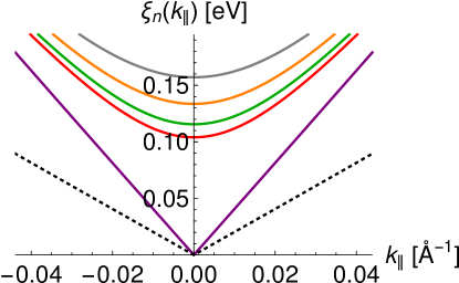
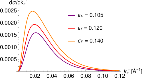
In most topological insulators the Fermi level resides in the bottom of the conduction band or the top of the valence band, and a significant doping of acceptors/donors is needed to reach a bulk insulating state.Hsieh et al. (2009); Skinner et al. (2013) For Bi2Se3 films (typically being -doped) we use the dopant concentration cm-3. Li et al. (2017); Skinner et al. (2013); Borgwardt et al. (2016) Such doping causes fluctuations in the average (doping) concentration, making the conduction band bend and induce electron and hole puddles,Skinner et al. (2013); Beidenkopf et al. i.e. effectively filled pockets from the conduction band at the Fermi level. As a simple model of a typical situation we imagine that chemical doping of the TI bulk lowers the bulk Fermi level to lie in some region eV eV relative to the Dirac point. This would naively be bulk insulating since the Dirac point in Bi2Se3 is separated from the conduction band by a gap of eV.Xia et al. (2009) Puddles coming from stretching the bottom of the conduction band are simply modelled by setting the TI gap to eV, making elastic scattering to the puddles (i.e. the lowered conduction bands) allowed at the Fermi level, see Fig. 4 (b). This captures the generic features in unintentionally doped TIs.
In order to consider scattering from the surface state into the bulk, we need to know how close the surface Fermi energy is to the Dirac point. Note that, as we will see below, the scattering rate increases strongly if we are not very close (compared to ). Let us therefore assume that the surface Fermi energy is tuned near the Dirac point. The electronic scattering rates as a function of the bulk Fermi energy are shown in Fig. 4 (d). We note that the rate stays similar in magnitude for a large TI film thickness range. When the film is made thinner, there are fewer bulk states to scatter into, but this is compensated by an increased surface-bulk overlap. Moreover, the rates in Fig. 4 (d) have the same qualitative features as seen for point source scattering.Saha and Garate (2014)
The (elastic) scattering lifetime of the surface electrons is , and the scattering length is given by . As a typical value of the rates in Fig. 4 (d) we use eV, and we arrive at the unusually long scattering time ns ( mm). This is typically a factor of longer than for bulk scattering lifetimes seen in experiment.Borgwardt et al. (2016) Yet, our results could be consistent with what was attributed to be unusually long surface lifetimes as observed after optically exciting bulk states.Sobota et al. (2012); Neupane et al. (2015) In Ref. Sobota et al., 2012 one deduced that ps after seeing a stable population of the surface state induced by elastic bulk-surface scattering in Bi2Se3 (the samples were kept at K) after subsequent inelastic decays associated with much shorter time scales. It would be desirable to see similar experiments engineered to measure the elastic surface-bulk scattering rate in doped compounds conducted at lower temperatures.
IV.3 Velocity Suppression and Contradicting Requirements
We now use the same expression in Eq. (23) to extract information about the Majorana lifetime and scattering rate. In doing so we ignore the (confined) transverse profile of the Majorana surface state. This is a valid approximation because the reciprocal coherence length is far less than the maximal transverse scattering momentum in the studied energy regime, see Appendix D.1. Moreover, we assume that the induced superconductivity does not gap the TI bulk such that elastic surface-bulk scattering is not precluded. The Majorana scattering rate will typically be larger or equal to the electronic scattering rate due to a suppression of the Majorana velocity relative to the Fermi velocity.
The Majorana velocity is calculated from the low-energy chiral solution of the Hamiltonian in Eq. (48): .Fu and Kane (2009) Here, is the surface chemical potential relative to the Dirac point. From the dependency of in Eq. (23) we deduce that is suppressed approximatively as with (up to some prefactor of order ).222The prefactor of in Eq. (23) has a dependency. There is, however, also a less significant dependency on in , which can be inferred from Fig. 4 (b) (recall that ) to be very close to linear. Correspondingly, . A non-zero size window for the interferometer size is required by imposing , which in turn means that
| (24) |
Inserting the electronic rate from the end of the last subsection and m in this yields . Hence, we must require a very fine tuning of , meV given that one can achieve .
When the TI bulk is increasingly doped with screened Coulomb charges to make the Fermi energy approach the Dirac point, fluctuations in the surface electrical potential energy are enlarged. The spatial dependence of the local density of states broadens the Fermi energy into a Gaussian distribution of finite width. The standard deviation of this energy smearing has been estimated in theorySkinner et al. (2013) and measured in experimentBeidenkopf et al. to be meV within some eV from the average Dirac point ( decays inversely proportional to the average chemical potential further away). For Fermi energies close to the average Dirac point the notion of a uniform local density of states breaks down. Tuning of the surface chemical potential is consequently not globally possible within an energy resolution set by the distribution width.Borgwardt et al. (2016) Importantly, the smearing greatly exceeds the tuning required above, , even if we relax the assumption of a very small by increasing it one order of magnitude.
Finally, the spatial scale of the chemical potential fluctuations is nm. Hence, a precise tuning of the chemical potential might be possible within local regions of this size. Still, this would not help in probing the experiment since . Thus, unless these spatial fluctuations in the local density of states can be brought under control, unintentionally doped TIs are left unsuited for Majorana interferometry.
IV.4 Other Limitations
Majorana interactionsChiu et al. (2015) and coupling between Majorana modes and other degrees of freedom, such as phonons, are other potential sources of decoherence. Local interactions between chiral Majorana fermions are expected to be heavily suppressed at low temperatures and momenta with the leading order term going like . Fu and Kane (2009) The chiral Majoranas on the interferometer arms can also excite phonons if an electron-phonon coupling is present; see Appendix E for a short discussion. For spatial inversion symmetric materials, e.g. Bi2Se3 and Bi2Te3, where this coupling is dictated by a deformation potential, the decay rate of quasiparticles due to scattering on acoustic phonons at exhibits a behaviour. This is a posteriori expected to be small compared to bulk leakage at low voltage. Without spatial inversion symmetry, a piezoelectric interaction can cause the electron-phonon coupling to follow a reciprocal power law in , making scattering an increasing problem for small momenta.
V Conclusions
Two limiting effects in Majorana interferometers are considered. We include a previously neglected coupling between chiral Majoranas and vortex-pinned modes. At low voltage this coupling yields a crossover in the conductance even-odd effect, distorting the interpretation of the experiment. We also find that surface-to-bulk scattering in the TI sets an upper bound on the size of the device. With a proximity gap of meV, the lower bound (the coherence length) is about m for Bi2Se3. Due to the doping needed to reach a bulk insulating state in many TIs, conduction band puddles lead to large fluctuations in the surface Fermi energy. In turn, this is in conflict with the surface chemical potential fine tuning required to have a non-zero size window for the interferometer. This leaves the possibility of probing the experiment in many poorly bulk insulating Bismuth compounds potentially extremely difficult.
The most natural ways to overcome the restrictions considered here are (i) to find superconductors with excellent contact to the TI such that can be made (ideally orders of magnitude) larger, or (ii) to pursue a search for TIs with a highly insulating bulk. Most Bismuth based TIs are poorly insulating and are unintentionally doped,Ando (2013) which results in them being unsuited for Majorana interferometry. However, recently reported mixed Bismuth compounds have shown evidence of an appreciably insulating bulk,Kushwaha et al. (2016) which could potentially open a window of opportunity for this material. We note that the recommendation (i) above is similar to the need for high-quality interfaces in superconductor-semiconductor nanowire devices.Lutchyn et al. (2017)
Another possible material system to consider is the putative topological Kondo insulator SmB6, which gives strong sign of surface conduction.Zhang et al. (2013); Kim et al. (2013) The bulk resistivity of this material can reach several cm at temperatures below a few Kelvins.Zhang et al. (2013) Very recently, evidence of the superconducting proximity effect in Nb/SmB6 bilayers was reported,Lee et al. (2016) hence providing a possible platform for this experiment. However, the physics of highly interacting topological Kondo insulators is still poorly understood, Zhang et al. (2009b); Wolgast et al. (2013) and it is unclear how much of the details of the simple non-interacting TI surface physics will carry through to this more complicated case.
Acknowledgements.
We thank Mats Horsdal, Dmitry Kovrizhin, Ramil Akzyanov for useful discussions and Kush Saha for feedback on the numerics. H. S. R. acknowledges Aker Scholarship. S. H. S. is supported by EPSRC grant numbers EP/I031014/1 and EP/N01930X/1.Appendix A Derivation of the Average Current
The derivation of Eq. (3) and (4) goes along the lines of Ref. Büttiker, 1992. The scattering states of the interferometer are (chiral) plane waves in the one-dimensional channel convoluted with a transverse wavefunction (we let by definition below),
| (25) | ||||
| (26) | ||||
| (27) | ||||
| (28) |
We have assumed that the contacts contain only single mode states and that the incident state in the contact is either an electron or a hole.
One can construct arbitrary states by expanding in the scattering states above. This is incorporated in the (second quantized) field operator
| (29) |
where we introduced and the annihilation operator of type satisfying
| (30) |
The current operator of type in contact is defined by
| (31) |
Here, is the effective mass, . Assuming further that the contacts act as thermal reservoirs kept at equal temperature, we can average the density operator by
| (32) |
where is the Fermi function for particles and holes. Finally, we assume the transverse wavefunctions to be orthonormal,
| (33) |
The source and the drain current are defined by the average particle minus hole current, and . Calculating these explicitly by using Eq. (31), (32), (33), and unitarity of leads exactly to the expressions in Eq. (3) and (4).
Appendix B Charge Transport with Majorana Coupling Disorder
B.1 One Majorana with Smeared Coupling to the Edge
Consider the case where the edge Majorana is coupled continuously to the bound state as in Eq. (14). Using the ansatz with being the Majorana (fermion) field on the far left and for the linearly dispersing modes. The equations of motion can be combined to give the continuum version of Eq. (12):
| (34) |
Here, the plane wave phase contribution that can be neglected in the discrete case where is included. The equation above can be solved as follows. Integrating both sides gives the solution implicitly by
| (35) |
with . Inserting this back into (34) yields
| (36) |
Finally, this expression is used in (35), and we obtain
| (37) | ||||
Comparing this to Eq. (12) proves the statement in Eq. (15).
B.2 Multiple Majoranas Coupled to Each Edge
In the main text, we obtained a phase contribution of in the differential conductance when the edge was coupled to one vortex (Eq. (13)). This can be generalized if the chiral Majoranas have single-point couplings to several vortices. In that case is replaced by , where comes from vortex-edge-coupling with the upper edge and from coupling with the lower edge. Hence, multiple phase crossovers will occur if several vortices are located close to the edge.
B.3 One Majorana Coupled to Both Edges
Another generalization is to study point-couplings to both the lower and the upper arm, in which case the coupling term in the Lagrangian is . The corresponding equations of motion are
| (38) | ||||
| (39) | ||||
| (40) |
Here, we again use the notation , , , and . In frequency space we find a relation between and across the coupling points, , where is the unitary matrix
| (41) |
Above, and . Notice how is off-diagonal in the low-energy limit for the configuration . The chiral Majoranas on the perimeter therefore switch place by tunnelling across the vortex Majorana in this case. The phase matrix is given by
| (42) |
which leads to the differential conductance
| (43) | ||||
This reduces to Eq. (13) when . For the expression above is identical to Eq. (13) with the replacement .
B.4 One Majorana Coupled to One Edge at Finite Temperature
We return to the case with a one-point Majorana coupling (Fig. 2 (a)). The drain current can generally be re-expressed as a residue sum over poles in the upper complex half-plane. Rewriting Eq. (3),
| (44) |
where is the function
| (45) |
The set of simple poles of in the upper half-plane is . For , the sum is obtainable in closed form and stated in Eq. (8).
For weak coupling at finite temperature, , we expand in powers of , with . For convenience we define the reduced current as . To second order in with we find
| (46) | ||||
Above, is the trigamma function. In the infinite coupling limit the sign of the drain current is flipped, , which can be seen from Eq. (45). The reduced current decreases monotonically, a feature of setting , with coupling strength until the vortex Majorana is fully absorbed by the edge.
At the current is found to be (with here):
| (47) | ||||
Here, and are trigonometric integral functions. For symmetric arms the above result simplifies to give the reduced current . From this, the aforementioned result follows trivially.
Appendix C Majorana Fermions in a TI/SC Hybrid Structure
Superconductivity induced on the surface of a strong TI support chiral Majorana fermions on domain walls and Majorana bound states localized in vortices. The Fu and Kane Hamiltonian of a TI/SC hybrid structure with a single Dirac-like dispersion is given by Fu and Kane (2008, 2009)
| (48) |
where and are Pauli matrices acting in particle-hole and spin space, respectively. Moreover, and is the Zeeman energy associated with a magnetic field applied in the direction. The standard procedure is to introduce and that define the quasiparticles, conveniently arranged in satisfying the BdG equations .
C.1 Corrections to the Matrix
One may solve Eq. (48) on a magnetic domain wall in the absence of a superconductor. There are then two chiral solutions: one in the particle sector, , and one in the hole sector, , both localized at the interface.Fu and Kane (2009) On a magnet-superconductor interface there exists a single chiral Majorana solution with linear dispersion. By the definition of the matrix,
| (49) |
one can estimate the scattering elements at the trijunction as overlaps between the chiral states, , , etc. Here, () is the chiral Majorana fermion on the upper (lower) interferometer arm. The Majorana wavefunction decays exponentially with the length scale () in the magnetic (superconducting) region (inset of Fig. 4 (a)). Interestingly, if the magnetization on each side of the Dirac channel are of equal magnitude (with opposite polarization), compactly expressed in terms of the symmetry where ,Fu and Kane (2009) the zero energy result in Eq. (2) is obtained at all energies. Experimentally, this is likely a weak assumption, and we can therefore safely apply throughout. If the two magnetic fields in the Dirac region are of different strengths there will be corrections to that are small when . One can heuristically add a correction term to proportional to (where is some phenomenological scale) and impose unitarity to order and particle-hole symmetry. This leads to order corrections to the drain current.
C.2 Majorana Bound States and Energy Splitting
If a vortex is present in the system described by Eq. (48), , a single Majorana bound state will be localized in the vortex core when the vorticity is odd.Cheng et al. (2010); Akzyanov et al. (2015) Following the procedure in Ref. Sau et al., 2010, the zero energy BdG equations for the model in Eq. (48) with a central vortex of vorticity are expressed in terms of two real and coupled radial equations,
| (50) |
Here, with dictating two possible solution channels. Modelling the vortex by a hard step of size , , the resulting zero mode is expressed in terms of Bessel functions,
| (51) | ||||
Above, is given by normalization of the two-component spinor. Two vortex bound Majoranas separated by a distance will generally lift from zero energy by an energy splitting exponentially small in when . If is tuned close to the Dirac point (typically achieved by bulk doping of screened chargesBeidenkopf et al. ), this splitting has previously been estimated to asymptotically approach up to some prefactor of order one.Cheng et al. (2010)
Similarly, a superconducting disk of radius (with a central vortex) deposited on a TI supports a Majorana edge state located exponentially close to the edge. For weak magnetic fields the splitting between the central bound state and the edge state has been estimated to decay like Akzyanov et al. (2015)
| (52) |
with the magnetic length.
C.3 Toy Model Calculation: Energy Splitting in a Spinless -wave Superconductor
For completeness, and serving as an illuminating example not found elsewhere, we explain how the energy splitting between edge states in a Corbino geometry can be calculated in the spinless superconductor. See e.g. Ref. Alicea, 2012 for general aspects of this system and Ref. Cheng et al., 2009 for a presentation of the similar intervortex splitting. Finally, the problem of the Majorana energy hybridization in superconductor-semiconductor hybrid structures is addressed in Ref. Knapp et al., 2017.
The spinless -wave superconductor realises a topological phase for and the trivial phase for . The model has the corresponding zero energy BdG equationsNayak et al. (2008)
| (53) |
with the operator . We let a radial annulus geometry between and be superconducting with a vortex located in the center hole, , with chemical potential (causing the wavefunctions to oscillate) and outside the disk. When , we treat the two single-edged systems separately and construct the ground state candidates , where () is the solution localized on the inner (outer) edge.Cheng et al. (2009) The two solutions are exponentially damped away from their respective edges and they oscillate with frequency . Moreover, if both , , the Bessel functions that appear as radial solutions can be expanded asymptotically. The splitting integral can be calculated, and we send outside the annulus in the end. Upon evaluating the splitting integrals and then taking the limit, we obtain
| (54) |
The splitting is zero for particular values of the domain separation. Whenever for , there are two degenerate ground states. The zero mode condition gives associations of an interference phenomenon, caused by the oscillating edge modes that convolute in a destructive manner for certain values of the separation. The expression in Eq. (54) agrees with numerical diagonalization, already when is a small multiple of . The Corbino geometry has been studied for small disk size, in which case the same zero energy criterion is found in the limit by imposing Dirichlet boundary conditions on the wavefunctions directly.Rosenstein et al. (2013)
Appendix D Surface-Bulk Scattering with Screened Disorder
In Ref. Saha and Garate, 2014 Fermi’s Golden rule is used to find the scattering rate from the surface () to the bulk () of a TI in the presence of static and dilute point impurities. Here, we take Ref. Saha and Garate, 2014 as a starting point (the reader is referred to this reference for further details) and apply the formalism to the case of long range scatterers. As described in the main text we study scattering from surface initial wave vector (in practice we let ) to the final bulk wave vector . The energy of the incoming surface state determines the Fermi energy, . Assuming low energy elastic scattering, and making use of the continuum limit , we find the scattering rate
| (55) | ||||
In going from the first to the second line we integrated over , which in the last line is then defined implicitly by . Above, is the polar angle between the incoming and the outgoing momentum projected onto the -plane, i.e. and . The ’s are defined as convoluted overlaps between the surface and the bulk states,
| (56) | ||||
| (57) |
where two bulk bands and are degenerate. The four-component wavefunctions in these expression are found by solving the BdG equations for the 3D TI exactly at and then applying perturbation theory to leading order in the wave vector (see Appendix C in Ref. Saha and Garate, 2014 where the full expressions are listed in Eq. (C1)–(C11)). This procedure also yields the dispersion relations to leading order in the parallel wave vector. In Fig. 4 (a) and (b) the surface and some of the bulk states are visualised in a thin film with model parameters as for Bi2Se3,Shan et al. (2010) except for the bulk gap which is set to eV as motivated in the main text.
The coupling is here an ensemble averaged Coulomb potential due to screened charge impurities. Assuming randomly distributed impurities with zero mean, the coupling should be proportional to ,Ziman (1960) where is the relative permittivity, is the Thomas-Fermi wave vector, and is the average dopant concentration. In cylindrical coordinates the coupling is expressed as
| (58) | ||||
where was introduced. In the main text we assume that the screened charges have . With this coupling established we define the differential cross section for the screened Coulomb scattering as
| (59) | ||||
This function is shown in Fig. 4 (c) for , which corresponds to .Culcer et al. (2010) Note that in the case of point scatterers, the differential cross section is obtained simply by replacing the denominator in Eq. (59) by .
Using Eq. (58) and (59) in (55) assembles the expression for the scattering rate in the main text, Eq. (23). We note that the rates as shown in figure in Fig. 4 (d) are seen to be in good agreement with the Ref. Saha and Garate, 2014.
D.1 Effect of Spatially Confined Transverse Wavefunction
When applying the formula of the electronic scattering rate in Eq. (23) to the case of the surface Majorana we neglect the transverse profile of the surface wavefunction (inset of Fig. 4 (a)). Here, we argue why this is a valid approximation in our parameter regime.
Assume for simplicity that the two surface gaps are of similar magnitude , so that the the transverse wavefunction is confined over a the scale . By the uncertainty principle, this confinement leads to an uncertainty in of . To simulate this uncertainty we draw random additions to from a normal distribution with the standard deviation above and zero mean for each scattering direction . The resulting scattering rates display an average absolute deviation (averaged over the Fermi energy range in Fig. 4 (d)) from the sharp curve of roughly . Since in the energy range and with the proximity gaps we consider, the effect of uncertainty in , and hence confinement in the -direction, can be ignored.
Appendix E Scattering with Acoustic Phonons
Consider the toy model coupling electrons to (acoustic) phonons through a deformation potential,
| (60) |
For small momenta, the electron-phonon coupling goes as for surface phonons.Giraud and Egger (2011); Parente et al. (2013) Acoustic phonons have linear dispersion, and are expected to dominate the coupling Hamiltonian at low temperatures.Giraud and Egger (2011) The scattering rate follows once again from Fermi’s Golden rule, , where is the final density of states. Recall also that states with a linear dispersion in two dimensions have . In a superconducting system, there will be a non-zero amplitude for the creation of a phonon with the cost of annihilating two quasiparticles. For illustrative purposes, we consider quasiparticles excitations of the (-wave) Bardeen-Cooper-Schrieffer (BCS) ground state ,
| (61) | ||||
| (62) | ||||
| (63) |
Above, the quasiparticle creation operators are and . The scattering element is found to be
| (64) | ||||
Above, we introduced the symbol and . The scattering amplitude depends only on the momentum transfer for small energies, in which case the coupling above vanishes identically. This is presumably because the average charge of the quasiparticles becomes zero in the low energy limit.
A careful analysis for the electron decay rate alone yields a law well below the Bloch-Grüneisen temperature at the Fermi surface.Giraud and Egger (2011) Away from the Fermi surface, by biasing the electrons at a small voltage , the decay rate is finite at and goes as . Inserting the exact prefactor (for Bi2Te3), by following the steps in Ref. Giraud and Egger, 2011, we find a decay rate in the peV range when V. This means that the electron lifetime due to acoustic phonon scattering is in the ms range, making this effect negligible at at low voltage.
References
- Alicea (2012) J. Alicea, Rep. Prog. Phys. 75, 076501 (2012).
- Read and Green (2000) N. Read and D. Green, Phys. Rev. B 61, 10267 (2000).
- Kopnin and Salomaa (1991) N. B. Kopnin and M. M. Salomaa, Phys. Rev. B 44, 9667 (1991).
- Volovik (1999) G. E. Volovik, J. Exp. Theor. Phys. 70, 609 (1999).
- Gurarie and Radzihovsky (2007) V. Gurarie and L. Radzihovsky, Phys. Rev. B 75, 212509 (2007).
- Kallin and Berlinsky (2016) C. Kallin and J. Berlinsky, Rep. Prog. Phys. 79, 054502 (2016).
- Fu and Kane (2008) L. Fu and C. L. Kane, Phys. Rev. Lett. 100, 096407 (2008).
- Qu et al. (2012) F. Qu, F. Yang, J. Shen, Y. Ding, J. Chen, Z. Ji, G. Liu, J. Fan, X. Jing, C. Yang, and L. Lu, Sci. Rep. 2, 339 (2012).
- Flinck et al. (2016) A. D. K. Flinck, C. Kurter, E. D. Huemiller, Y. S. Hor, and D. J. V. Harlingen, Appl. Phys. Lett. 108, 203101 (2016).
- Sasaki et al. (2011) S. Sasaki, M. Kriener, K. Segawa, K. Yada, Y. Tanaka, M. Sato, and Y. Ando, Phys. Rev. Lett. 107, 217001 (2011).
- Xu et al. (2014) J.-P. Xu, C. Liu, M.-X. Wang, J. Ge, Z.-L. Liu, X. Yang, Y. Chen, Y. Liu, Z.-A. Xu, C.-L. Gao, D. Qian, F.-C. Zhang, and J.-F. Jia, Phys. Rev. Lett. 112, 217001 (2014).
- Koren et al. (2011) G. Koren, T. Kirzhner, E. Lahoud, K. B. Chashka, and A. Kanigel, Phys. Rev. B 84, 224521 (2011).
- Zareapour et al. (2012) P. Zareapour, A. Hayat, S. Y. F. Zhao, M. Kreshchuk, A. Jain, D. C. Kwok, N. Lee, S. Cheong, Z. Xu, A. Yang, G. D. Gu, S. Jia, R. J. Cava, and K. S. Burch, Nat. Commun. 3, 1056 EP (2012).
- Mourik et al. (2012) V. Mourik, K. Zuo, S. M. Frolov, S. R. Plissard, E. P. A. M. Bakkers, and L. P. Kouwenhoven, Science 336, 1003 (2012).
- Nadj-Perge et al. (2014) S. Nadj-Perge, I. K. Drozdov, J. Li, H. Chen, S. Jeon, J. Seo, A. H. MacDonald, B. A. Bernevig, and A. Yazdani, Science 346, 602 (2014).
- Akhmerov et al. (2009) A. R. Akhmerov, J. Nilsson, and C. W. J. Beenakker, Phys. Rev. Lett. 102, 216404 (2009).
- Fu and Kane (2009) L. Fu and C. L. Kane, Phys. Rev. Lett. 102, 216403 (2009).
- Hasan and Kane (2010) M. Z. Hasan and C. L. Kane, Rev. Mod. Phys. 82, 3045 (2010).
- He et al. (2017) Q. L. He, L. Pan, A. L. Stern, E. C. Burks, X. Che, G. Yin, J. Wang, B. Lian, Q. Zhou, E. S. Choi, K. Murata, X. Kou, Z. Chen, T. Nie, Q. Shao, Y. Fan, S.-C. Zhang, K. Liu, J. Xia, and K. L. Wang, Science 357, 294 (2017).
- Ando (2013) Y. Ando, J. Phys. Soc. Jpn. 82, 102001 (2013).
- Ortmann et al. (2015) F. Ortmann, S. Roche, S. O. Valenzuela, L. W. Molenkamp, and I. Aguilera, Topological insulators : fundamentals and perspectives (Wiley-VCH, Weinheim, Germany, 2015).
- Wolgast et al. (2013) S. Wolgast, Ç. Kurdak, K. Sun, J. W. Allen, D.-J. Kim, and Z. Fisk, Phys. Rev. B 88, 180405 (2013).
- Zhang et al. (2013) X. Zhang, N. P. Butch, P. Syers, S. Ziemak, R. L. Greene, and J. Paglione, Phys. Rev. X 3, 011011 (2013).
- Checkelsky et al. (2009) J. G. Checkelsky, Y. S. Hor, M.-H. Liu, D.-X. Qu, R. J. Cava, and N. P. Ong, Phys. Rev. Lett. 103, 246601 (2009).
- Skinner et al. (2013) B. Skinner, T. Chen, and B. I. Shklovskii, J. Exp. Theor. Phys. 117, 579 (2013).
- Law et al. (2009) K. T. Law, P. A. Lee, and T. K. Ng, Phys. Rev. Lett. 103, 237001 (2009).
- Li et al. (2012) J. Li, G. Fleury, and M. Büttiker, Phys. Rev. B 85, 125440 (2012).
- Fendley et al. (2009) P. Fendley, M. P. Fisher, and C. Nayak, Ann. Phys. 324, 1547 (2009), july 2009 Special Issue.
- Bishara and Nayak (2009) W. Bishara and C. Nayak, Phys. Rev. B 80, 155304 (2009).
- Rosenow et al. (2008) B. Rosenow, B. I. Halperin, S. H. Simon, and A. Stern, Phys. Rev. Lett. 100, 226803 (2008).
- Rosenow et al. (2009) B. Rosenow, B. I. Halperin, S. H. Simon, and A. Stern, Phys. Rev. B 80, 155305 (2009).
- Zhang et al. (2009a) H. Zhang, C.-X. Liu, X.-L. Qi, X. Dai, Z. Fang, and S.-C. Zhang, Nat 5, 438 (2009a).
- Akzyanov et al. (2015) R. S. Akzyanov, A. L. Rakhmanov, A. V. Rozhkov, and F. Nori, Phys. Rev. B 92, 075432 (2015).
- Cheng et al. (2010) M. Cheng, R. M. Lutchyn, V. Galitski, and S. Das Sarma, Phys. Rev. B 82, 094504 (2010).
- Chiu et al. (2015) C.-K. Chiu, D. I. Pikulin, and M. Franz, Phys. Rev. B 91, 165402 (2015).
- (36) H. Beidenkopf, P. Roushan, J. Seo, L. Gorman, I. Drozdov, Y. S. Hor, R. J. Cava, and A. Yazdani, Nat. Phys. 7, 10.1038/nphys2108.
- Caroli et al. (1964) C. Caroli, P. D. Gennes, and J. Matricon, Phys. Lett. 9, 307 (1964).
- Möller et al. (2011) G. Möller, N. R. Cooper, and V. Gurarie, Phys. Rev. B 83, 014513 (2011).
- Mizushima and Machida (2010) T. Mizushima and K. Machida, Phys. Rev. A 81, 053605 (2010).
- Rakhmanov et al. (2011) A. L. Rakhmanov, A. V. Rozhkov, and F. Nori, Phys. Rev. B 84, 075141 (2011).
- Akzyanov et al. (2014) R. S. Akzyanov, A. V. Rozhkov, A. L. Rakhmanov, and F. Nori, Phys. Rev. B 89, 085409 (2014).
- Nayak et al. (2008) C. Nayak, S. H. Simon, A. Stern, M. Freedman, and S. Das Sarma, Rev. Mod. Phys. 80, 1083 (2008).
- Note (1) This can be proven formally; the proof is a straightforward generalization of Eq. (18\@@italiccorr) and (19\@@italiccorr) when identifying the structure of the sub blocks in . Blocks characterizing transport between different leads always give a vanishing contribution to the average current, related to the observation right below Eq. (20\@@italiccorr). If two leads are not causally connected by the chiral arm, the corresponding block in the matrix is zero. Finally, no matter which arms the leads are coupled to, the drain current is reduced by the factor , where is the local reflection amplitude of lead .
- Saha and Garate (2014) K. Saha and I. Garate, Phys. Rev. B 90, 245418 (2014).
- Shan et al. (2010) W.-Y. Shan, H.-Z. Lu, and S.-Q. Shen, New J. Phys. 12, 043048 (2010).
- Culcer et al. (2010) D. Culcer, E. H. Hwang, T. D. Stanescu, and S. Das Sarma, Phys. Rev. B 82, 155457 (2010).
- Hsieh et al. (2009) D. Hsieh, Y. Xia, D. Qian, L. Wray, J. H. Dil, F. Meier, J. Osterwalder, L. Patthey, J. G. Checkelsky, N. P. Ong, A. V. Fedorov, H. Lin, A. Bansil, D. Grauer, Y. S. Hor, R. J. Cava, and M. Z. Hasan, Nature 460, 0028 (2009).
- Li et al. (2017) H. Li, T. Zhou, J. He, H.-W. Wang, H. Zhang, H.-C. Liu, Y. Yi, C. Wu, K. T. Law, H. He, and J. Wang, Phys. Rev. B 96, 075107 (2017).
- Borgwardt et al. (2016) N. Borgwardt, J. Lux, I. Vergara, Z. Wang, A. A. Taskin, K. Segawa, P. H. M. van Loosdrecht, Y. Ando, A. Rosch, and M. Grüninger, Phys. Rev. B 93, 245149 (2016).
- Xia et al. (2009) Y. Xia, D. Qian, D. Hsieh, L. Wray, A. Pal, H. Lin, A. Bansil, D. Grauer, Y. S. Hor, R. J. Cava, and M. Z. Hasan, Nat. Phys. 5, 389 (2009).
- Sobota et al. (2012) J. A. Sobota, S. Yang, J. G. Analytis, Y. L. Chen, I. R. Fisher, P. S. Kirchmann, and Z.-X. Shen, Phys. Rev. Lett. 108, 117403 (2012).
- Neupane et al. (2015) M. Neupane, S.-Y. Xu, Y. Ishida, S. Jia, B. M. Fregoso, C. Liu, I. Belopolski, G. Bian, N. Alidoust, T. Durakiewicz, V. Galitski, S. Shin, R. J. Cava, and M. Z. Hasan, Phys. Rev. Lett. 115, 116801 (2015).
- Note (2) The prefactor of in Eq. (23\@@italiccorr) has a dependency. There is, however, also a less significant dependency on in , which can be inferred from Fig. 4 (b) (recall that ) to be very close to linear.
- Kushwaha et al. (2016) S. K. Kushwaha, I. Pletikosić, T. Liang, A. Gyenis, S. H. Lapidus, Y. Tian, H. Zhao, K. S. Burch, J. Lin, W. Wang, H. Ji, A. V. Fedorov, A. Yazdani, N. P. Ong, T. Valla, and R. J. Cava, Nat. Commun. 7, 11456 (2016).
- Lutchyn et al. (2017) R. M. Lutchyn, E. P. A. M. Bakkers, L. P. Kouwenhoven, P. Krogstrup, C. M. Marcus, and Y. Oreg, (2017), arXiv:1707.04899 [cond-mat.supr-con] .
- Kim et al. (2013) D. J. Kim, S. Thomas, T. Grant, J. Botimer, Z. Fisk, and J. Xia, Sci. Rep. 3, 3150 EP (2013).
- Lee et al. (2016) S. Lee, X. Zhang, Y. Liang, S. W. Fackler, J. Yong, X. Wang, J. Paglione, R. L. Greene, and I. Takeuchi, Phys. Rev. X 6, 031031 (2016).
- Zhang et al. (2009b) H. Zhang, C.-X. Liu, X.-L. Qi, X. Dai, Z. Fang, and S.-C. Zhang, Nat. Phys. 5, 438 (2009b).
- Büttiker (1992) M. Büttiker, Phys. Rev. B 46, 12485 (1992).
- Sau et al. (2010) J. D. Sau, S. Tewari, R. M. Lutchyn, T. D. Stanescu, and S. Das Sarma, Phys. Rev. B 82, 214509 (2010).
- Cheng et al. (2009) M. Cheng, R. M. Lutchyn, V. Galitski, and S. Das Sarma, Phys. Rev. Lett. 103, 107001 (2009).
- Knapp et al. (2017) C. Knapp, T. Karzig, R. Lutchyn, and C. Nayak, (2017), arXiv:1711.03968 [cond-mat.mes-hall] .
- Rosenstein et al. (2013) B. Rosenstein, I. Shapiro, and B. Y. Shapiro, EPL 102, 57002 (2013).
- Ziman (1960) J. M. Ziman, Electrons and Phonons, 5th ed. (Oxford University Press, Walton Street, Oxford, OX2 6DP, 1960).
- Giraud and Egger (2011) S. Giraud and R. Egger, Phys. Rev. B 83, 245322 (2011).
- Parente et al. (2013) V. Parente, A. Tagliacozzo, F. von Oppen, and F. Guinea, Phys. Rev. B 88, 075432 (2013).