Studying Pulsed Laser Deposition conditions for Ni/C-based multi-layers
Abstract
Nickel carbon based multi-layers are a viable route towards future hard X-ray and soft -ray focusing telescopes. Here, we study the Pulsed Laser Deposition growth conditions of such bilayers by Reflective High Energy Electron Diffraction, X-ray Reflectivity and Diffraction, Atomic Force Microscopy, X-ray Photoelectron Spectroscopy and cross-sectional Transmission Electron Microscopy analysis, with emphasis on optimization of process pressure and substrate temperature during growth. The thin multi-layers are grown on a treated SiO substrate resulting in Ni and C layers with surface roughnesses (RMS) of 0.2 nm. Small droplets resulting during melting of the targets surface increase the roughness, however, and can not be avoided. The sequential process at temperatures beyond 300∘C results into intermixing between the two layers, being destructive for the reflectivity of the multi-layer.
1 Introduction
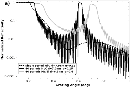
Bragg mirrors, consisting of multiple thin layers of dielectric material, can by carefull design reflect for specific wavelenghts of electromagnetic radiation. Where single layer mirrors are rather limited in that the incoming grazing angles should be below or close to the critical angle of that material, multi-layer mirrors allow for larger angle windows. Multilayered thin film mirrors efficiently reflecting X-rays, nowadays find their application towards a variety of applications such as EUV photolitography, X-ray microscopy, synchrotron radiation, plasma physics and astrophysics. For EUV photolitography working around a 13 nm wavelength, typically Mo/Si multi-layers having a reflectivity of about 60% find good use. At lower wavelenghts, however, their reflectivity becomes very low, a region where Ni/C multi-layers have higher reflectivity. Spiga et al. [1] e.g. measured a reflectivity of 95%. For current hard X-ray focusing telescopes, the use of Pt and the corresponding K adsorption edge leads to an upper energy limit of 79.4 keV. The usage of a different heavy element in the multi-layers, such as Ni, can result in an extended energy bandwidth into the soft -ray range as Ni does not have adsorption edges in the hard X-ray/soft -ray range. Especially depth-graded Ni/C multi-layers find their use in focusing optics in astronomical telescopes that aim for hard X-ray and -ray observatories with typical energies of 158 keV and 511 keV, important to study respectively the Ni decay and positron-electron annihilation in supernovae [2]. In Fig. 1 we plotted the calculated X-ray reflectivity curves at 8.05 keV versus grazing angle and versus wavelength using Fresnel equations and Henke’s optical data [3]. Calculations are shown for a single Ni/C multi-layer and a 40 pairs Ni/C multi-layer, both with a Ni film thickness of 1.2 nm and a C film thickness of 6.7 nm, as suggested for an optic design for use in hard X-ray and soft -ray astronomy applications using silicon pore optics [4]. For comparison we plotted the calculated X-ray reflectivity curves for a 40 pairs Mo/Si multi-layer of 2.76 nm Mo and 4.14 nm Si. Notice the superior reflectivity for Ni/C multi-layers at grazing angles in comparison to the Mo/Si multi-layers, see Fig. 1(a), and the vanishing reflectivity at lower wavelenghts of the Mo/Si multi-layers in comparison to the Ni/C multi-layer, see Fig. 1(b).
Designing towards shorter periodic wavelenghts, however, reduces the experimentally observed reflectivity significantly in comparison to the anticipated theoretical reflectivity. This is anticipated to result from the substantial interface roughness, caused by crystallization of Ni and is found to occur below a thickness of 2 nm followed by interdiffusion between adjacent Ni and C layers worsening the observed interlayer roughness [5, 6, 7, 8, 9]. In order to reduce the roughness between adjacent layers, Pulsed Laser Depositing (PLD) these films is found to result in smoother films as the deposited particles having higher kinetic energy of several 100 eV can smoothen the Ni/C interface.
Here, we investigate the feasibility of producing such thin multi-layers by the use of Pulsed Laser Deposition on a silicon-oxide (SiO) substrate containing a native oxide. Pulsed Laser Deposition is a well studied technique to aid in the synthesis of multicomponent and complex thin films. In comparison to conventional vapor deposition techniques, PLD provides additional parameters thereby in principle giving more flexibility to the (control of the) growth process of thin films. Besides this, PLD is known for its high supersaturation in growth, resulting in a high nucleation density resulting in (ultra)smooth thin film growth [10], a necessity for the application described before. Although a lot of work is done on the PLD growth of (complex) oxides [10], only little studies are done on the initial stages of the growth of metallic thin films [11, 12, 13, 14, 15, 16]. In this work, we study the evolution of metallic thin films grown by PLD with emphasis on the process variables. By studying the growth at varying conditions, we seek the optimal PLD growth conditions for Ni/C thin film multi-layers as well as studying the influence on the resulting reflectivity, as these multi-layers could serve as a next generation coating for application in future hard X-ray and soft -ray optics.
In this paper, we therefore start by the growth and characterization of individual Ni and C films in order to optimize the individual growth conditions. We then stack these films at elevated temperature to test their thermal stability. As analysis reveals the intermixing of Ni and C at elevated temperatures, we summarize by analysis of pairs of Ni/C multi-layers grown at RT conditions, discussing the experimentally observed reflectivity in view of the theoretically predicted one. This brings us to conclusions and outlook towards future applications.
2 Experimental details
For comparison to commercially available silicon-oxide pore optics [4], we diced a native silicon-oxide wafer in samples of 55 mm2 which were then ultrasonically degreased in acetone and ethanol prior to insertion into the vacuum setup. The SiO sample was glued by silver-paste to a sample-holder that could be heated in-situ by laser heating. The sample temperature was measured by a pyrometer at the backside of the sample-holder, estimated to result in an error of 50∘C.
A PLD system from Twente Solid State Technology (TSST) B.V. was used in combination with a 248 nm excimer laser with a pulse duration of 25 ns to ablate material from the targets: single crystal Ni(111) and Highly Oriented Pyrolytic Graphite (HOPG) of ZYA grade. A rectangular mask was used to create a well-defined and homogeneous laser profile on the target. The target was positioned 50 mm from the substrate. The laser fluence was controlled using a variable beam attenuator. By applying a magnification of 11.5, we achieved a laser energy density of 6 J/cm2 for the ablation of C and 7.5 J/cm2 for the ablation of Ni, using a spot-size of 0.6 mm2. Both were scanned during deposition over a width of 5 mm at a speed of 0.5 mm/second. The background gas pressure was in the range of 10-8 mbar.
The growth rate per pulse was obtained by determination of the Kiessig fringes in the resulting X-ray reflectivity curve for a thick film grown. For Ni we determined a growth rate of 1.910-3 nm/pulse where growth was performed at a repetition rate of 8 Hz. The growth rate for C was found to be 1.810-2 nm/pulse at a repetition rate of 10 Hz.
During deposition the surface structure was monitored using Reflective High Energy Electron Diffraction (RHEED) operated at 30 keV, at pressures up to 0.3 mbar, enabled due to differential pumping. Subsequently, X-ray reflectivity (XRR) and diffraction (XRD) at a Cu K- wavelength was used for reflectivity and structural characterization of the multi-layers. By use of ex-situ tapping mode atomic force microscopy (TM-AFM) the resulting surface roughness () was determined. The surface roughness (RMS) of the pristine SiO samples was found to be 0.58 nm.
3 Results and discussion
To study and optimize the PLD growth conditions for individual Ni and C films, typical parameters in the PLD method should be considered; the laser fluence, giving the target particles their initial kinetic energy; the laser repetition rate, dictating the growth rate; the process pressure, reducing the kinetic energy of the particles arriving on the substrate as well as the plasma shape [17]; and the substrate temperature, enhancing diffusivity during the growth. Here, we focus on the role of process pressure and substrate temperature upon growth, as they mainly govern the roughness of the resulting film as for its reflective properties of the multi-layer we are not interested in obtaining highly crystalline films.
As is described in literature for the growth of thin graphite films, an increase in laser energy density results in higher quality films [18, 19]. Besides this, a thermal treatment is known to increase the thin film quality [19, 20]. As a low surface roughness is of utmost importance for future applications, we deposited thin graphite films at the described conditions, an ablation threshold of 6 J/cm2, for increasing process pressures of respectively 0.027, 0.05 and 0.1 mbar of Ar, as an increased process pressure typically leads to more 2D growth for PLD growth [21, 22, 23, 17]. For PLD films grown at process pressures beyond 0.027 mbar, we find however a sharp increase in roughness. Therefore, the process pressure throughout this paper was 0.027 mbar of Ar by influx of a 40 standard cubic centimeter (SCCM) Ar flow and subsequent control on the pump rate by positioning the gate valve between pump and vacuum chamber.
In comparison to the PLD of oxides, the ablation of metal targets requires ablation thresholds typically an order of magnitude higher [16]. However, too large ablation thresholds in combination with a too low process pressure results in droplet formation at growth [11, 12, 13, 15, 14]. A study on the microstructural evolution of Ni films upon increasing ablation threshold [24] revealed an increased clustering and denser packing of nanoparticles. In order to obtain sufficiently high deposition rates in high vacuum, laser fluences of more than 5 J/cm2 are a necessity. Besides this, it should be noted that in order to reduce the droplet density, a sweet spot of 7-9 J/cm2 exists, as discussed in Fig. 5 of Ref. [14]. Making use of an ablation threshold of 7.5 J/cm2 and a process pressure of 0.042 mbar to reduce the kinetics of the arriving particles, we obtain low roughness Ni surfaces which show no preferential crystallographic orientation.
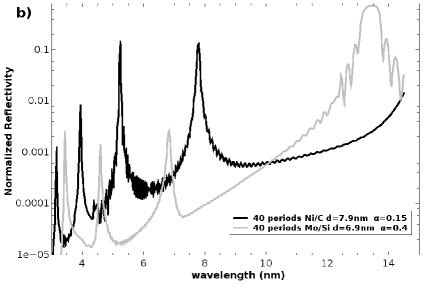
In order to study the quality of the mirror, which depends on the quality of every single layer deposited, we started by analyzing single layers of Ni and C deposited by PLD. Before deposition, the RHEED pattern reveals a clean SiO substrate pattern as shown in Fig. 2(a). Upon deposition of C at RT, a continuous decay in the intensity of the substrate spots appears. For thicker films, clear transmission RHEED patterns of multiwalled carbon nanotubes appear, see e.g. Fig. 2(b). The transmission pattern was checked by tilting the sample as well as varying the angle of incidence with respect to the surface, see Fig. 2(c-h). By this, substrate features should reveal position changes as they are very sensitive to tilt, in contrast to transmission features which keep their position.
In order to calculate the preferred interplanar distances within the C film, the preferred Debye-Scherrer ring radius is calculated by integrating the radial intensity distribution along the periphery of circles around the RHEED central spots for increasing radius. Fig. 2(i) shows the integral of the radial intensity distribution of Fig. 2(c). Similar to RHEED images described for randomly oriented multiwalled carbon nanotube samples, the radial profile of the diffraction intensity is in correspondence with graphites lattice parameters and as described in detail in Ref. [25].
For Ni films grown, we only observe a continuous decay in the RHEED intensity of the substrate spots, however, no formation of a transmission RHEED pattern. This is also the case for thicker Ni films, indicative of the amorphous microstructure of the layer, a necessity for efficient mirrors.
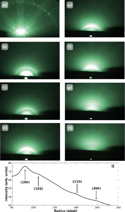
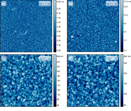
In Fig. 3(a-c), we show topographic TM-AFM images of the grown 1.2 nm thick Ni and 6.7 nm thick C films. The different AFM image sizes reveal roughnesses (RMS) 0.1-1.4 nm. In comparison to magnetron-sputtered Ni films [9], where the roughness increases for decreasing film thickness, the roughness at the interface seems rather ill defined. We should however take into account that during the PLD processing of metals, the formation of spherical droplets with sizes in the range of 0.1-0.2 m are often reported [14, 26]. From a grain analysis on the AFM images shown in Fig. 3 we find spherical droplets having similar dimensions. Although larger sized droplets can easily be avoided, these smaller droplets result from the fast heating and cooling occuring during melting of the targets surface and can not be completely avoided. Literature suggests the use of some kind of velocity filter in order to obtain droplet free films [14]. By marking these small droplets and excluding them from the analysis, we find roughnesses (RMS) in the range of 0.1-0.2 nm. If one would be able to avoid the droplets resulting from the heating and cooling at the target, one would obtain PLD films superior to magnetron-sputtered films.
For the roughness (RMS) of the C films, see Fig. 3(d-e), we find values between 0.2-0.8 nm. For these films, we observe an increased number of small droplets in line with the observations for the Ni films. Excluding the droplets from the image analysis, reveals a roughness (RMS) of 0.2 nm, in agreement with the observations for the thickness dependent roughness (RMS) of magnetron-sputtered C films [9].
| AFM image size | Ni film | C film |
|---|---|---|
| 1010m2 | 0.23nm (1.36nm) | 0.24nm (0.78nm) |
| 55m2 | 0.14nm (0.91nm) | 0.22nm (0.51nm) |
| 11m2 | 0.09nm | 0.11nm |
Having found PLD conditions to grow Ni and C films, both, with surface roughnesses 0.2 nm for the required thicknesses of respectively 1.2 and 6.7 nm, we stack both films, thereby changing the growth conditions in sequence. For the Ni film we use an ablation threshold of 7.5 J/cm2 and a substrate temperature at RT, where for the following C film we use an ablation threshold of 6 J/cm2 and vary the growth temperature as a thermal treatment is known to increase the thin film quality [19, 20] and more importantly, to test the thermal stability of the multi-layer as it is required in astronomy applications [4].
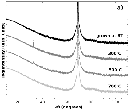
To test the thermal stability of the grown multi-layer, we followed a different approach compared to the straightforward heating of the multi-layer as described in Ref. [5]. There it is found that the reflectivity of the multi-layer is destroyed upon heating beyond 300∘C, explained by the formation of carbides which decompose upon heating at higher temperatures. Here, we want to investigate the role of substrate temperature during deposition instead of post-processed as a thermal treatment is known to increase the thin film quality [19, 20]. We therefore use a growth temperature for the C layer of RT, 300∘C, 500∘C and 700∘C. As film thicknesses of 1.2 nm (Ni) and 6.7 nm (C) are hard to measure by Cu K- X-rays as the Kiessig fringes are very wide in 2, and one typically hits the noise floor of the detector for angles beyond 5∘, we study thicker C (75 nm) and Ni (20 nm) films here, in order to make it easier to determine the Kiessig fringes and to enable for more pronounced diffusivity through the multi-layer. Characterization by X-ray diffraction and reflectivity is plotted in Fig. 4(a) and (b). In Fig. 4(a) we plot the X-ray diffraction curve for a multi-layer grown at RT. The pattern reveals no specific crystallographic preferential orientation for Ni(111) at 44.6∘ [27], Ni(200) at 51.8∘ or Ni(220) at 76.4∘ in agreement with JCPDS No:04-0850. Similar, the X-ray diffraction pattern shows no preferential crystallographic orientation for a crystalline C film, known to result in a weak and broad peak around 20∘ [18, 28]. The peak at 33∘ and 69∘ corresponds to the silicon wafer, used as a substrate. In contrast to Ref. [5], we do not observe any indication for crystalline Ni(111) nor Ni(200) formation in our curves, although the layers of the multi-layer described here are thicker and the effect is therefore expected to be more pronounced.
The diffraction patterns, see Fig. 4(a), do not show any formation of carbides (Ni3C) nor highly crystalline Ni structures as compared to Ref. [5]. From the bulk phase diagram [29], these nickel carbide structures are anticipated to appear in a narrow temperature window [5], depending on the Ni/C ratio at the interface. As the temperature reading used in our experiments might be underestimated, we might have been beyond this temperature window, resulting in the lack of nickel carbide structures.
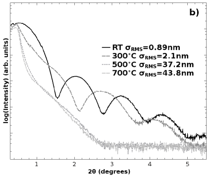
In Fig. 4(b) we plot the corresponding X-ray reflectivity curves, revealing clear Kiessig fringes, arising from the constructive interference between the X-rays reflected from the film-vacuum, film-film and substrate-film interface. We find the reflectivity to be fully destroyed upon growth temperatures beyond 300∘C as can be seen by the absence of Kiessig fringes in Fig. 4(b), indicative of ill defined interfaces at the film-vacuum, film-film and substrate-film interface in agreement with literature [5]. Obviously this is undesired for the application in mind. Note that the critical angle decreases at increased growth temperature for the C layer, indicative of a decrease of the density of the multi-layer by about 25%. Besides this, the periodicity of the Kiessig fringes is also shifting at 300∘C, suggesting C segregation into Ni described in literature. Partial segregation of the Ni would decrease the thickness of the reflective Ni layer, resulting in an increase in the width of the Kiessig fringes as observed here. This is hinting towards shifting of the interface between the C and Ni film, towards deeper depth. To investigate the several interfaces in more detail and study the cause for the destroyed reflectivity at growth temperatures beyond 300∘C, we make use of additional experimental techniques.
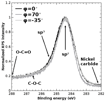
To confirm the lack of nickel carbide formation at elevated temperature, we probed the surface chemical properties by depth-profiling X-ray photoelectron spectroscopy (XPS), see Fig. 5. By variation of the angle of incidence, the estimated penetration depth is about 10 nm at (for perpendicular incidence), 7 nm at and 3 nm at incidence with respect to the substrates normal. The C 1s peak shows omnipresent contributions of the carbon and peaks at respectively 284.5 eV and 285.4 eV for all angles of incidence where the high ratio of : is indicative for amorphous carbon [30]. Nickel carbides, found around 282.8 eV [31], show only a faint signature when probing more surface sensitive. The COC and OCO functional groups at respectively 286.5 eV and 288.7 eV seem absent as this film has been prepared and transferred to XPS in (ultra)high vacuum conditions.
As the loss of reflectivity can result from an ill defined film-vacuum, film-film and/or substrate-film interface, we investigate the film-vacuum surface morphology by AFM, see Fig. 6(a-d). The measured surface roughness (RMS) by AFM for C films grown at RT is 0.89 nm, see Fig. 6. For increasing growth temperature, the roughness (RMS) increases to 2.1 nm at 300∘C, 37.6 nm at 500∘C and 45 nm at 700∘C. Krawietz et al. [5] attribute the change in reflectivity beyond 300∘C solely to the fragmentation of the Ni layers supported by the outdiffusion of C from the Ni layers.
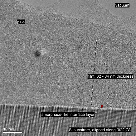
In order to investigate the different interfaces, we grow a multi-layer of 5 Ni/C stacks containing a 1.2 nm thick Ni layer followed by a 6.7 nm thick C layer, where the Ni layer was grown at RT and the C layer was grown at 700∘C. This sample was then perpendicular cut and grinded carefully to a thickness where XTEM could be performed. The resulting XTEM image is shown in Fig. 7. At the bottom of the image, the highly crystalline Si substrate is imaged along the [022]-axis. Above the Si substrate, a thin amorphous oxide layer can be discriminated. Above this, we find a thick layer of 32-34 nm in thickness, in good agreement with the deposited amount of Ni and C material. In this thick layer, we can not discriminate individual Ni and C layers. Instead, a layer of randomly oriented carbon nanotubes can be seen, with intermixed in it, crystalline clumps of Ni, similar to as described in Ref. [9]. The crystalline Ni clumps, having sizes up to 4-5 nm in diameter, suggest outdiffusion of C [5].
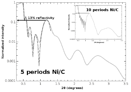
To study the feasibility of creating high reflectivity multi-layers by PLD growth, we investigate the resulting reflectivity of several pairs of multi-layers grown. As the growth of multi-layers at elevated temperatures results in intermixing of Ni and C destroying its reflective properties, we summarize this paper by growing a 5 and 10 pairs Ni/C multi-layer at RT, both with a Ni film thickness of 1.2 nm and a C film thickness of 6.7 nm at the same laser energy densities and process pressures described before. In Fig. 8 we plot the X-ray reflectivity curve for 5 pairs of Ni/C multi-layers. For 10 pairs of Ni/C multi-layers, see inset of Fig. 8.
From calculated X-ray reflectivity curves at 8.05 keV the resulting reflectivity at a grazing angle of =0.6∘ is 13.9% for 5 pairs increasing to 42.6% for 10 pairs of multi-layers. An increase of the number of pairs of multi-layers results into an increased reflectivity at this grazing angle, see also Fig. 1(a). Analyzing the experimentally grown pairs of multi-layers in Fig. 8(a) and (b), we find a reflectivity for the 5 and 10 pairs of respectively 13.0% and 11.8%. Note that the reflectivity for 5 pairs of multi-layers is close to the theoretically predicted value, whereas for an increasing number of pairs the reflectivity does not increase. In order to understand this, we quantify the roughness for the film-vacuum and substrate-film interface, by modeling the system as film pairs of uniform (electronic) density on top of a uniform (electronic) dense substrate. Fitting was done by using the fitting parameters film thickness ( and ), assuming constant thicknesses for all layers, interface roughness between Ni () and C films () and Ni-substrate interface roughness (), a background resulting from scattering and a normalization factor [32]. Note that we fit up to limited 2 angle (see the dashed line in Fig. 8) to ensure the dynamical scattering theory is applicable and stay far from the kinetical scattering regime [33, 34]. From this we find a steep roughness increase going from 5 pairs (=0.27 nm and =0.41 nm) to 10 pairs of Ni/C multi-layers (=1.3 nm and =2.1 nm) grown by PLD at RT. Note that for 5 pairs, the fitted roughnesses agree well with the studied AFM images, see also Fig. 3. For 10 pairs of multi-layers, the roughness of samples grown at RT appears to be dictated by the droplets as discussed in Table 1.
4 Conclusions
Here, we investigated the PLD grown low roughness Ni/C multi-layers by use of RHEED, XRD, XRR, TM-AFM, XPS and XTEM. Thin Ni and C layers with roughnesses below 0.2 nm can be created by PLD at RT. However, due to the fast heating and cooling occuring during melting of the targets surface, small droplets during deposition can not be avoided limiting the reflectivity at grazing angles for increased number of pairs of multi-layers. Growth at temperatures of about 300∘C results in intermixing of Ni and C, destroying the reflective properties of the multi-layer. XTEM image analysis of multi-layers grown at elevated temperatures reveals (crystalline) Ni clumps intermixed with C. For future applications in hard X-ray and soft -ray focusing telescopes, the stability of multi-layers under extreme (temperature) conditions is required and needs further investigation in order to find technological solutions.
5 Acknowledgments
This work is part of the research programme of NanoNext NL project 7B Multilayered and artificial materials, project 12 and the research programme of the Foundation for Fundamental Research on Matter (FOM), which is part of the Netherlands Organisation for Scientific Research (NWO). Cross-section TEM imaging has been performed by Dr. Rico Keim. The author is gratefull to Prof. Dr. Ing. G. Rijnders for his permanent support.
6 References
References
- [1] D. Spiga, G. Pareschi, G. Grisoni, G. Valsecchi, Hard x-ray multilayer coated astronomical mirrors by e-beam deposition (2004).
- [2] E.-J. Buis, M. Beijersbergen, G. Vacanti, M. Bavdaz, D. Lumb, Design aspects of grazing angle multilayer mirrors for soft gamma-rays, Springer Netherlands, Dordrecht, 2006, pp. 105–113.
- [3] B. L. Henke, J. C. Davis, E. M. Gullikson, R. C. C. Perera, A preliminary report on x-ray photoabsorption coefficients and atomic scattering factors for 92 elements in the 10-10.000 ev region, Report Number: LBL-26259 - (1988) –.
- [4] M. J. Collon, G. Vacanti, R. Günther, A. Yanson, N. Barriere, B. Landgraf, M. Vervest, A. Chatbi, R. van der Hoeven, M. W. Beijersbergen, M. Bavdaz, E. Wille, B. Shortt, J. Haneveld, A. Koelewijn, C. van Baren, A. Eigenraam, P. Müller, M. Krumrey, V. Burwitz, G. Pareschi, P. Conconi, S. Massahi, F. E. Christensen, G. Valsecchi, Silicon pore optics for the athena telescope (2016).
- [5] R. Krawietz, B. Wehner, D. M. andK. Richter, H. Mai, R. Dietsch, S. Hopfe, R. Scholz, W. Pompe, Investigation of the thermal stability of ni/c multilayers by x-ray methods, Fresenius J Anal Chem 353 (1995) 246–250.
- [6] H. Takenaka, T. Kawamura, H. Kinoshita, Fabrication and evaluation of ni/c multilayer soft x-ray mirrors, Thin Solid Films 288 (1996) 99–102.
- [7] R. Dietsch, T. Holz, H. Mai, C.-F. Meyer, R. Scholz, B. Wehner, High precision large area pld of x-ray optical multilayers, Applied Surface Science 127 (1998) 451 – 456.
- [8] G. Georgescu, V. Nelea, M. Ulmeanu, C. Ghica, N. Nastase, Growth of carbon/nickel multilayer for x-ray-uv optics by rf reactive magnetron sputtering, Applied Surface Science 148 (3) (1999) 142 – 146.
- [9] J. Peng, W. Li, Q. Huang, Z. Wang, Microstructure evolution with varied layer thickness in magnetron-sputtered ni/c multilayer films, Scientif Reports 6 (2016) 31522.
- [10] D. H. A. Blank, M. Dekkers, G. Rijnders, Pulsed laser deposition in twente: from research tool towards industrial deposition, Journal of Physics D: Applied Physics 47 (3) (2014) 034006.
- [11] H.-U. Krebs, O. Bremert, Pulsed laser deposition of thin metallic alloys, Applied Physics Letters 62 (19) (1993) 2341–2343.
- [12] H.-U. Krebs, O. Bremert, M. Störmer, Y. Luo, Comparison of the structure of laser deposited and sputtered metallic alloys, Applied Surface Science 86 (1-4) (1995) 90 – 94.
- [13] J. G. Lunney, Pulsed laser deposition of metal and metal multilayer films, Applied Surface Science 86 (1995) 79–85.
- [14] S. Fähler, M. Störmer, H. Krebs, Origin and avoidance of droplets during laser ablation of metals, Applied Surface Science 109-110 (0) (1997) 433 – 436.
- [15] H. Krebs, M. Störmer, S. Fähler, O. Bremert, M. Hamp, A. Pundt, H. Teichler, W. Blum, T. Metzger, Structural properties of laser deposited metallic alloys and multilayers, Applied Surface Science 109-110 (0) (1997) 563 – 569.
- [16] L. Doeswijk, G. Rijnders, D. Blank, Pulsed laser deposition: metal versus oxide ablation, Applied Physics A 78 (3) (2004) 263–268.
- [17] R. Groenen, J. Smit, K. Orsel, A. Vailionis, B. Bastiaens, M. Huijben, K. Boller, G. Rijnders, G. Koster, Research update: Stoichiometry controlled oxide thin film growth by pulsed laser deposition, APL Materials 3 (7) (2015) 070701.
- [18] S. R. Sarath Kumar, P. K. Nayak, M. N. Hedhili, M. A. Khan, H. N. Alshareef, In situ growth of p and n-type graphene thin films and diodes by pulsed laser deposition, Applied Physics Letters 103 (19) (2013) 192109.
- [19] S. R. Sarath Kumar, H. N. Alshareef, Ultraviolet laser deposition of graphene thin films without catalytic layers, Applied Physics Letters 102 (1) (2013) 012110.
- [20] T. Tite, C. Donnet, A.-S. Loir, S. Reynaud, J.-Y. Michalon, F. Vocanson, F. Garrelie, Graphene-based textured surface by pulsed laser deposition as a robust platform for surface enhanced raman scattering applications, Applied Physics Letters 104 (4) (2014) 041912.
- [21] K. Sturm, S. Fähler, H.-U. Krebs, Pulsed laser deposition of metals in low pressure inert gas, Applied Surface Science 154-155 (0) (2000) 462 – 466.
- [22] T. Scharf, H. Krebs, Influence of inert gas pressure on deposition rate during pulsed laser deposition, Applied Physics A 75 (5) (2002) 551–554.
- [23] T. Scharf, J. Faupel, K. Sturm, H.-U. Krebs, Pulsed laser deposition of metals in various inert gas atmospheres, Applied Physics A 79 (4-6) (2004) 1587–1589.
- [24] P. Kumar, M. G. Krishna, A. Bhatnagar, A. Bhattacharya, Dynamic force microscopy study of the microstructural evolution of pulsed laser deposited ultrathin ni and ag films, Journal of Materials Research 23 (2008) 1826–1839.
- [25] J. Drotar, B. Wei, Y.-P. Zhao, G. Ramanath, P. Ajayan, T.-M. Lu, G.-C. Wang, Reflection high-energy electron diffraction from carbon nanotubes, Phys. Rev. B 64 (2001) 125417.
- [26] A. Largeanu, G. Pompilian, D. Galusca, M. Agop, S. Gurlui, Pulsed laser deposition of ni thin films on metallic substrate, U.P.B. Sci. Bull., Series A 73 (2011) 195–202.
- [27] D. L. Miller, M. W. Keller, J. M. Shaw, A. N. Chiaramonti, R. R. Keller, Epitaxial (111) films of cu, ni, and cuxniy on a-al2o3 (0001) for graphene growth by chemical vapor deposition, Journal of Applied Physics 112 (6) (2012) 064317.
- [28] A. Ruammaitree, H. Nakahara, K. Akimoto, K. Soda, Y. Saito, Determination of non-uniform graphene thickness on sic (0001) by x-ray diffraction, Applied Surface Science 282 (2013) 297 – 301.
- [29] M. Singleton, P. Nash, The c-ni (carbon-nickel) system, Bull. Alloy Phase Diagrams 10 (1989) 121–126.
- [30] J. Lascovich, R. Giorgi, S. Scaglione, Evaluation of the sp2/sp3 ratio in amorphous carbon structure by xps and xaes, Applied Surface Science 47 (1) (1991) 17 – 21.
- [31] D. H. Seo, S. Pineda, J. Fang, Y. Gozukara, S. Yick, A. Bendavid, S. K. H. Lam, A. T. Murdock, A. B. Murphy, Z. J. Han, K. K. Ostrikov, Single-step ambient-air synthesis of graphene from renewable precursors as electrochemical genosensor, Nature Communications 8 (2017) 14217.
- [32] M. Björck, G. Andersson, GenX: an extensible X-ray reflectivity refinement program utilizing differential evolution, J. Appl. Crystallogr. 40 (2007) 1174–1178.
- [33] M. Jankowski, D. Kami?ski, K. Vergeer, M. Mirolo, F. Carla, G. Rijnders, T. R. J. Bollmann, Controlling the growth of bi(110) and bi(111) films on an insulating substrate, Nanotechnology 28 (15) (2017) 155602.
- [34] E. Vlieg, Surface and Interface Science, Volumes 1 and 2: Volume 1 - Concepts and Methods, Wiley-VCH, 2012.