Effective surface conductivity of plasmonic metasurfaces: from far-field characterization to surface wave analysis
Abstract
Metasurfaces offer great potential to control near- and far-fields through engineering of optical properties of elementary cells or meta-atoms. Such perspective opens a route to efficient manipulation of the optical signals both at nanoscale and in photonics applications. In this paper we show that by using an effective surface conductivity tensor it is possible to unambigiously describe optical properties of an anisotropic metasurface in the far- and near-field regimes. We begin with retrieving the effective surface conductivity tensor from the comparative analysis of experimental and numerical reflectance spectra of a metasurface composed of elliptical gold nanoparticles. Afterwards restored conductivities are validated in the crosscheck versus semianalytic parameters obtained with the discrete dipole model with and without dipoles interaction contribution. The obtained effective parameters are further used for the dispersion analysis of surface plasmons localized at the metasurface. The effective medium model predicts existence of both TE- and TM-polarized plasmons in a wide range of optical frequencies and describes peculiarities of their dispersion, in particularly, topological transition from the elliptical to hyperbolic regime with eligible accuracy. The analysis in question offers a simple practical way to describe properties of metasurfaces including ones in the near-field zone by extracting effective parameters from the convenient far-field characterisation.
DTU Fotonik, Technical University of Denmark, Oersteds pl. 343, DK-2800 Kongens Lyngby, Denmark
1 Introduction
Miniaturization of integrated optical circuits requires an effective control of light on the subwavelength scale. Significant advances in this field have been achieved with the help of metamaterials 1, 2, 3 – artificially created media, whose electromagnetic properties can drastically differ from the properties of the natural materials. However, a three-dimensional structure of metamaterials, related fabrication challengers and high costs, especially for optical applications, form significant obstacles in their implementation in integrated optical circuits.
An alternative way is to use metasurfaces – two-dimensional analogues of metamaterials. There are also natural two-dimensional anisotropic materials such as hexagonal boron nitride 4, 5, transition metal dichalcogenides 6, 7, black phosphorus 8. In the visible and the near-IR range, metasurfaces can be implemented using subwavelength periodic arrays of plasmonic or high-index dielectric nanoparticles 9, 10, 11. A nanostructured graphene could also be considered as a metasurface for THz frequencies 12, 13. In the microwave range, metasurfaces can be implemented by using LC-circuits, split-ring resonators, arrays of capacitive and inductive elements (strips, grids, mushrooms), wire medium etc 14, 15. Despite subwavelength or even monoatomic thicknesses, the metasurfaces offer unprecedented control over light propagation, reflection and refraction 14, 16.
Metasurfaces exhibit a lot of intriguing properties for a wide area of applications such as near-field microscopy, imaging, holography, biosensing, photovoltaics etc 14, 9, 16, 15. For instance, it was shown that metasurfaces based on Si nanoparticles can exhibit nearly 100% reflectance 17 and transmittance 18 in a broadband frequency range. Moreover, metasurfaces can serve as light control elements: frequency selectors, antennas, lenses, perfect absorbers 15. They offer an excellent functionality with polarization conversion, beam shaping and optical vortices generation 19, 20. Besides, metasurfaces provide an efficient control over dispersion and polarization of surface waves 21, 22, 9, 23, 24, 25. Surface plasmon-polaritons propagating along a metasurface assist pushing, pulling and lateral optical forces in its vicinity 26, 27. Metasurfaces are prospective tools for spin-controlled optical phenomena 28, 29, 30, 31 and holographic applications 32, 33, 34. The main advantages of metasurfaces, such as relative manufacturing simplicity, rich functionality and planar geometry, fully compatible with modern fabrication technologies, create a promising platform for the photonic metadevices. It has been recently pointed out that all-dielectric metasurfaces and metamaterials can serve as a prospective low loss platform, which could replace plasmonic structures 35. However, one of the main advantages of plasmonic structures unachievable with dielectric ones is that the plasmonic structures can be resonant in the visible range keeping at the same time a deep subwavelength thickness and period. Thus, here we concentrate on plasmonic metasurfaces allowing light manipulation with a deep subwavelength structure.
The common feature of bulk metamaterials and metasurfaces is that due to the subwavelength structure they can be considered as homogenized media described by effective material parameters. For bulk metamaterials, such effective parameters are permittivity and/or permeability . Retrieving effective parameters is one of the most important problems in the study of metamaterials. Generally, the effective parameters are tensorial functions of frequency , wavevector , and intensity . Homogenization of micro- and nanostructured metamaterials can become rather cumbersome, especially taking into account nonlocality 36, 37, chirality 38, bi-anisotropy 39, 40 and nonlinearity 41, 42.
Analogous homogenization procedures are relevant for metasurfaces. Apparently, homogenization procedures for 2D structures were firstly developed in radiophysics and microwaves (equivalent surface impedance) in applications to thin films, high-impedance surfaces and wire grids etc 43, 44, 45. It has been recently pointed out that two-dimensional structures, like graphene, silicene and metasurfaces, can be described within an effective conductivity approach 46, 47, 23, 48, 24, 49. In virtue of a subwavelength thickness, a metasurface could be considered as a two-dimensional equvalent current and, therefore, characterized by effective electric and magnetic surface conductivity tensors, where is the component of the wavevector in the plane of the metasurface 14, 15. Importantly, such effective surface conductivity describes the properties of the metasurface both in the far-field when (reflection, absorption, refraction, polarization transformation etc.) and in the near-field (surface waves, Purcell effect, optical forces), when .
In this paper, we focus our study on a resonant plasmonic anisotropic metasurface represented by a two-dimensional periodic array of gold nanodisks with the elliptical base. We derive and analyze the electric surface conductivity tensor of the anisotropic metasurface in three ways: (i) theoretically by using the discrete dipole model; (ii) experimentally by characterization of the metasurface reflection spectra and (iii) numerically by combining the optical measurements of the fabricated metasurface, simulations of the experiment and analytical approach (zero-thickness approximation). We reveal that the effective surface conductivity tensor extracted from the far-field measurements well describes near-field properties of metasurface such as the spectrum of surface waves and their behaviour in all possible regimes - capacitive, inductive, and hyperbolic. By using the discrete dipole model we study the effects of spatial dispersion on the eigenmodes spectrum and define the limitations of the effective model applicability.
2 Sample Design and Fabrication
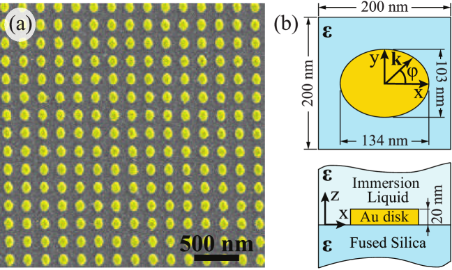
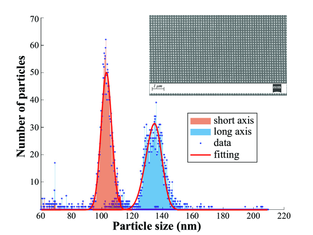
We consider a metasurface composed of gold anisotropic nanoparticles placed on a fused silica substrate. The design of the sample is shown in Fig. 1. The target structure consists of 20 nm thick gold nanodisks with the elliptical base packed in the square lattice with a period of 200 nm. The average long and short axes of the disks are nm and nm, respectively. The distribution of the nanodisks sizes is provided in Fig. 6 (See Supporting Information).
The sample was fabricated via electron beam lithography on a fused silica substrate. Before the electron beam exposure process, the resist layer (PMMA) was covered with a thin gold layer to prevent local charge accumulation. After the exposure, a 20 nm thick gold layer was sputtered via thermal evaporation. During the last step of the fabrication process, the remains of the resist were removed via the lift-off procedure. Finally, the sample was immersed in a liquid with a refractive index nearly matching the glass substrate. Thus, we obtained the metasurface with a homogeneous ambient medium with permittivity . The SEM image of the fabricated sample is shown in Fig. 1a.
3 Effective Conductivity Tensor
The plasmonic resonant metasurface shown in Fig. 1 is anisotropic and non-chiral. Asymmetry of each particle splits its in-plane dipole plasmonic resonance with frequency into two resonances with frequencies and 23, 50. Consideration of metasurfaces as an absolutely flat object might be restricted due to the emergence of the out-of-plane polarizability caused by the finite thickness of the plasmonic particles. In our case, the out-of-plane polarizability is neglected due to a small thickness of the particles as it is shown in Fig. 7 (See Supporting Information). Therefore, this metasurface can be described by a two-dimensional effective surface conductivity tensor diagonal in the principal axes (when the axes of coordinates systems are parallel to the axes of the elliptical base of the nanodisks).
3.1 Zero-thickness Approximation
To extract the effective surface conductivity of the fabricated sample, we apply a procedure based on the combination of the optical experiments, numerical simulations and theoretical calculations.
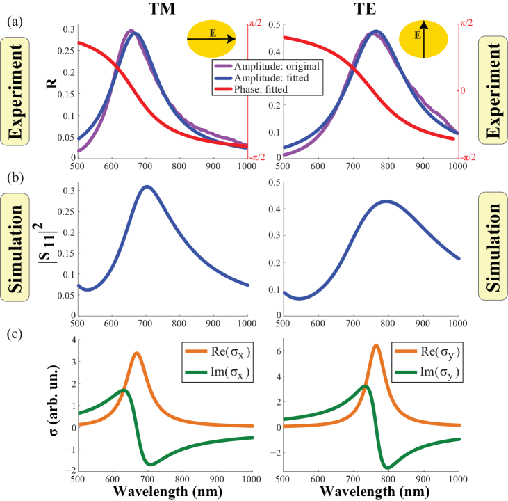
First, we measure the intensity of the reflectance for the light polarized along and across the principle axes of the metasurface under normal incidence (Fig. 2a). Both spectra demonstrate single peaks corresponding to the individual localized plasmon resonances of the nanodisks. The phase retrieved by the fitting of the experimental reflectance with the intensity calculated by the use of the Drude formula (See Supporting Information) is shown in Fig. 2a by the red lines.
Then, we model the experiment with CST Microwave Studio (Fig. 2b). The difference in the intensity of the peaks in Figs. 2a and 2b can be attributed to roughness and inhomogeneity of the sample. To equalize the measured and simulated peak values We increase the imaginary part of the gold permittivity in the simulations (See Supporting Information). Retrieving the complex conductivity tensor is done by applying the intensity and phase of the modeled reflectance, wherein we obtain a good matching between the simulated and experimental shapes of the reflectance spectra (Figs. 2a and 2b).
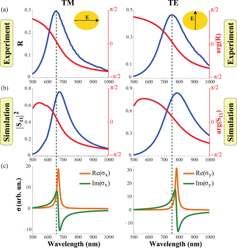
Basing on the calculated complex reflection coefficient we find an effective surface conductivity using the zero-thickness approximation (ZTA). Within this approximation we replace the real structure of finite thickness by the effective two-dimensional plane disposed at distance from the substrate. This technique can be applied only for deeply subwavelength structures. The limitation can be formulated as according to the Nicholson-Ross-Weir method 51, 52.
Considering a two-dimensional layer with effective conductivity sandwiched between two media with refractive indices (superstrate) and (substrate) one can find Fresnel’s coefficients 46, 53 and express the effective surface conductivity as follows
| (1) |
where is the component of the -matrix. Indices correspond to different orientations of the electric field of the incident wave. Hereinafter we use the Gauss system of units and express surface conductivity in the dimensionless units .
In order to obtain the proper conductivity of a metasurface one should retain only the phase of the reflection coefficient related to the metasurface properties. In the simulation, the total phase of the -parameters has two contributions . The first one arises directly when the wave reflects from the metasurface. The second phase arises because of the wave propagation from the port to the metasurface and back iiiThe time dependence is defined through the factor .. Here , is the distance between the excitation port and the metasurface. The problem is how to correctly determine distance if the metasurface has a finite thickness? We found that the correct results not breaking the energy conservation law (see Supporting Information) are obtained only if is defined as the distance to the middle of the metasurface. Thus, the effective two-dimensional layer has to be disposed exactly at distance from the substrate. The obvious analogue of ZTA is the transfer matrix method (TMM), which originates from Fresnel’s reflection and transmission coefficients. For the metasurface under consideration ZTA and TMM give the results with the average relative error of 1%. However, the advantage of ZTA over TMM is that it is necessary to know only one either reflection or transmission coefficient to extract the effective parameters.
Extracted conductivities for both polarizations are presented in Fig. 2c. For the light wave polarized along the long axis (TM-polarization) the plasmon resonance is observed at 670 nm, while for light polarized along the short axis (TE-polarization) the resonance corresponds to 780 nm.
3.2 Discrete Dipole Model
In order to derive surface conductivity of a metasurface analytically we apply the discrete dipole model (DDM)iiiiiiIn many works it is also called the point-dipole model.. This technique has been implemented for 1D, 2D and 3D structures 54, 55, 56, 57, 58. Within this approach we consider a 2D periodic array of the identical scatterers as an array of point dipoles.
In the framework of the DDM it is more convenient to operate with an effective polarizability of the structure, which is straightforwardly connected to the effective conductivity tensor as follows:
| (2) |
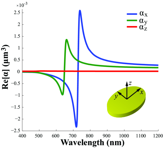
In the case under consideration, the thickness of the scatterers is deeply subwavelength and, therefore, we can neglect the polarizability of the particles in the direction perpendicular to the plane of the metasurface. Thus, we can describe the metasurface by either two-dimensional polarizability tensor or conductivity tensor with zero off-diagonal components (in the basis of the principal axes). Rigorous derivation of the effective polarizability of a two-dimensional lattice of resonant scatterers is performed in Refs. 59, 40, 56. The effective polarizability of the metasurface can be written as
| (3) |
Here, is the polarizability of the individual resonant scatterer, and is the so-called dynamic interaction constant 56. The latter contains the lattice sum, which takes into account interaction of each dipole with all others. We approximate the polarizability of the disk with the elliptical base by the polarizability of an ellipsoid with the same volume and aspect ratio (See Supporting Information). We calculate the interaction between the identical scatterers by using the Green’s function formalism:
| (4) |
Here is the dyadic Green’s function and are the coordinates of the dipoles. This sum has slow convergence. So, we calculate the interaction term in Eq. (4) within the Ewald summation technique 54, 60, 61, 57 applied for a two-dimensional periodic structure, which ensures fast convergence of the sum (See Supporting Information).
The discrete dipole model can be successfully applied for many types of metasurfaces. It is applicable for two-dimensional periodic structures under three main conditions:
-
1.
Quasistatic condition: . Here is the refractive index of the environment, is the lattice constant, is the incident wavelength.
-
2.
Dipole approximation: (or , where is the characteristic size of a scaterrer). Here is the filling factor, is the area occupied by the scatterer in the unit cell (in our case, ), is the area of the square unit cell. When the scatterers are not sufficiently small one has to take into account higher order multipoles.
-
3.
Quasi-two-dimensionality: and . This condition is achieved, when thickness of a metasurface is less than both characteristic in-plane sizes of meta-atoms () and skin depth ().
For the metasurface sample under consideration , and . Although the applicability condition of the dipole approximation is poorly satisfied, the DDM gives eligible results. Parameters and lie in the interval from 0.25 to 0.75 and from 0.02 to 0.05, respectively, for wavelengths nm. Skin depth for gold is around 20-40 nm in the wavelength range under consideration 62.
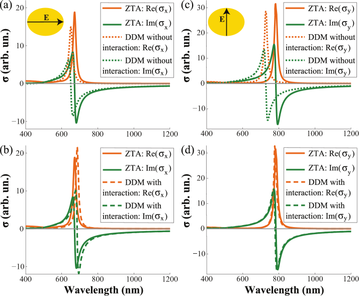
One can see in Figs. 3a and 3c that neglecting interaction term in Eq. (3) results in a blue shift of the conductivity spectra by several tens of nanometers for both polarizations. Accounting these interactions brings the DDM into almost perfect agreement with the ZTA (Figs. 3b and 3d). However, matching for is better than for . It could be explained by the fact that polarizability of an ellipsoid approximates polarizability of the elliptical disk in the direction better that in the direction.
3.3 Analysis
The spectral dependences of the extracted surface conductivities along the principal axes are shown in Fig. 2c and Fig. 3. They clearly show that the fabricated metasurface is characterized by a highly anisotropic resonant conductivity tensor:
| (5) |
One can see from Fig. 2c that the metasurface supports three different regimes depending on wavelength of the incident light. These regimes can be classified by the signs of (i) and (ii) . Specifically, when and (for 670 nm) the inductive regime of the metasurface is observed. In this case, the metasurface corresponds to the conventional metal sheet and only a TM-polarized surface wave can propagate. For and (for 780 nm) the capacitive regime of the metasurface is met, so only a TE-polarized surface wave can propagate. When (between the resonances, i.e. for wavelengths from 670 to 780 nm), a metasurface supports the so-called hyperbolic regime, in which simultaneous propagation of both TE- and TM-modes is possible 23.
4 Surface Waves
In this Section, we analyze the spectrum of the surface waves supported by the metasurface using the extracted effective conductivity tensor and compare the results with full-wave numerical simulations.
The dispersion equation of the surface waves supported by an anisotropic metasurface, described by the effective conductivity tensor (5), can be straightforwardly derived from Maxwell’s equations and boundary conditions at the metasurface 23:
| (6) |
Here, are the tensor components in the coordinate system rotated by angle (see Fig. 1b), and are the permittivity, permeability and inverse penetration depths of the wave in the superstrate and substrate, respectively. The latter are defined as , where is the wavevector in the plane of the metasurface. In our case Eq. (6) is simplified since we consider the metasurface in non-magnetic () and homogeneous environment with the permittivity corresponding to fused silica .
The first and the second factors in the left side of Eq. (6) correspond to the dispersion of purely TE-polarized and TM-polarized surface waves, respectively. The right side of Eq. (6) is the coupling factor responsible for the mixing of TE and TM modes. If an electromagnetic wave propagates along a principal axis the coupling factor is zero, so either a conventional TM-plasmon or TE-plasmon exists. However, due to anisotropy () the coupling factor can become non-zero giving rise to hybrid surface waves of mixed TE-TM polarizations. Despite the hybridization, only one type of polarization is predominant for each mode. Therefore, it is logical to refer to such modes as quasi-TM and quasi-TE surface plasmons.
It is important to note that for a number of practical problems it is necessary to take into account nonlocal effects caused by spatial dispersion. Unfortunately, it can not be accounted for in the framework of the effective surface conductivity extracted from the normal incidence measurements. However, it can be calculated by using lattice sums. In this case, the dispersion equation for the eigenmodes has the following form:
| (7) |
Equation (7) can be transformed into Eq. (6) under the assumption that .
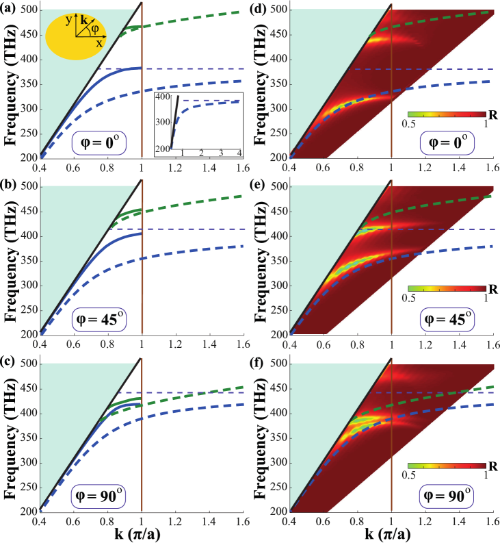
Figure 4 shows the dispersion of the surface waves localized at the studied metasurface sample for different propagation angles . In Figs. 4a-4c we compare the effective model and the discrete dipole model taking into account spatial dispersion (). One can see that the difference in the dispersions obtained within the local and nonlocal models is significant. It can be explained by quite a large filling factor , which sharply limits the accounting for nonlocal effects in the framework of the discrete dipole model. Nevertheless, both models are qualitatively similar. For instance, the resonant frequencies are close in both models for all propagation angles. Both models predict the frequency gap between TM- and TE-plasmons for which shrinks with increasing of . At , the gap disappears and both surface modes can propagate at the same frequency, that is in accordance with the results of full-wave numerical simulations (see Fig. 4f). Better matching between the results of DDM and full-wave simulations could be obtained if we account for anisotropy of the dynamic interaction constant, but this theoretical extension is the subject of our further research.
To check the applicability of the effective conductivities extracted from the far-field measurements in characterization of the near-field phenomena, we compare dispersion of the surface waves from Figs. 4a-4c with the results from full-wave numerical simulations carried out in COMSOL Multiphysics (Figs. 4d-4e). One can see good correspondence of bands at low frequencies (for the quasi-TE mode). At high frequencies, i.e. small wavelengths, the effective model works worse but it is still eligible for qualitative results.
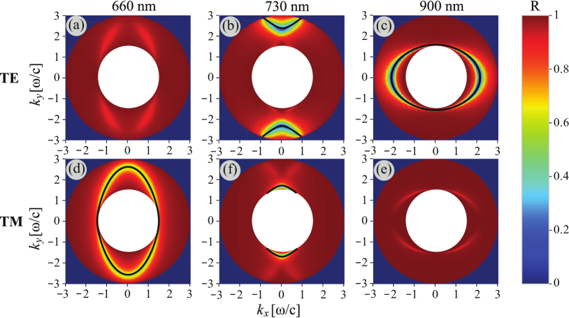
It is convenient to present dispersion of surface waves in terms of equal frequency contours, which can be visualized in reflection experiments with a high index prism (Otto geometry). We calculate reflection of a light wave in such configuration by the transfer matrix method 63. When , the equal frequency contours have an elliptic shape (Figs. 5a, 5c, 5d, 5e). For a hyperbolic regime, when ( nm), the equal frequency contours represent a set of hyperbolas for the quasi-TE mode (Fig. 5b) and arcs for the quasi-TM mode (Fig. 5f). This drastic change of the shape is often called topological transition. One can see that in the hyperbolic regime both quasi-TE and quasi-TM modes are present, i.e. simultaneous propagation of two types of surface plasmons is observed (Figs. 5b and 5f), which is consistent with bands dispersion in Fig. 4c and 4f. For the capacitive and inductive regimes only a single mode propagates. However, each mode has hybrid TE-TM polarization, so it is observed in both polarizations as shown in Fig. 5. Although polarization of the surface mode at 660 nm is predominantly similar to polarization of a conventional TM-plasmon (Fig. 5d), TE-polarization is also visible (Fig. 5a). The opposite situation takes place for a quasi-TE plasmon at nm (Figs. 5c and 5e). The exceptions are the principal axes directions where polarization of surface modes is strictly either purely TE or purely TM due to the lack of anisotropy.
5 Conclusions
To conclude, we have suggested a practical concept to describe the full set of optical properties of a metasurface. Our approach is based on extraction of the effective surface conductivity. It allows to study various phenomena in the far-field as well as to calculate the spectrum of surface waves. We have developed two techniques to retrieve the effective conductivity and discussed their limitations. There are three different regimes of the local diagonal conductivity tensor of the anisotropic metasurface composed of elliptical gold nanodisks: inductive (metal-like), capacitive (dielectric-like) and hyperbolic (like in an indefinite medium). In contrast to an isotropic metasurface such anisotropic metasurface supports two modes of hybrid polarizations. We have shown the influence of non-locality on dispersion of the surface waves. Finally, we have demonstrated the topological transition of the equal frequency contours and the hybridization of two eigenmodes. We believe these results will be highly useful for a plethora of metasurfaces applications in nanophotonics, plasmonics, sensing and opto-electronics.
This work was partially supported by the Villum Fonden, Denmark through the DarkSILD project (No. 11116), the the Ministry of Education and Science of the Russian Federation (3.1668.2017/4.6), RFBR (17-02-01234, 16-37-60064, 16-32-60123) and the Grant of the President of the Russian Federation (MK-403.2018.2). O.Y. acknowledges the support of the Foundation for the Advancement of Theoretical Physics and Mathematics “BASIS” (No 17-15-604-1).
6 Distribution of nanodisks sizes
The fabrication of a metasurface is still challenged and complicated technological process. Obviously, not all particles have identical parameters, i.e. there is a distribution of particles position and sizes. According to such a distribution shown in Fig. 6 we define the average values of the long and short axes of the elliptical nanodisks bases as and nm, respectively.
7 Polarizability of thin nanodisk with elliptical base
We define the polarizability of a nanodisk with elliptical base through the polarizability of an ellipsoid. First, we consider the case of an ellipsoid with semiaxes , , . For an anisotropic particle the depolarization factor should be introduced 64:
| (s1) |
Three depolarization factors for any ellipsoid satisfy the relation: . Finally, the polarizability of the ellipsoid is
| (s2) |
Here is the permittivity of the surrounding medium and is the permittivity of the scatterer material. In case of a sphere, when , the depolarization factor is and we get the polarizability of a sphere according to Clausius-Mossotti relation 65.
Then, we switch from the ellipsoid to the elliptical nanodisk with sizes and make the substitution for the semiaxes , that takes into account the difference between the volumes of an ellipsoid and an elliptical cylinder. After that we use Eq. (s2) as the polarizability of the elliptical cylinder.
Thus, we obtain the polarizability of a thin nanodisk with elliptical base (Fig. 7). We conclude that resonance of the normal component of polarizability is on very small wavelengths and for the studied range is much smaller that in-plane components of polarizability. So, we can consider effective polarizability of thin nanodisk with elliptical base as a two-dimensional polarizability or conductivity tensor (5).
8 Extraction of conductivity dispersion of two-dimensional layer by using fitting with Drude-Lorentz formula
We introduce the Drude-Lorentz model with three undefined coefficients , , :
| (s3) |
where is the amplitude of conductivity dispersion, , is the operating frequency, is the spectral position of resonance, is the bandwidth of resonance.
Then we use Fresnel equations for a two-dimensional layer with an effective conductivity located between two isotropic media and in order to express the reflection coefficient:
| (s4) |
Here we use Gauss units and express surface conductivity in the normalized dimensionless units .
We consider a metasurface under consideration (Fig. 1) with the corresponding reflectance dispersion (See Fig. 2a). Then we perform the fitting of the Eq. (s6) based on the least-squares method with Eq. (s3) [See Fig. 8a]. To achieve the same order of the reflectance intensity in the simulation we increase the losses of the gold by six times (Fig. 8b). Finally, we obtain the dispersion of the surface conductivity for both polarizations from the fitting of the experimental data according to the Eq. (s3) [See Fig. 8c]. By knowing the parameters of fitting formula Eq. (s3) we can explicitly find the phase of the reflection coefficient from Eq. (s4) [See Fig. 6a].
9 Phase correction in frame of zero-thickness approximation
Within zero-thickness approximation we substitute a plasmonic resonant metasurface of finite thickness by a two-dimensional layer with effective conductivity . The obvious question arises: at which distance from the substrate we should dispose a two-dimensional layer? To define this distance we use a single criterion connected to the energy conservation law:
| (s7) |
The total phase of reflection coefficient (S-parameter) obtained by simulation in CST Microwave Studio is composed of two terms. The first one is an intrinsic phase associated directly with the reflection from a metasurface , while the second term is an extrinsic part caused by the electromagnetic waves propagation from the excitation port to metasurface and back ( is a distance between port and top of a metasurface). It is extremely important to define the extrinsic phase and make the appropriate phase correction in order to obtain the reflection coefficient related to the metasurface properties intrinsically. So, we can express the total phase as
| (s8) |
where , is a refractive index of the super- or substrate.
Figure 9 shows the real parts of conductivity tensor components for the different locations of a two-dimensional layer (top, middle and bottom of a metasurface of finite thickness). One can see that this criterion is satisfied only, when a two-dimensional layer is disposed at the distance from the substrate.
10 Ewald summation for the 2D square lattice in 3D
The lattice sums can be evaluated by using scalar Green’s function in -space and -space:
| (s9) |
Here is the wavevector of light in free space, is the reciprocal wavevector of the structure, is the excitation dipole or structural defect position and is the position of -th dipole of lattice structure. We consider the case .
Scalar Green’s function (s9) can be divided into two parts by using Ewald summation with Ewald parameter :
| (s10) |
For two-dimensional layer in the -plane with square lattice the first term is defined through the function
| (s11) |
where
| (s12) |
while the second term is expressed with the function
| (s13) |
The overall sum should be not significantly dependent on the Ewald parameter . This parameter is taken as , where is the lattice constant. So, we represent the Green’s function as a sum of two contributions. The first term is calculated in real space, while the second is calculated in -space using Fourier transform:
| (s14) |
It significantly reduces calculation time, keeping accuracy to 61.
References
- Smith et al. 2004 Smith, D. R.; Pendry, J. B.; Wiltshire, M. C. Science 2004, 305, 788–792
- Engheta and Ziolkowski 2006 Engheta, N.; Ziolkowski, R. W. Metamaterials: physics and engineering explorations; John Wiley & Sons, 2006
- Shalaev 2007 Shalaev, V. M. Nat. Photonics 2007, 1, 41–48
- Dai et al. 2015 Dai, S.; Ma, Q.; Andersen, T.; Mcleod, A.; Fei, Z.; Liu, M.; Wagner, M.; Watanabe, K.; Taniguchi, T.; Thiemens, M.; Keilmann, F.; Jarillo-Herrero, P.; Fogler, M. M.; Basov, D. N. Nat. Commun. 2015, 6, 6963
- Li et al. 2015 Li, P.; Lewin, M.; Kretinin, A. V.; Caldwell, J. D.; Novoselov, K. S.; Taniguchi, T.; Watanabe, K.; Gaussmann, F.; Taubner, T. Nat. Commun. 2015, 6, 7507
- Hamm and Hess 2013 Hamm, J. M.; Hess, O. Science 2013, 340, 1298–1299
- Glazov et al. 2014 Glazov, M.; Amand, T.; Marie, X.; Lagarde, D.; Bouet, L.; Urbaszek, B. Phys. Rev. B 2014, 89, 201302
- Correas-Serrano et al. 2016 Correas-Serrano, D.; Gomez-Diaz, J.; Melcon, A. A.; Alù, A. J. Opt. 2016, 18, 104006
- Yu and Capasso 2014 Yu, N.; Capasso, F. Nat. Mater. 2014, 13, 139
- Meinzer et al. 2014 Meinzer, N.; Barnes, W. L.; Hooper, I. R. Nat. Photon. 2014, 8, 889–898
- Kuznetsov et al. 2016 Kuznetsov, A. I.; Miroshnichenko, A. E.; Brongersma, M. L.; Kivshar, Y. S.; Luk’yanchuk, B. Science 2016, 354, aag2472
- Christensen et al. 2011 Christensen, J.; Manjavacas, A.; Thongrattanasiri, S.; Koppens, F. H.; García de Abajo, F. J. ACS Nano 2011, 6, 431–440
- Trushkov and Iorsh 2015 Trushkov, I.; Iorsh, I. Phys. Rev. B 2015, 92, 045305
- Holloway et al. 2012 Holloway, C. L.; Kuester, E. F.; Gordon, J. A.; O’Hara, J.; Booth, J.; Smith, D. R. IEEE Antenn. Propag. M. 2012, 54, 10–35
- Glybovski et al. 2016 Glybovski, S. B.; Tretyakov, S. A.; Belov, P. A.; Kivshar, Y. S.; Simovski, C. R. Phys. Rep. 2016, 634, 1 – 72
- Yu and Capasso 2015 Yu, N.; Capasso, F. J. Lightwave Technol. 2015, 33, 2344–2358
- Moitra et al. 2014 Moitra, P.; Slovick, B. A.; Yu, Z. G.; Krishnamurthy, S.; Valentine, J. Appl. Phys. Lett. 2014, 104, 171102
- Decker et al. 2015 Decker, M.; Staude, I.; Falkner, M.; Dominguez, J.; Neshev, D. N.; Brener, I.; Pertsch, T.; Kivshar, Y. S. Adv. Opt. Mater. 2015, 3, 813–820
- Yang et al. 2014 Yang, Y.; Wang, W.; Moitra, P.; Kravchenko, I. I.; Briggs, D. P.; Valentine, J. Nano letters 2014, 14, 1394–1399
- Desiatov et al. 2015 Desiatov, B.; Mazurski, N.; Fainman, Y.; Levy, U. Opt. Express 2015, 23, 22611–22618
- Takayama et al. 2017 Takayama, O.; Bogdanov, A. A.; Lavrinenko, A. V. J. Phys. Condens. Matter. 2017, 29, 463001
- Kildishev et al. 2013 Kildishev, A. V.; Boltasseva, A.; Shalaev, V. M. Science 2013, 339, 1232009
- Yermakov et al. 2015 Yermakov, O. Y.; Ovcharenko, A. I.; Song, M.; Bogdanov, A. A.; Iorsh, I. V.; Kivshar, Y. S. Phys. Rev. B 2015, 91, 235423
- Gomez-Diaz et al. 2015 Gomez-Diaz, J. S.; Tymchenko, M.; Alù, A. Phys. Rev. Lett. 2015, 114, 233901
- Low et al. 2017 Low, T.; Chaves, A.; Caldwell, J. D.; Kumar, A.; Fang, N. X.; Avouris, P.; Heinz, T. F.; Guinea, F.; Martin-Moreno, L.; Koppens, F. Nat. Mater. 2017, 16, 182–194
- Rodríguez-Fortuño et al. 2015 Rodríguez-Fortuño, F. J.; Engheta, N.; Martínez, A.; Zayats, A. V. Nat. commun. 2015, 6
- Petrov et al. 2016 Petrov, M. I.; Sukhov, S. V.; Bogdanov, A. A.; Shalin, A. S.; Dogariu, A. Laser Photonics Rev. 2016, 10, 116–122
- Shitrit et al. 2013 Shitrit, N.; Yulevich, I.; Maguid, E.; Ozeri, D.; Veksler, D.; Kleiner, V.; Hasman, E. Science 2013, 340, 724–726
- Aiello et al. 2015 Aiello, A.; Banzer, P.; Neugebauer, M.; Leuchs, G. Nat. Photonics 2015, 9, 789–795
- Bliokh and Nori 2015 Bliokh, K. Y.; Nori, F. Phys. Rep. 2015, 592, 1–38
- Yermakov et al. 2016 Yermakov, O. Y.; Ovcharenko, A. I.; Bogdanov, A. A.; Iorsh, I. V.; Bliokh, K. Y.; Kivshar, Y. S. Phys. Rev. B 2016, 94, 075446
- Huang et al. 2013 Huang, L.; Chen, X.; Mühlenbernd, H.; Zhang, H.; Chen, S.; Bai, B.; Tan, Q.; Jin, G.; Cheah, K.-W.; Qiu, C.-W.; Li, J.; Zentgraf, T.; Zhang, S. Nat. Commun. 2013, 4, 2808
- Ni et al. 2013 Ni, X.; Kildishev, A. V.; Shalaev, V. M. Nat. Commun. 2013, 4, 2807
- Zheng et al. 2015 Zheng, G.; Mühlenbernd, H.; Kenney, M.; Li, G.; Zentgraf, T.; Zhang, S. Nat. Nanotechnol. 2015, 10, 308–312
- Jahani and Jacob 2016 Jahani, S.; Jacob, Z. Nat. Nanotechnol. 2016, 11, 23–36
- Simovski 2010 Simovski, C. R. J. Opt. 2010, 13, 013001
- Chebykin et al. 2012 Chebykin, A.; Orlov, A.; Simovski, C.; Kivshar, Y. S.; Belov, P. A. Phys. Rev. B 2012, 86, 115420
- Andryieuski et al. 2010 Andryieuski, A.; Menzel, C.; Rockstuhl, C.; Malureanu, R.; Lederer, F.; Lavrinenko, A. Phys. Rev. B 2010, 82, 235107
- Ouchetto et al. 2006 Ouchetto, O.; Qiu, C.-W.; Zouhdi, S.; Li, L.-W.; Razek, A. IEEE T. Microw. Theory 2006, 54, 3893–3898
- Alù 2011 Alù, A. Phys. Rev. B 2011, 84, 075153
- Mackay 2005 Mackay, T. G. Electromagnetics 2005, 25, 461–481
- Larouche and Smith 2010 Larouche, S.; Smith, D. R. Opt. Commun. 2010, 283, 1621 – 1627, Nonlinear Optics in Metamaterials
- MacFarlane 1946 MacFarlane, G. J. Inst. Electr. Eng. Part IIIA: Radiolocation 1946, 93, 1523–1527
- Klein et al. 1990 Klein, N.; Chaloupka, H.; Müller, G.; Orbach, S.; Piel, H.; Roas, B.; Schultz, L.; Klein, U.; Peiniger, M. J. Appl. Phys. 1990, 67, 6940–6945
- Tretyakov and Maslovski 2003 Tretyakov, S.; Maslovski, S. Microw. Opt. Techn. Lett. 2003, 38, 175–178
- Andryieuski and Lavrinenko 2013 Andryieuski, A.; Lavrinenko, A. V. Opt. Express 2013, 21, 9144–9155
- Tabert and Nicol 2013 Tabert, C. J.; Nicol, E. J. Phys. Rev. B 2013, 88, 085434
- Danaeifar et al. 2015 Danaeifar, M.; Granpayeh, N.; Mortensen, N. A.; Xiao, S. J. Phys. D Appl. Phys. 2015, 48, 385106
- Nemilentsau et al. 2016 Nemilentsau, A.; Low, T.; Hanson, G. Phys. Rev. Lett. 2016, 116, 066804
- Samusev et al. 2017 Samusev, A.; Mukhin, I.; Malureanu, R.; Takayama, O.; Permyakov, D. V.; Sinev, I. S.; Baranov, D.; Yermakov, O.; Iorsh, I. V.; Bogdanov, A. A.; Lavrinenko, A. V. arXiv preprint arXiv:1705.06078 2017,
- Baker-Jarvis et al. 1990 Baker-Jarvis, J.; Vanzura, E. J.; Kissick, W. A. IEEE Transactions Microw. Theory 1990, 38, 1096–1103
- Luukkonen et al. 2011 Luukkonen, O.; Maslovski, S. I.; Tretyakov, S. A. IEEE Antennas Wireless Propag. Lett. 2011, 10, 1295–1298
- Merano 2016 Merano, M. Phys. Rev. A 2016, 93, 013832
- Moroz 2001 Moroz, A. Opt. Letters 2001, 26, 1119–1121
- Lunnemann and Koenderink 2014 Lunnemann, P.; Koenderink, A. F. Phys. Rev. B 2014, 90, 245416
- Belov and Simovski 2005 Belov, P. A.; Simovski, C. R. Phys. Rev. E 2005, 72, 026615
- Poddubny et al. 2012 Poddubny, A. N.; Belov, P. A.; Ginzburg, P.; Zayats, A. V.; Kivshar, Y. S. Phys. Rev. B 2012, 86, 035148
- Chebykin et al. 2015 Chebykin, A. V.; Gorlach, M. A.; Belov, P. A. Phys. Rev. B 2015, 92, 045127
- Tretyakov et al. 2003 Tretyakov, S. A.; Viitanen, A. J.; Maslovski, S. I.; Saarela, I. E. IEEE T. Antenn. Propag. 2003, 51, 2073–2078
- Silveirinha and Fernandes 2005 Silveirinha, M. G.; Fernandes, C. A. IEEE Transactions Antenn. Propag. 2005, 53, 347–355
- Capolino et al. 2007 Capolino, F.; Wilton, D. R.; Johnson, W. A. J. Comput. Phys. 2007, 223, 250–261
- Olmon et al. 2012 Olmon, R. L.; Slovick, B.; Johnson, T. W.; Shelton, D.; Oh, S.-H.; Boreman, G. D.; Raschke, M. B. Phys. Rev. B 2012, 86, 235147
- Dmitriev 2017 Dmitriev, P. kitchenknif/PyATMM: V1.0.0-a1. 2017; \urlhttps://doi.org/10.5281/zenodo.1041040
- Landau et al. 2013 Landau, L. D.; Bell, J.; Kearsley, M.; Pitaevskii, L.; Lifshitz, E.; Sykes, J. Electrodynamics of continuous media; Elsevier, 2013; Vol. 8
- Jackson 2007 Jackson, J. D. Classical electrodynamics; John Wiley & Sons, 2007