Quantum optics with diamond color centers coupled to nanophotonic devices
We review recent advances towards the realization of quantum networks based on atom-like solid-state quantum emitters coupled to nanophotonic devices. Specifically, we focus on experiments involving the negatively charged silicon-vacancy color center in diamond. These emitters combine homogeneous, coherent optical transitions and a long-lived electronic spin quantum memory. We discuss optical and spin properties of this system at cryogenic temperatures and describe experiments where silicon-vacancy centers are coupled to nanophotonic devices. Finally, we discuss experiments demonstrating quantum nonlinearities at the single-photon level and two-emitter entanglement in a single nanophotonic device.
Chapter 0 Quantum optics with diamond color centers coupled to nanophotonic devices
1 Introduction: Quantum optics with solid-state systems
In the past two decades major advances in the isolation and coherent control of individual quantum systems ranging from neutral atoms, ions, and single-photons to Josephson junction based circuits and electron spins in solids \shortcitewinelandNobel,harocheNobel have been made. The ability to control single quantum systems has opened up new possibilities ranging from quantum information processing and simulation \shortcitecirac1995quantum,jaksch1998cold, to quantum-enhanced sensing \shortcitemaze2008nanoscale,Rondin2014 and quantum communication \shortciteCirac1997,kimble2008quantum. Many of these potential applications require the realization of controllable interactions between multiple qubits. Several techniques have been developed to create such interactions between qubits over short distances at the single device level. Examples include dipole-dipole interactions between neutral atoms \shortcitejaksch2000fast,urban2009observation, phonon-mediated interactions in trapped ion crystals \shortcitecirac1995quantum,monroe1995demonstration and photon-mediated interactions in cavity and circuit quantum electrodynamics (QED) \shortcitepellizzari1995decoherence,neuzner2016interference,majer2007coupling. Recent experiments have used these interactions to entangle up to a few tens of qubits \shortciteMonz2011,barends2014superconducting and control quantum dynamics of more then 50 qubits \shortcitebernien2017,zhang2017. The current challenge involves scaling these systems up to a large number of connected, controlled qubits.
One approach to scalability involves distributing quantum information between remote nodes that each contain multiple qubits \shortcitekimble2008quantum. This approach has motivated the development of quantum networks where stationary qubits that can store quantum information are interfaced with optical photons for distributing quantum information \shortcitemonroe2014large,monroe2016quantum,andrews2014bidirectional. Such nodes also form the basis of quantum repeater architectures for long-distance quantum communication, where stationary qubits are used as quantum memories for optical photons \shortciteBriegel1998.
Optical interfaces for different qubit architectures are now being actively explored. Microwave-to-optical frequency conversion using mechanical transducers is being investigated to interface microwave qubits based on Josephson junctions with optical photons \shortciteandrews2014bidirectional. For optical emitters such as neutral atoms and trapped ions, cavity QED techniques have been developed to interface hyperfine qubits with optical photons \shortciteCirac1997,Ritter2012. In this chapter, we will discuss recent advances using color centers in diamond that demonstrate key elements required to realize a solid-state quantum network node.
Color centers in diamond are part of a growing list of solid-state optical emitters \shortciteaharonovich2016solid that include quantum dots \shortciteMichler2000, rare-earth ions \shortciteLvovsky2009, single molecules \shortciteOrrit1990, and point defects in crystals \shortciteGruber1997. The recent interest in solid-state emitters for quantum applications builds upon a long history of laser-science, optoelectronics and microscopy research. Since 1960s, transition-metal and rare-earth ions embedded in solids have found wide use as an optical gain medium \shortcitemaiman1960stimulated based on their weakly-allowed optical transitions \shortcitejudd1962optical,liu2006spectroscopic. These studies enabled applications ranging from the development of optical amplifiers based on erbium-doped silica fibers which form the basis of modern telecommunication infrastructure \shortcitemears1987low to widely tunable solid-state lasers such as Ti:Sapphire lasers.
The early investigations of solid-state emitters were primarily interested in understanding the properties and applications of ensembles of dopants and point defects \shortciteliu2006spectroscopic,stoneham1975theory. The desired properties for quantum applications, however, differ strongly from those of a gain medium. Specifically, the ability to isolate and control single emitters is critical for realizing controllable qubits. Moreover, in order to achieve coherent atom-photon interactions based on single solid-state emitters, it is necessary to identify systems with strong transition dipole moments (to enable high radiative decay rates), weak static dipole moments (to minimize optical dephasing due to environmental noise), and weak vibronic coupling (to minimize phonon broadening). In addition, the presence of metastable spin sublevels is necessary to create a long-lived memory.
By early 1990s, advances in optical spectroscopy and microscopy enabled the first major step in this direction, the optical detection of single molecules inside solid-state matrices \shortciteMoerner1989,Orrit1990. In the past two decades, these techniques have been extended to studies of quantum dots and nitrogen-vacancy (NV) color centers in diamond. These systems have shown promising spin and optical properties which made them leading candidates for use in solid-state quantum network nodes \shortcitegao2015coherent.
Optically active quantum dots are mesoscopic semiconductor structures where electrons and holes are confined to result in a discrete, atom-like optical spectra \shortciteMichler2000,Santori2002. Self-assembled InGaAs quantum dots embedded in a GaAs matrix have strong optical dipole transitions with excited state lifetimes in the range of ns. They can be integrated into nanophotonic structures \shortcitelodahl2015interfacing to achieve strong light-matter interactions at high bandwidths \shortciteHennessy2007,englund2007controlling. However, the spatial and spectral positions of these emitters are non-deterministic due to the self-assembly process \shortcitelodahl2015interfacing.
Charged quantum dots also have spin degrees of freedom which can be used to store quantum information. The coherence of the optical quantum dot spin is limited by the high density nuclear spin bath in the host crystal which leads to an inhomogeneous spin dephasing timescale of of ns and a coherence time () of 1-3 using dynamical decoupling sequences \shortciteGreilich2006,Press2010,Bechtold2015,Stockill2016. The few microsecond long coherence time limits the potential use of InGaAs quantum dots as quantum memories for long-distance quantum communication applications.
The nitrogen-vacancy (NV) color center in diamond consists of a substitutional nitrogen atom with a neighboring vacancy \shortciteGruber1997,Doherty2013. The NV center has a spin-triplet ground state with a long coherence time of up to ms at room temperature \shortcitebalasubramanian2009ultralong. Interestingly, the NV spin can be optically polarized and read out at room temperature using off-resonant excitation \shortciteJelezko2004. The ability to initialize, coherently control and read out the NV spin at room temperature using a simple experimental setup resulted in its wide use in nanoscale sensing applications such as nanoscale magnetometery and thermometry \shortciteTaylor2008,lovchinsky2016,Kucsko2013. At cryogenic temperatures, about of the NV fluorescence is emitted into a narrowband zero-phonon line (ZPL). For NV centers in bulk diamond, the linewidth of this ZPL transition can be close to the lifetime-limited linewidth of MHz where the excited state lifetime is ns \shortcitetamarat2006stark. For NV centers that are close to surfaces (e.g. in a nanostructure), electric field noise due to charge fluctuations in the environment results in spectral diffusion of the optical transitions and non-radiatively broadens the optical transition to few GHz \shortcitefaraon2012coupling,Riedel2017. This poses a major challenge for realizing a nearly-deterministic spin-photon interface based on an NV center in a microphotonic device. In the past decade, efforts to overcome these challenges focused on integrating NV centers in photonic crystals \shortciteEnglund2010,faraon2012coupling,Hausmann2013 or fiber-based Fabry-Perot cavities \shortciteAlbrecht2013,Riedel2017 for Purcell-enhancing the ZPL emission rate. In addition, methods to minimize the electric field noise originating from surfaces and fabrication-induced damage are being actively explored\shortcitechu2014coherent.
In this Chapter, we discuss recent progress in addressing these challenges using a new family of color centers in diamond coupled to nanophotonic devices. Specifically, we focus on the optical and spin coherence properties of the silicon-vacancy (SiV) center \shortciteneu2011single,HeppThesis,hepp2014electronic at cryogenic temperatures that are relevant for applications in quantum science and technology. This solid-state platform, which combines coherent optical and spin transitions, recently emerged as a promising approach for the realization of scalable quantum networks.
This Chapter is organized as follows. In Section 2 we discuss the relevant broadening mechanisms of the optical transitions for solid-state emitters and the figures of merit to achieve a deterministic spin-photon interface. In Section 3, we show that SiV centers in high-quality diamond crystals have a narrow inhomogeneous distribution and can efficiently generate indistinguishable photons. Section 4 shows that the optical coherence properties of SiV centers are maintained in nanophotonic structures. Section 5 discusses experiments where SiV centers are strongly coupled to photonic crystal cavities to achieve a deterministic spin-photon interface and optical nonlinearities at the single photon level. Entanglement generation between two SiV centers in a single nanophotonic device is described in Section 6. The spin properties of the SiV center which are important for realizing a long-lived quantum memory are discussed in Section 7. This section presents a microscopic model of the electron-phonon interactions that result in spin dephasing and recent experiments that obtained ms coherence at dilution fridge temperatures. We conclude with an outlook discussing prospects for realizing quantum repeater nodes based on long-lived SiV spin qubits strongly interacting with optical photons.
2 Coherent atom-photon interactions using solid-state emitters
Solid-state quantum emitters are tightly confined in a crystal matrix. This allows the placement of emitters in the close vicinity of dielectric or plasmonic nanophotonic structures without the challenges associated with trapping neutral atoms or ions near surfaces. The ability to position emitters in the near field of strongly confined modes enables strongly enhanced light-matter interactions. Using this approach, Purcell enhancement of optical transitions \shortcitePurcell1946,lodahl2004controlling has been demonstrated for a wide range of quantum emitters \shortciteaharonovich2016solid. Strong coupling has also been achieved using quantum dots embedded in photonic crystal cavities \shortciteSenellart2017.
Purcell-enhanced emission into nanophotonic modes ensures that the emitters interact with a well-defined spatial mode as opposed to emission into free space. However, for most applications in quantum information science, the temporal mode also needs to be well defined. In other words, the emission linewidth () should match the lifetime limit () to be able to generate indistinguishable single photons \shortciteLettow2010,Legero2003. While this is often true for cold atomic systems with radiatively broadened transitions (), the complex environment of solid-state emitters can result in homogeneous and inhomogeneous dephasing processes () that nonradiatively broaden the optical transitions with .
Phonons and strain can provide such additional homogeneous and inhomogeneous broadening mechanisms. Displacements of atoms in the host crystal can affect the optical transitions in two different ways. Static lattice distortions (i.e. strain) may reduce the symmetry of the defect and change the energy splittings \shortcitesternschulte1994luminescence between electronic orbitals. A variation in local strain contributes to the inhomogeneous distribution of the resonance frequencies. Displacements of the lattice can also give rise to dynamic effects during an optical excitation cycle. A homogeneous dephasing mechanism is caused by elastic and inelastic scattering of bulk acoustic phonons. While this process does not modify the single-photon generation abilities at room temperature, it limits the coherence time of the generated photons typically below a ps timescale. Photons generated at room temperature are therefore not suitable for the observation of quantum interference effects. The dephasing due to acoustic phonons can often be completely suppressed by operating at liquid helium temperatures. A microscopic model of this acoustic phonon broadening mechanism is discussed in Refs. \shortcitefu2009observation,goldman2015phonon for NV centers and in Ref. \shortcitejahnke2015electron for SiV centers.
In addition, at both ambient and cryogenic temperatures, the emission of a photon can be accompanied by the spontaneous creation of local, high-frequency (few THz), short-lived (ps decay timescale) molecular vibrations of the color center based on the Franck-Condon principle. Since these high-frequency localized modes decay very rapidly into bulk phonon modes \shortciteHuxter2013, only the zero-phonon line (ZPL) emission has sufficiently narrow linewidths for indistinguishable photon generation. The probability of emission into the ZPL is for the NV center and for the SiV center. The high emission probability into the ZPL for the SiV center can be understood based on the following consideration. The SiV optical transitions take place between orbital states of different parity, and , which differ in phase but have similar charge densities \shortciteGali2013. This small change in the electronic charge density results in the strong ZPL, since optical excitations do not couple efficiently to local vibrations.
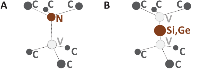
For NV centers, the dominant dephasing process at cryogenic temperatures is caused by charge fluctuations in the solid-state environment. As shown in Fig. 1, the NV center consists of a nitrogen impurity and a neighboring lattice vacancy each occupying a substitutional site. This structure resembles that of a polar molecule and results in electronic orbitals with a large static dipole moment ( Debye). The energy of these electronic orbitals therefore shifts with any applied electric field, resulting in a broadening of the optical transition with charge fluctuations in the environment. The level of charge noise and spectral diffusion can be minimal for NV centers in high-quality single crystal bulk crystals \shortciteBernien2012,sipahigil2012quantum. However, this dephasing process becomes more severe inside nanofabricated structures due to increased exposure to surface and defect states \shortcitefaraon2012coupling.
We recently demonstrated that silicon-vacancy (SiV) \shortciteevans2016narrow,Sipahigil2016 and germanium-vacancy (GeV) \shortcitebhaskar2017 centers in diamond nanophotonic structures maintain their optical coherence with a strong supression of the spectral diffusion observed in NV centers. The origin of this spectral stability for SiV and GeVs can be understood as a consequence of their inversion symmetry \shortcitesipahigil2014indistinguishable. For defects such as SiV and GeV centers (Fig. 1) the impurity atom (Si or Ge) is located at an interstitial site between two lattice vacancies. In this geometry, the impurity atom constitutes an inversion center. Owing to the inversion symmetry of the structure, electronic orbitals are symmetric with respect to the origin and have zero static electric dipole moments. The absence of a static electric dipole moment results in a first-order insensitivity to electric fields for SiVs and GeVs111We note that this property parallels a similar idea based on a charge-insensitive superconducting qubit design (i.e. the transmon qubit) which lead to major advances in circuit quantum electrodynamics in the past decade \shortcitekoch2007.. This allows the incorporation of optical emitters with coherent optical transitions into nanophotonic devices which is the key enabling aspect for the experiments discussed in the following sections.
3 Indistinguishable photons from separated silicon-vacancy centers in diamond
The symmetry properties discussed in Section 2 lead to the absence of spectral diffusion \shortciterogers2014multiple and a narrow inhomogeneous distribution \shortcitesternschulte1994luminescence for SiV centers in bulk diamond. In Ref. \shortcitesipahigil2014indistinguishable, we used SiV centers incorporated in a high-quality single-crystal diamond sample to generate indistinguishable photons from separate emitters. These SiV centers were incorporated in the high-quality crystals during the growth process and displayed a narrow inhomogeneous distribution of GHz. For comparison, the natural linewidth of an SiV center is MHz corresponding to an excited state lifetime of ns. To our knowledge, this ratio of the ensemble inhomogeneous distribution and the natural linewidth is the smallest observed among solid-state quantum emitters \shortciteaharonovich2016solid. This narrow distribution makes SiV centers suitable for indistinguishable photon generation from separated emitters.
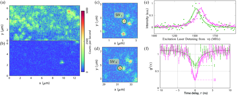
Figs.2(a) and (b) illustrate the narrow inhomogeneous distribution of the SiV centers by showing a comparison of the density of SiV centers at the center frequency () of the inhomogeneous distribution and at a detuning of GHz. When we excite the sample at the center frequency of the ensemble , a high density of emitters are visible with a large backround due to emitters in a different focal plane. Detuning the excitation laser only by GHz from this frequency results in a drastic reduction in the density of visible emitters.
To generate single photons from isolated, single SiV centers and minimize background from other emitters \shortciteMoerner1989, the laser was tuned to the edge of the inhomogeneous distribution ( GHz) where nearly-resonant, single SiV centers can be spatially resolved as shown in Figs. 3(c,d). Photoluminescence excitation (PLE) spectra of the emitters, and , reveal transitions separated by 52.1 MHz with a linewidth of 136 and 135 MHz respectively. For comparison, the lifetime of the excited states was measured to be ns at temperatures below 50 K corresponding to a transform limited linewidth of 94 MHz. The narrow linewidths of the optical transitions are close to the lifetime-limited linewidth, indicating coherent single-photon generation suitable for efficient indistinguishable photon generation.
To test the indistinguishability of the generated photons, single photons from and (Fig. 2 (c,d)) were directed to the input ports 1 and 2 of a beamsplitter respectively. Figure 2 shows two-photon interference \shortciteHong1987 measurements where the degree of indistinguishability of single photons is varied by changing the photon polarization. The two datasets show the second order intensity correlation function, , measured for indistinguishable (II) and distinguishable (I) photon states. For identically polarized indistinguishable photons, we find where the error bars denote shot noise estimates. After rotating the fluorescence polarization of by to make the photon sources distinguishable, was observed. These results clearly demonstrate two-photon interference corresponding to a measured two-photon interference visibility of that is limited by detector timing resolution and background photons \shortcitesipahigil2014indistinguishable.
These observations established the SiV center as an excellent source of indistinguishable single photons with the combination of a strong ZPL transition, narrow inhomogeneous distribution, and spectrally stable optical transitions. These results also suggested the possibility of integrating SiV centers inside nanophotonic cavities to obtain strong coupling \shortciteburek2012free,Hausmann2013,riedrichmoller2012one,lee2012coupling,faraon2012coupling while maintaining their spectral stability. The optical properties of SiV centers in nanophotonic devices will be discussed in Sections 4 and 5.
4 Narrow-linewidth optical emitters in diamond nanostructures via silicon ion implantation
One major advantage of building quantum devices with solid-state emitters rather than trapped atoms or ions is that solid state systems are typically more easily integrated into nanofabricated electrical and optical structures that enable strong light-matter interactions \shortciteladd2010quantum,Vahala2003. The scalability of these systems is important for practical realization of even simple quantum optical devices \shortciteLi2015. Motivated by these considerations and the robustness of the SiV optical transitions in bulk crystals as described in Sec. 3, in Ref. \shortciteevans2016narrow, we studied the optical properties of SiV centers created in diamond nanophotonic structures via Si+ ion implantation.
Silicon-vacancy centers occur only rarely in natural diamond \shortciteLo2014, and are typically introduced during CVD growth via deliberate doping with silane \shortciteEdmonds2008,johansson2011optical or via silicon contamination \shortciterogers2014multiple,neu2013low,clark1995silicon,sternschulte1994luminescence,Zhang2016. While these techniques typically result in a narrow inhomogeneous distribution of SiV fluorescence wavelengths \shortciterogers2014multiple, these samples have a number of disadvantages. For example, the concentration of SiV centers can be difficult to control and localization of SiV centers in three dimensions is not possible. Ion implantation is a commercially available technology that offers a promising solution to these problems. By controlling the energy, quantity, and isotopic purity of the source ions, the depth, concentration, and isotope of the resulting implanted ions can be controlled.
To create SiV centers in bulk diamond, we first implant ions (Innovion Corporation) at a dose of and an energy of 150 keV resulting in the placement of Si atoms at an estimated depth of nm \shortcitesrim. After implantation, we clean the samples using an an oxidative acid clean (boiling 1 : 1 : 1 perchloric : nitric : sulfuric acid) \shortciteHauf2011 and then perform a high-vacuum () anneal at a temperature of C for two hours. At temperatures above C, lattice vacancies can diffuse and combine with the implanted Si ions to form SiV centers. At higher temperatures of C , undesired defect complexes (e.g. divacancies) that can result in magnetic or electric field noise anneal out \shortciteAcosta2009,Yamamoto2013 and partial healing of the lattice damage helps to reduce strain \shortciteOrwa2011.
Following these steps, SiV centers created in bulk diamond via ion implantation were characterized with photo-luminescence excitation (PLE) spectroscopy at K. Based on a comparison of the Si+ ion implantation density and the measured density of SiV centers in the sample, we estimate our SiV creation yield to be 0.5–1%. The PLE measurements in Ref. \shortciteevans2016narrow showed that implanted SiV centers in bulk diamond have narrow optical transitions with linewidths of (mean and standard deviation for N = 13 spatially resolved emitters). Almost all SiV centers had a linewidth within a factor of three of the lifetime limit. For the 13 SiV centers characterized, about half of the optical transitions were in a GHz window.
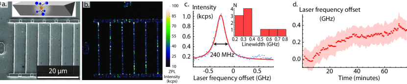
To test the optical coherence of the implanted SiV centers in nanophotonic devices, we fabricated an array of diamond diamond waveguides (Fig. 3a) on the sample characterized above using previously reported methods \shortciteburek2012free,Hausmann2013. Each waveguide (Fig. 3a, inset) is 23 m long with approximately equilateral-triangle cross sections of side length 300–500 nm. After fabrication, we again performed the same annealing and acid cleaning procedure. This process leads to the creation of many SiV centers as seen in the fluorescence image of the final structures of Fig. 3(b).
SiV centers in nanostructures display narrow-linewidth optical transitions with a full-width at half-maximum (FWHM) of (mean and standard deviation for N = 10 emitters; see Fig. 3 inset for linewidth histogram), only a factor of greater than the lifetime limited linewidth . The linewidths measured in nanostructures are comparable to those measured in bulk (unstructured) diamond (). The ratios and are much lower than the values for NV centers, where the current state of the art for typical implanted NV centers in nanostructures\shortcitefaraon2012coupling and in bulk \shortcitechu2014coherent is – and ( for NV centers).
By extracting the center frequency of each individual scan, we also determine the rate of fluctuation of the ZPL frequency and therefore quantify spectral diffusion (Fig. 3d). Optical transition frequencies in SiV centers are stable throughout the course of our experiment, with spectral diffusion on the order of the lifetime-limited linewidth even after more than an hour.
The residual broadening of the optical transition can result from a combination of second-order Stark shifts and phonon-induced broadening. The presence of a strong static electric field would result in an induced dipole that linearly couples to charge fluctuations, accounting for the slow diffusion. Determining the precise mechanisms for the residual broadening of the SiV optical linewidths remains an important topic of future study. It should be possible to test the linear and nonlinear susceptibility of the optical transition frequencies to electric fields by applying large electric fields from nearby electrodes \shortciteAcosta2012. Despite the deviation from an ideal behavior by a factor of in linewidth and in ensemble inhomogenous distribution, the observed optical properties are already sufficient to observe strong atom-photon interactions in photonic crystal cavities with high cooperativity, a topic that will be discussed in the next section.
5 Diamond nanophotonics platform for quantum nonlinear optics
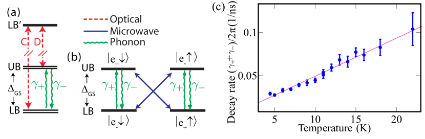
We next review experiments using negatively-charged silicon-vacancy (SiV) color centers coupled to diamond nanophotonic devices that demonstrate strong interactions between single photons and a single SiV center. In Ref. \shortciteSipahigil2016, we created SiV centers inside one-dimensional diamond waveguides and photonic-crystal cavities with small mode volumes () and large quality factors () as illustrated in Fig. 4. These nanophotonic devices are fabricated using angled reactive-ion etching to create free-standing single-mode structures starting from bulk diamond \shortciteburek2012free,burek2014high. A recent review article on different diamond nanophotonic device fabrication approaches can be found in Ref. \shortciteSchroder16.
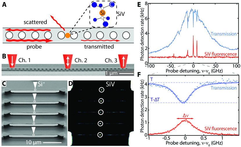
To obtain optimal coupling between the emitter and the cavity mode, the emitter needs to be positioned at the field maximum of the cavity mode. This can be achieved with two possible approaches. In Refs. \shortciteSipahigil2016 and \shortciteSchroder2017, a Si+ ion beam was focused at the center of the cavities to create SiV centers as illustrated in Fig. 4. Using this approach, the emitters can be positioned with close to nm precision which is limited by a combination of ion-beam spot size, alignment errors and straggle in the crystal. An alternative approach is to fabricate lithographically defined small apertures and use commerically available ion beams to implant the Si+ ions \shortciteSchroder16. Using these techniques, a large array of coupled emitter-cavity systems can be fabricated on a single sample.
An example spectrum of the coupled SiV-cavity system at K is shown in Fig. 4. Each narrow dip within the broad cavity transmission band is caused by a single SiV. On SiV resonance, the emitter results in a strong extinction ( ) of cavity transmission \shortciteSipahigil2016. Based on the measurements shown in Fig. 4F, it is possible to infer a cooperativity of for the SiV-cavity system with cavity QED parameters GHz where is the single-photon Rabi frequency, is the cavity intensity decay rate and is the SiV optical transition linewidth, cooperativity is a parameter that characterizes the ratio of coherent coupling rate () with dissipation rates (). We note that the SiV optical transition linewidth of MHz includes the sum of free-space decay, non-radiative decay and pure dephasing rates.
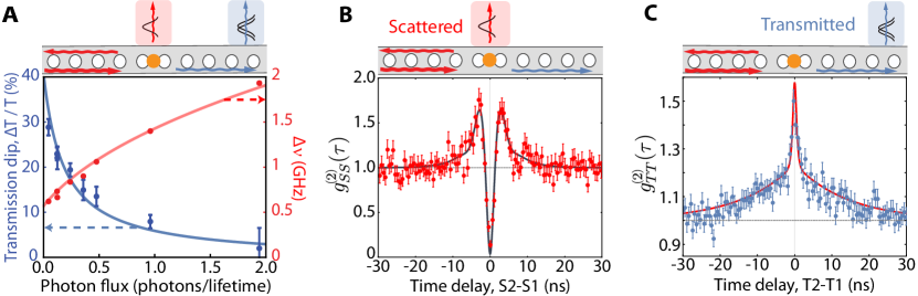
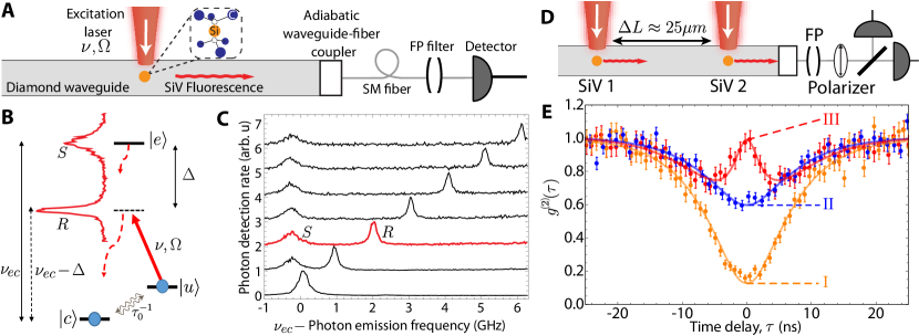
The observed cooperativity of in the experiments marks the onset of nonlinear effects at the single-photon level. Owing to the strong interaction between a single-photon and the SiV center, the SiV is saturated at a flux of single-photon per Purcell enhanced lifetime ( ps) as shown in Fig. 5. In this regime, the strongly coupled SiV-cavity system acts as a photon number sorter that scatters single photons while having a high transmission amplitude for photon pairs due to saturated atomic response. This effect can be observed in photon intensity correlation measurements that show antibunching for the scattered field (Fig. 5(B)) and bunching for the transmitted field (Fig. 5(C)) \shortciteSipahigil2016.
6 Two-SiV entanglement in a nanophotonic device
Experiments discussed in the previous section demonstrated coherent single-photon single-emitter interactions. As seen in Fig. 4 (E), the optical transitions of SiV centers in nanostructures have an inhomogeneous distribution of GHz. This inhomogeneity implies that different emitters will emit spectrally distinguishable photons that are not suitable for photon-mediated interactions between multiple emitters. To generate indistinguishable photons from different nodes, it will be necessary to either improve material properties by reducing the strain variations in the crystal or develop active tuning methods.
To generate spectrally tunable photons, one can use Raman transitions between the metastable orbital states of SiV centers \shortciteSipahigil2016. When a single SiV is excited from the state at a detuning (Fig. 6), the emission spectrum includes a spontaneous component at frequency and a Raman component at frequency that is tunable by choosing . As shown in Fig. 6(C), the Raman emission frequency can be tuned by varying the excitation laser detuning . This technique allows frequency tuning of the Raman emission by GHz which is comparable to the inhomogeneous distribution of SiV centers in nanophotonic devices.
The Raman tuning approach enables the tuning of multiple spatially resolved emitters in a single nanophotonic device into resonance. To achieve this, we applied a separate Raman control field for two SiV centers in the same diamond waveguide (Fig. 6(D)) and measured intensity correalations of Raman photons emitted into the waveguide mode \shortciteSipahigil2016. In this experiment, the two SiVs emit Raman photons into the same spatial mode and the frequency indistinguishability is achieved by Raman tuning. If the Raman emission of the two SiVs are not tuned into resonance, the photons are distinguishable, resulting in the measured (curve II, Fig. 6E) close to the conventional limit associated with two distinguishable single photon emitters . Alternatively, if the Raman transitions of the two SiVs are tuned instead into resonance with each other, an interference feature is observed in photon correlations around zero time delay with (curve III, Fig. 6E).
The observed enhancement of the results from the collectively enhanced decay of the two SiV centers. When the Raman transitions of the two SiVs are tuned into resonance with each other, it is not possible to distinguish which of the two emitters produced a waveguide photon. Thus, the emission of an indistinguishable single photon leaves the two SiVs prepared in the entangled state \shortcitecabrillo1999, where is set by the propagation phase between emitters spaced by and the relative phase of the Raman control lasers. This state is a two-atom superradiant state with respect to the waveguide mode and scatters Raman photons at a collectively enhanced rate that is twice the scattering rate of a single emitter. This enhanced emission rate into the waveguide mode results in the experimentally observed interference peak at short time delays (curve III, Fig. 6E) and is a signature of entanglement.
In these experiments, the coherence time of the entangled state and control over the SiV orbital states is limited by the occupation of GHz phonons at K, which causes relaxation between the metastable orbital states and and limits their coherence times to less than ns. In the following Section, we discuss a microscopic model of this dephasing process and a recent experiment that extended SiV spin coherence to ms by operation at mK.
7 SiV spin coherence at low temperatures
In this section, we focus on the dynamics of the spin and orbital degrees of freedom of the SiV center that are relevant for storing quantum information. In Sec. 1, we first present high temperature ( K) measurements of the electronic orbital relaxation dynamics and a microscopic model of the SiV-phonon interactions that limit spin coherence \shortcitejahnke2015electron. After a discussion of the predictions of this model for low temperatures, we present recent experiments that demonstrate a long coherence time of ms at mK \shortciteSukachev2017 in Sec.2.
1 Electron-phonon processes of the silicon-vacancy center in diamond
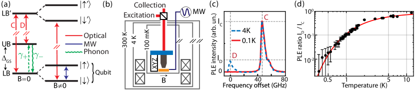
The symmetry properties of the SiV center results in ground () and excited () electronic orbitals that both have symmetry and double orbital degeneracy \shortcitehepp2014electronic. The two degenerate ground state orbitals are occupied by a single hole with resulting in four degenerate ground states with orbital () and spin () degrees of freedom \shortcitejohansson2011optical,rogers2014electronic,hepp2014electronic,Gali2013 . The fourfold degeneracy of the ground states is partially lifted by the spin-orbit interaction ( with GHz) which results in two ground spin-orbit branches (UB, LB in Fig. 7(a)). Each spin orbit branch consists of two degenerate states with well defined orbital and spin angular momentum (in Fig. 7(b)) at zero magnetic field \shortcitehepp2014electronic. Acoustic phonons can also drive spin-conserving transitions between and orbitals, resulting in population transfer between orbitals at rates \shortciteham1965dynamical,fischer1984vibronic.
In Ref. \shortcitejahnke2015electron, the relaxation within the ground state doublet, in Fig. 7 (b), was probed directly using pulsed optical excitation and time-resolved fluorescence measurements. This measurement was repeated for a single SiV center at various temperatures between K and K and the relaxation rate was found to scale linearly with temperature (Fig. 7 (c)). The slowest rate observed was at K. This fast decay mechanism implies that any coherence created between the states shown in Fig. 7 will decay at the ns timescale at K. Recent experiments at K \shortcitepingault2014all,rogers2014all,becker2016ultrafast,pingault2017 that observed coherence times in this range can therefore be explained by this phonon-induced orbital relaxation process.
We next discuss a microscopic model of the orbital relaxation processes within the ground electronic levels. The electron-phonon processes are consequences of the linear Jahn-Teller interaction between the E-symmetric electronic states and E-symmetric acoustic phonon modes \shortcitefischer1984vibronic,maze2011properties,doherty2011negatively. Since the phonons couple to the orbital degree of freedom, phonon transitions are spin-conserving at zero magnetic field and we can focus on the orbital degree of freedom to understand the electronic dynamics of ground levels. For a given spin state, the effective zero-field orbital Hamiltonian takes the following form
| (1) |
where is the usual Pauli operator for orbital states in the basis, is the magnitude the spin-orbit splitting, which is for and for .
The interaction between the orbital states and phonon modes is described most easily if the phonon modes are linearly transformed to be circularly polarized. With this transformation, the phonon Hamiltonian and the linear electron-phonon interaction are
| (2) | ||||
| (3) |
where is the coupling strength for a single phonon, () is the raising (lowering) operator for the orbital states, and () is the creation (annihilation) operator for phonons with polarization and wavevector . The coupling strength and the density of phonon modes are approximately and , respectively, where the overbar denotes the average over all modes with frequency and and are proportionality constants \shortcitefu2009observation,abtew2011dynamic. Treating as a time-dependent perturbation, the first-order transitions between the orbital states involve the absorption or emission of a single phonon whose frequency is resonant with the splitting (see Fig. 7 (b)). The corresponding transition rates are
| (4) |
where is the occupation of the phonon mode with polarization and wavector . Assuming acoustic phonons, performing the thermal average over initial states and the sum over all final states leads to
| (5) |
For temperatures , Eq. (5) can be approximated by a single relaxation rate with a linear temperature dependence
| (6) |
The measurements presented in Fig. 7 demonstrated a linear dependence of decay rates for temperatures below K, but greater than the spin orbit splitting ( K). We therefore conclude that the relaxation mechanisms are dominated by a resonant single phonon process at liquid helium temperatures. For a discussion of higher-order phonon processes that become dominant above K, we refer the reader to Ref. \shortcitejahnke2015electron.
We next discuss the implications of the linear electron-phonon interactions for qubit coherence and approaches that could be used to enhance coherence times. At temperatures above the spin-orbit gap ( K), any coherence formed between the states shown in 7(b) will decohere quickly at the ns timescale limited by . Recent experiments that probed ground state coherences have reported values that are in good agreement with this observation \shortcitepingault2014all,rogers2014all,becker2016ultrafast,pingault2017. Eq. 5 shows that the phonon decay rates that limit coherence are determined by a combination of phonon density of states and occupation () at the energy of the spin-orbit splitting with GHz. Since the interaction with the phonon bath is a Markovian process, dynamical decoupling sequences cannot be applied to extend coherences. To extend , we will therefore focus on approaches that reduce the orbital relaxation rates . The first two approaches focus on reducing phonon occupation to decrease . The occupation depends on the ratio, , of the temperature and the energy splitting between the coupled orbital states. Substantial improvements can be achieved by minimizing this ratio in cooling the sample to lower temperatures ( K). Based on the fit in Fig. 7, the expected orbital relaxation timescale is given by ns which correspond to s at K and ms at K. A recent experiment by \shortciteSukachev2017 operating at these low temperatures will be discussed in Sec. 2. A second approach is to increase by using emitters subject to high strain that increases the splitting between the spin-orbit branches. At the limit of , similar reductions in phonon occupation can be used to suppress relaxation rates at K, an effect that was recently observed in Ref. \shortciteSohn2017. In both cases, only the two lowest energy states constitute a subspace that does not couple to phonons. The lowest two energy states are therefore expected to have long coherence times and could be used as a long-lived spin qubit.
We note that the linear electron-phonon interaction Hamiltonian (Eq. 3) and the resulting single-phonon orbital relaxation process are analogous to the Jaynes-Cummings Hamiltonian and Wigner-Weisskopf model of spontaneous emission used in quantum optics. One can therefore use ideas developed in the context of cavity QED to minimize relaxation rates by use of phononic bandgaps \shortciteBurek16 or strong coupling to well defined nanomechanical modes to realize multi-qubit interactions \shortciteBurek16,Sohn2017.
2 SiV spin at low temperatures: a long-lived quantum memory
Motivated by the prediction of long spin coherence at low temperatures, we probed the coherence properties of single SiV centers at mK temperatures in Ref. \shortciteSukachev2017. The key idea of this experiment can be understood by considering the energy level diagram of the SiV in Fig. 8(a). Application of a magnetic field lifts the degeneracy between the spin-orbit states in the LB ( and abbreviated as and from here onwards) with different spin projections. These states, which are defined as qubit states, decay at a rate determined by the phonon occupation at frequency (Eq. 5). By reducing the occupation of phonon modes at at lower temperatures, one can suppress the rate , leaving the spin qubit in a manifold free from phonon-induced decoherence, thereby increasing spin coherence \shortcitejahnke2015electron.
In Ref. \shortciteSukachev2017, we investigated the SiV spin properties below mK using a dilution refrigerator with a free-space confocal microscope and a vector magnet as shown in Fig. 8(b). We first studied the thermal population of the LB and the UB between and K using an ensemble of as-grown SiV centers to probe the effective sample temperature. We probed the relative populations in the LB and the UB (and therefore the ratio ) by measuring the absorption spectrum of transitions C and D. Transitions C and D were both visible in PLE at 4 K, which indicates comparable thermal population in the LB and UB [Fig. 1(c)]. As the temperature was lowered [Fig.1(d)], the ratio of the transition D and C peak amplitudes () reduces by more than two orders of magnitude and follows \shortcitejahnke2015electron. These measurements demonstrated an orbital polarization in the LB of below mK. At these low temperatures, and the qubit states are effectively decoupled from the phonon bath.
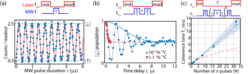
We used microwave fields resonant with the qubit transition to coherently control the SiV spin and probe its coherence \shortciteSukachev2017. In these experiments, single strained SiV centers with GHz are used. When crystal strain is comparable to spin-orbit coupling ( GHz), the orbital components of the qubit states are no longer orthogonal \shortcitehepp2014electronic, leading to an allowed magnetic dipole transition between the qubit states \shortcitepingault2017. Fig. 9 shows measurements where a resonant microwave field drives coherent Rabi oscillations of the spin qubit. In these experiments, a long laser pulse at frequency f first initializes the spin in state via optical pumping. After a microwave pulse of duration , a second laser pulse at f reads out the population in state . Ramsey interference was used to measure the spin dephasing time for SiV centers in two different samples [Fig. 9(b)]. For a sample that contained a low concentration of 13C nuclear spins (Sample-12, blue circles), we measured a dephasing time in the range of s. For a second sample that contained a natural abundance of 13C nuclear spins (Sample-13, red squares), we measured ns which is similar to typical values observed with NV centers. These results demonstrate that the dephasing time of SiV centers is primarily limited by the nuclear spin bath in the diamond host with a natural abundance of 13C \shortciteChildress2006a.
Dephasing due to slowly evolving fluctuations in the environment (e.g. nuclear spins) can be suppressed by using dynamical decoupling techniques \shortciteRyan2010,DeLange2010. We extended the spin coherence time by implementing Carr–Purcell–Meiboom–Gill (CPMG) sequences with , and 32 rephasing pulses \shortciteMeiboom1958 in the isotopically purified sample. Fig. 9(c) shows that the coherence time increases approximately linearly with the number of rephasing pulses . The longest observed coherence time is ms for . Repeating the CPMG sequences for , and 4 with the Sample-13 gave similar coherence times as for Sample-12. Surprisingly, the observation that the coherence time in both samples is identical for a given indicates that the coherence time is not limited by the nuclear spin bath, but by another noise source. While the origin of the noise source is at present not understood, the linear dependence of on suggests that can potentially be further improved by using additional rephasing pulses \shortciteSukachev2017.
These observations establish the SiV center as a promising solid-state quantum emitter for the realization of quantum network nodes using integrated diamond nanophotonics \shortciteSipahigil2016. The demonstrated coherence time of 13 ms is already sufficient to maintain quantum states between quantum repeater nodes separated by km \shortciteChildress2006a. The quantum memory lifetime could be further extended by implementing robust dynamical decoupling schemes \shortciteDeLange2010 or using coherently coupled nuclear spins as longer-lived memories \shortcitemaurer2012room.
8 Outlook
In this Chapter, we reviewed recent progress on the realization of near-deterministic spin-photon interactions based on a single SiV in a cavity and two-emitter entanglement generation in a single nanophotonic device \shortciteSipahigil2016. When combined with the recent demonstration of 13ms spin coherence for SiV centers \shortciteSukachev2017, these advances make SiV centers the first solid-state quantum emitter that has the desired combination of long-lived spin coherence with a deterministic spin-photon interface.
Here we outline several research directions to advance this diamond nanophotonics platform towards the realization of scalable quantum repeater nodes. Our preliminary results with improved cavity designs and emitter positioning yield higher cooperativities of . These advances open up the possibility of realizing deterministic entanglement generation between two-SiVs in a single nanocavity at high rates while maintaining long spin coherence at low temperatures. To achieve this, current experiments are focusing on combining coherent spin control methods \shortciteSukachev2017,Becker2017 and efficient fiber collection from nanophotonic structures \shortciteburek2017 at 100mK. For long-distance quantum communication applications, these devices are expected to improve the entanglement generation rates by many orders of magnitude compared with the state-of-the-art \shortciteRosenfeld2017,hucul2015modular,hensen2015loophole. We expect that these technical improvements will bring the realization of a multi-node quantum repeater within reach. For long-distance quantum communication, the SiV photons should be downconverted to the telecommunication-band for low-loss photon distribution in a fiber network. The improved collection efficiency from the nanophotonic sturctures is expected to result in a high signal-to-noise ratio quantum frequency conversion to the nm telecommunication band with reduced spontaneous noise contribution from a pump in the nm band \shortciteZaske2012.
Finally, other color centers such as the germanium-vacancy (GeV) \shortcitepalyanov2015germanium and the tin-vacancy (SnV) \shortciteiwasaki2017tin centers with similar symmetry properties could yield improved optical and spin properties and recently started being actively explored. The GeV center was demonstrated to be superior to SiV centers in terms of its quantum efficiency \shortcitebhaskar2017 and is expected to show similar spin properties at dilution fridge temperatures \shortciteSiyushev2017. To date, however, there has not been a system that combined good optical and spin properties at higher temperatures of K. In principle, no fundamental reason prevents obtaining spectrally stable optical transitions and long spin coherence times at K. Recent experiments with the neutral silicon-vacancy centers have already started investigating this possibility \shortcitegreen2017,rose2017observation. Considering the existence of hundreds of color centers in diamond \shortciteZaitsev2001, a systematic experimental survey of different color centers with guidance from density functional theory calculations \shortcitegoss2005vacancy is likely to result in new systems with improved device performance at elevated temperatures, which could be instrumental for realizing practical solid-state quantum repeater nodes.
9 Acknowledgements
The work described in this Chapter highlights the results of a collaborative team effort over the past decade. Most of the experiments presented were carried out by members of the Harvard quantum optics group including Ruffin Evans, Denis Sukachev, Mihir Bhaskar, Christian Nguyen and Alexander Zibrov. Furthermore, we are grateful to Fedor Jelezko and members of the Ulm quantum optics group, including Kay Jahnke, Lachlan Rogers, Mathias Metsch and Petr Siyushev for a close collaboration on quantum optics with novel color centers; to Marko Loncar, Hongkun Park and Michael Burek for critical contributions including the development and fabrication of the diamond nanophotonic devices. We additionally acknowledge many discussions and collaborations with Ed Bielejec, Ryan Camacho, and Dirk Englund. This work was supported by the NSF, CUA, AFOSR MURI, ARL CDQI and DURIP Grant No. N00014-15-1-28461234 through ARO.
References
- Abtew et al. (2011) Abtew, T. A., Sun, Y. Y., Shih, B.-C., Dev, P., Zhang, S. B., and Zhang, P. (2011, Sep). Dynamic jahn-teller effect in the center in diamond. Phys. Rev. Lett., 107, 146403.
- Acosta et al. (2009) Acosta, VM, Bauch, E, Ledbetter, MP, Santori, C, Fu, K-MC, Barclay, PE, Beausoleil, RG, Linget, H, Roch, JF, Treussart, F et al. (2009). Diamonds with a high density of nitrogen-vacancy centers for magnetometry applications. Phys. Rev. B, 80(11), 115202.
- Acosta et al. (2012) Acosta, V. M., Santori, C., Faraon, A., Huang, Z., Fu, K.-M. C., Stacey, A., Simpson, D. A., Ganesan, K., Tomljenovic-Hanic, S., Greentree, A. D., Prawer, S., and Beausoleil, R. G. (2012, May). Dynamic stabilization of the optical resonances of single nitrogen-vacancy centers in diamond. Phys. Rev. Lett., 108(20), 206401.
- Aharonovich et al. (2016) Aharonovich, Igor, Englund, Dirk, and Toth, Milos (2016). Solid-state single-photon emitters. Nat. Photon., 10(10), 631–641.
- Albrecht et al. (2013) Albrecht, Roland, Bommer, Alexander, Deutsch, Christian, Reichel, Jakob, and Becher, Christoph (2013). Coupling of a single nitrogen-vacancy center in diamond to a fiber-based microcavity. Phys. Rev. Lett., 110(24), 243602.
- Andrews et al. (2014) Andrews, Reed W, Peterson, Robert W, Purdy, Tom P, Cicak, Katarina, Simmonds, Raymond W, Regal, Cindy A, and Lehnert, Konrad W (2014). Bidirectional and efficient conversion between microwave and optical light. Nat. Phys., 10(4), 321–326.
- Balasubramanian et al. (2009) Balasubramanian, G., Neumann, P., Twitchen, D., Markham, M., Kolesov, R., Mizuochi, N., Isoya, J., Achard, J., Beck, J., Tissler, J., Jacques, V., Hemmer, P. R., Jelezko, F., and Wrachtrup, J. (2009). Ultralong spin coherence time in isotopically engineered diamond. Nat. Mater., 8(5), 383–387.
- Barends et al. (2014) Barends, Rami, Kelly, Julian, Megrant, Anthony, Veitia, Andrzej, Sank, Daniel, Jeffrey, Evan, White, Ted C, Mutus, Josh, Fowler, Austin G, Campbell, Brooks et al. (2014). Superconducting quantum circuits at the surface code threshold for fault tolerance. Nature, 508(7497), 500–503.
- Bechtold et al. (2015) Bechtold, Alexander, Rauch, Dominik, Li, Fuxiang, Simmet, Tobias, Ardelt, Per-Lennart, Regler, Armin, Müller, Kai, Sinitsyn, Nikolai A., and Finley, Jonathan J. (2015). Three-stage decoherence dynamics of an electron spin qubit in an optically active quantum dot. Nat. Phys., 11(12), 1005–1008.
- Becker et al. (2016) Becker, Jonas Nils, Görlitz, Johannes, Arend, Carsten, Markham, Matthew, and Becher, Christoph (2016, nov). Ultrafast all-optical coherent control of single silicon vacancy colour centres in diamond. Nat. Commun., 7, 13512.
- Becker et al. (2017) Becker, Jonas Nils, Pingault, Benjamin, Groß, David, Gündoğan, Mustafa, Kukharchyk, Nadezhda, Markham, Matthew, Edmonds, Andrew, Atatüre, Mete, Bushev, Pavel, and Becher, Christoph (2017). All-optical control of the silicon-vacancy spin in diamond at millikelvin temperatures. arXiv preprint arXiv:1708.08263.
- Bernien et al. (2012) Bernien, H., Childress, L., Robledo, L., Markham, M., Twitchen, D. J., and Hanson, R. (2012, January). Two-Photon Quantum Interference from Separate Nitrogen Vacancy Centers in Diamond. Phys. Rev. Lett., 108(4), 1–5.
- Bernien et al. (2017) Bernien, Hannes, Schwartz, Sylvain, Keesling, Alexander, Levine, Harry, Omran, Ahmed, Pichler, Hannes, Choi, Soonwon, Zibrov, Alexander S., Endres, Manuel, Greiner, Markus, Vuletić, Vladan, and Lukin, Mikhail D. (2017, nov). Probing many-body dynamics on a 51-atom quantum simulator. Nature, 551(7682), 579–584.
- Bhaskar et al. (2017) Bhaskar, M. K., Sukachev, D. D., Sipahigil, A., Evans, R. E., Burek, M. J., Nguyen, C. T., Rogers, L. J., Siyushev, P., Metsch, M. H., Park, H., Jelezko, F., Lončar, M., and Lukin, M. D. (2017, May). Quantum nonlinear optics with a germanium-vacancy color center in a nanoscale diamond waveguide. Phys. Rev. Lett., 118, 223603.
- Briegel et al. (1998) Briegel, H, Dür, W, Cirac, J I, and Zoller, P (1998, dec). Quantum Repeaters : The Role of Imperfect Local Operations in Quantum Communication. Phys. Rev. Lett., 81(26), 5932–5935.
- Burek et al. (2014) Burek, Michael J, Chu, Yiwen, Liddy, Madelaine SZ, Patel, Parth, Rochman, Jake, Meesala, Srujan, Hong, Wooyoung, Quan, Qimin, Lukin, Mikhail D, and Loncar, Marko (2014). High quality-factor optical nanocavities in bulk single-crystal diamond. Nat. Commun., 5, 5718.
- Burek et al. (2016) Burek, Michael J., Cohen, Justin D., Meenehan, Seán M., El-Sawah, Nayera, Chia, Cleaven, Ruelle, Thibaud, Meesala, Srujan, Rochman, Jake, Atikian, Haig A., Markham, Matthew, Twitchen, Daniel J., Lukin, Mikhail D., Painter, Oskar, and Lončar, Marko (2016, Dec). Diamond optomechanical crystals. Optica, 3(12), 1404–1411.
- (18)missing (missing)