Electron-Phonon Coupling Constant of Metallic Overlayers from Specular He-Atom Scattering
Abstract
He atom scattering has been shown to be a sensitive probe of electron-phonon interaction properties at surfaces. Here it is shown that measurements of the thermal attenuation of the specular He atom diffraction peak (the Debye-Waller effect) can determine the electron-phonon coupling constant for ultrathin films of metal overlayers on various close-packed metal substrates. Values of obtained for single and multiple monolayers of alkali metals, and for Pb layers on Cu(111), extrapolated to large thicknesses, agree favorably with known bulk values. This demonstrates that He atom scattering can measure the electron-phonon coupling strength as a function of film thickness on a layer-by-layer basis.
![[Uncaptioned image]](/html/1712.06275/assets/x1.png)
Atom scattering at low energies has a long history as a useful probe of surface properties. Reviews2 ; Reviews ; Farias The most common atomic projectiles are He atoms formed into a monoenergetic beam directed toward the surface with energies in the thermal range, meaning kinetic energies less than 100 meV. From ordered surfaces the scattered spectra consist of sharp diffraction peaks and a background which is composed of both elastically and inelastically reflected particles. In such experiments measurements of elastic diffraction in the scattered spectra give information on surface structure and order. The elastic part of the diffuse intensity scattered continuously over all outgoing angles provides information on disorder such as steps, defects and adsorbates on the surface.Disorder Energy-resolved measurements of the inelastic spectra reveal surface phonon modesDoak as well as localized modes of adsorbates and adsorbate layers.Bertino Among other features that have been measured are the cross sections of adsorbates and defects,CrossSections as well as layer-by-layer crystal growth.Comsa
A unique feature of low energy He atom scattering (HAS) is that the atoms scatter, not from the atomic cores of the target surface, but from the rarefied density of electron states whose wave functions extend outward in front of the outermost layer of surface atoms. Thus, the scattered atoms sense the structure and phonon vibrations of the surface atomic cores only through their contributions to the electron density outside (roughly about 3 Å) above the terminal surface layer. For this reason atom-surface scattering has been demonstrated to be a sensitive probe of the electron-phonon interaction, in metals Skl as well as in semimetals with electron and hole pockets at the Fermi level. 13Tam ; 13Tame ; 13Kra ; Benedek-14 Inelastic He atom scattering has been shown to be proportional to the mode-selected components of the electron-phonon coupling constant . For metal crystal surfaces, inelastic scattering can even detect surface modes for which the largest core displacement amplitudes are located several layers beneath the outermost terminal layer, a property that has been called the quantum sonar effect. Skl The Debye-Waller factor, which describes the thermal attenuation of all quantum scattering features (diffraction, diffuse elastic intensity, and inelastic intensities) has been shown to depend in a straightforward manner on the electron-phonon coupling constant .Manson-JPCL-16 ; Manson-SurfSciRep Recently, Tamtoegl et al. 17Tam have proved with state-of-the-art 3He-spin echo experiments that the method reported in Ref. Manson-JPCL-16 can be extended to the important case of surface quantum-well and Dirac states in topological insulators.
In this Letter we examine experimental studies, using He atoms as probes, of layer-by-layer growth of ordered metallic monolayers on close-packed metal substrates. Such experiments typically monitor the intensity of the specular beam, or a different diffraction peak, under conditions of continuous deposition of the metal of interest, and as each additional layer is completed the intensity reaches a maximum, with intervening minima occurring approximately at half-layer coverage. We demonstrate here that these oscillations in intensity, as well as measurements of the Debye-Waller factor on completed layers, can be used to extract values of associated with individual layer thicknesses. This means that the evaluation of as a function of the thickness of the metallic overlayer can be measured by He atom scattering on a layer-by-layer basis. Such knowledge of the electron-phonon interaction near a surface is important for understanding adsorption, chemisorption and chemical reactions at surfaces, and is certainly important in predicting surface superconductivity.
The Debye-Waller (DW) factor associated with a diffraction peak of intensity is expressed as where is its intensity for a frozen surface, is the DW exponent, is the surface temperature, and and are the final and initial He atom wavevectors. In a harmonically vibrating crystal at sufficiently large temperature is linearly proportional to . At temperatures well below the Debye temperature the DW factor saturates to a value less than one and independent of as a consequence of zero point motion. Thus, is the extrapolation of the intensity in the linear region of back to .
It has recently been shown that the electron-phonon coupling strength (or mass enhancement factor) in the case of conducting surfaces can be obtained from a temperature dependent measure of the DW factor of the specular diffraction peak, in the region where is linear, according to the relation Manson-JPCL-16 ; Manson-SurfSciRep
| (1) |
where is the work function, is the effective electron mass, is the mass of the He atom, is the Boltzmann constant, and is the effective electron density of states (DOS) at the Fermi level referred to the surface unit cell and includes only those states which cause a surface charge density oscillation as a consequence of the thermal vibrational motion of the cores. The energy is the incident energy associated with motion normal to the surface for the given incident angle . In general usage is often corrected by the Beeby correction Beeby in which the normal energy is enhanced by the depth of the attractive adsorption well according to . However, for the alkali metals considered here this has a negligible effect because the well is very shallow, for example the Zaremba and Kohn physisorption theory Zaremba gives for the -Cs surface potential meV, resulting from the sum of the lowest bound state energy meV and the zero-point energy of meV.
Bulk electronic properties of alkali metals can often be approximated as those of a free electron gas, and He atom scattering gives evidence that near the surface the electrons may also be approximated by a free electron gas. The evidence is that He atom scattering from all alkali surfaces thus studied exhibits only a specular diffraction peak and that all other diffraction peaks have negligible intensity. This implies that the electronic density near the surface is very smooth, and justifies the use here of a free electron gas DOS for the region near the surface of alkali metals. Alkali metal crystals have body centered cubic (BCC) structure, and this holds true in the layer-by-layer growth. For all of the alkali metals studied here the layer-by-layer growth builds up also with a BCC structure regardless of the crystal structure or crystalline face orientation of the growth substrate.
An example of the alkali atom experiments is exhibited in Fig. 1 a) which shows, for potassium overlayers on Ni(001), the specular He atom scattering Debye-Waller exponent is a nearly linear function of at small monolayer (ML) numbers Layer9 . Interestingly, the slope increases linearly with ML number for small ML numbers as shown in Fig. 1 b) in terms of the dimensionless quantity defined below in Eq. (2), but eventually the slope saturates for ML numbers greater than . In this case it is for ML number . For thicker films, which for K(110)/Ni(111) were measured up to , the slope remains the same and may be regarded as that of semi-infinite K(110).
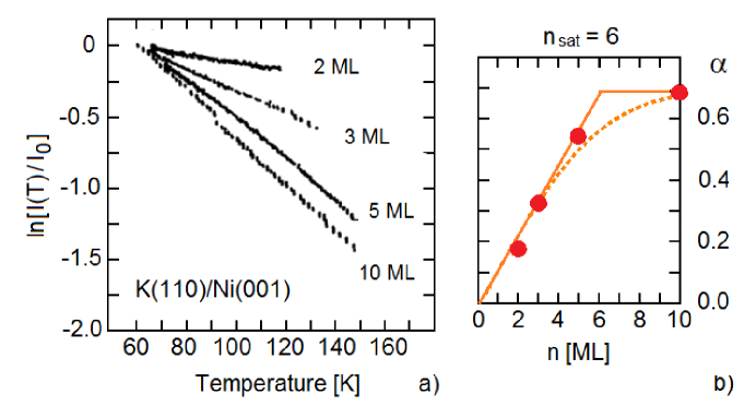
The density of states for a two-dimensional nearly free electron gas is given by . The experimentally observed linear behavior exhibited by successive layers of K in Fig. 1b) at small ML numbers strongly suggests that in this region each monolayer contributes independently to the density of states at the Fermi surface. Theoretical support of this supposition comes from recent calculations of the band structure of free-standing thin films of alkali metals. Bernasconi The DOS can be calculated readily from the band structure. As an example, for a free standing film of up to 11 layers of Cs the band structure shows one parabolic quasi-free electron band per layer, each one contributing the same Fermi level DOS per unit surface area equal to . Bernasconi
This linear increase of the DW slopes shown in Fig. 1b) implies that in Eq. (1) one should use to indicate that in a 2D electron gas representation the layers deeper than do not contribute to the electron-phonon interaction as probed by He atoms at the surface. Then derived from Eq. (1) for any thickness becomes
| (2) |
where the index is used to indicate that the measured specular intensities refer to a film of arbitrary thickness . Here is the area of the surface unit cell and and are any two temperatures in the region where is linear in . Because the dimensionless function , derived from the HAS data and plotted in Fig. 1b), initially grows linearly with n, consequently has about the same value for . The average over the three ( films produces the value . The actual dependence of and can be estimated by considering that the thermal vibrations of deep layers, inducing the surface charge density fluctuations measured by HAS, rapidly decay for increasing . A Gaussian approach of to saturation like with is suggested (broken line in Fig. 1 (b)); at , this yields , consistent with the above average value.
After saturation, i.e., for for the present case of potassium, the slope of the Debye-Waller plot no longer depends on the number of monolayers so it is appropriate to use in Eq. (1) the DOS for a free electron gas, , where is the number of electrons provided by each substrate metal atom and is the Fermi wave vector. Using and 0.27 Å-1 for kF-layer one obtains the same value as found above for , i.e., , which compares favorably with the known tabulated bulk values which range from 0.11 AllenT to 0.130.04 Grimvall .
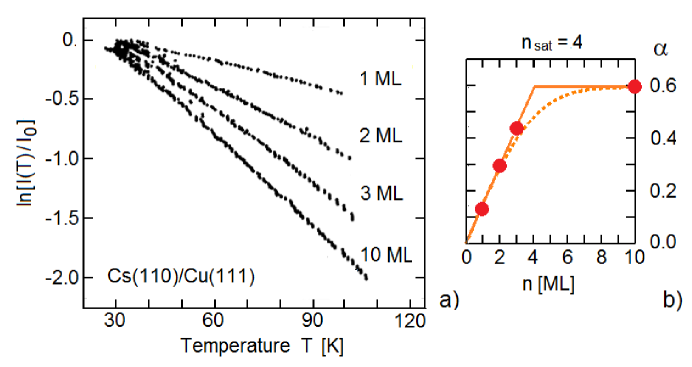
Similar measurements have been made for Cs(110)/Cu(111) as shown in Fig. 2. It is seen that for this system saturation also begins after . In this case the value of produced by the first three layers turns out to be 0.22, if eV is used from Michaelson´s compilation k or 0.18 if we take eV as found in the more recent compilation by Kiejna and Wojciechowski. 81Kie It should be noted that the work function is known to vary in thin films as a function of thickness Qi . Its oscillations are however small as compared to the present level of accuracy, and will be considered only in presence of important quantum size effects, as discussed below for Pb films, while for alkali films the bulk values of are considered a sufficient approximation. At saturation for , again using the three-dimensional free electron DOS in Eq. (1), the value produced is also 0.18 (0.15) which compares favorably with the tabulated bulk values of 0.15 Grimvall and 0.16. AllenT The values of for for these and all the other alkali metal systems studied here, together with more details, are contained in Table 1. The ability to study Cs with He atom scattering is interesting as it is one of the few elements that is difficult to study in the bulk with neutron scattering because of the very high neutron capture cross section of the Cs nucleus. He atom scattering at a Cs surface is not hampered by such problems.
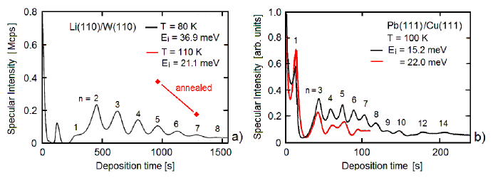
In addition to Debye-Waller plots such as Figs. 1a) and 2a) another important type of measurement which is often carried out is the monitoring of layer-by-layer growth from oscillations in the specular intensity as a function of deposition time, taken at a fixed temperature. An example of Li(110) monolayers deposited on a W(110) substrate at K and meV is shown in Fig. 3. Such measurements provide another method for obtaining the value for by comparing intensities of the oscillation maxima (which occur at full ML coverage) for different ML numbers. Again, this possibility depends on the known linear behavior in temperature of the logarithmic Debye-Waller plots.
To show this consider comparing the intensity maxima for the and monolayers (with both and ) denoted by and , respectively. In general, if layer-by-layer growth plots such as Fig. 3 are carried out at two different temperatures and , with both of these temperatures within the range over which the DW plots are linear in , Eq. (2) can be expanded to produce a value of from the following combination
| (3) |
provided that .
An even simpler expression can be obtained upon recognizing that the extrapolation of the specular intensity to becomes independent of layer number, or can be normalized to the same value as shown in Figs. 1 and 2. Thus, if the intensity at is taken to be that obtained by extrapolation to , Eq. (Electron-Phonon Coupling Constant of Metallic Overlayers from Specular He-Atom Scattering) simplifies to
| (4) |
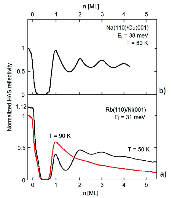
as long as the temperature is within the region for which is linear in . A distinct advantage of using the layer-by-layer growth methods of either Eq. (Electron-Phonon Coupling Constant of Metallic Overlayers from Specular He-Atom Scattering) or (4) is that even if the growth curve is measured at only a single temperature, such as the case for Li(110) in Fig. 3, all combinations of two different peaks provide distinct values of , and this gives sufficient numbers of values for which a standard deviation of error can be evaluated. If the growth plots are carried out at two or more different temperatures, such as the case for Rb(110)/Ni(001) in Fig. 4a), Eq. (Electron-Phonon Coupling Constant of Metallic Overlayers from Specular He-Atom Scattering) can be used and this provides even greater numbers of distinct values for .
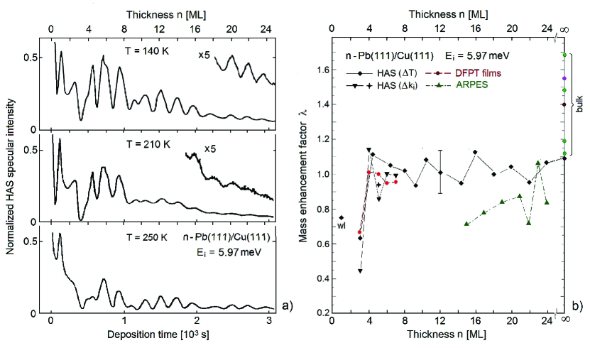
The HAS specular intensity patterns for Li(110) on a W(110) substrate of Fig. 3a) and Na(110)/Cu(001) in Fig. 4 b), both deposited at a temperature of 80 K, show saturation behavior. For Li(110)/W(110) the saturation occurs after and using Eq. (4) the average over gives , while the more restricted average over gives . By comparison the bulk value ranges from AllenT to 0.40 Grimvall . The derivation of from the growth slope could be misleading because the contribution of the e-ph interaction could be obliterated by that because of the accumulation of defects. This is not so however. The available data on the specular intensities of annealed 5 and 7 ML Li(110) films on W(110) (red lozenges in Fig. 3 a)) Layer2 , where defects are nominally absent, yield , in close agreement with the values obtained from the growth slopes. This suggests that the contributions of defects and e-ph interaction to the reduction of the specular intensity with increasing are proportional before saturation, so that the formation of defects has no effect on the intensity ratios of Eqs. (3) and (4). The pattern of Na(110) growth in Fig. 4 suggests a very regular growth, and the average over gives as compared to for bulk Na Grimvall and 0.24 for the surface of a Na quantum well. Layer4 Such a regularity is apparently a property of simple metals. For comparison the layer-by-layer growth of Pb films on Cu(111) (Fig. 3 b)) shows an oscillating decay of the He specular scattering which has been ascribed to the quantum size effect (QSE) l . Nevertheless there is a clear saturation at , which allows to derive from the interval and for meV (Fig. 3 b)) a mass-enhancement factor . There are however some oscillations of when referred to different intervals: e.g., with meV and for it is found while for it is ; on the other hand for meV and one finds (see Table 1). As shown below the QSE causes oscillations of with the film thickness.
With regards to Rb(110)/Ni(001) in Fig. 4a) can be derived from the DW temperature dependence over the range of and for the two different temperatures of 50 and 90 K using both Eqs. (Electron-Phonon Coupling Constant of Metallic Overlayers from Specular He-Atom Scattering) and (4). The average is as compared with the standard bulk value of 0.15. AllenT This bulk value is smaller, and also smaller than the values extracted via Eq. (Electron-Phonon Coupling Constant of Metallic Overlayers from Specular He-Atom Scattering) from the DW plot slopes Layer8 for which are 0.19 at 50 K and 0.22 at 90 K. This suggests that a non-negligible contribution to the decrease of the specular intensity comes from the increase of defects with temperature, as indicated also by the small layer-by-layer oscillations. On the other hand the lack of large oscillations, ostensibly due to defects, does not seem to affect the value of which encompasses the electron-phonon interaction of the whole film as probed by HAS.
It is important to point out another advantage of obtaining from the layer-by-layer growth plots, which is that effects due to disorder and defects tend to cancel. This can be seen from the first line of Eq. (Electron-Phonon Coupling Constant of Metallic Overlayers from Specular He-Atom Scattering); if at and the additional attenuation of the -th and -th peaks due to static disorder is identical, then it cancels. This is evident because the attenuating effect of disorder is usually expressed as a multiplicative factor (sometimes called a characteristic function Beckmann ) applied to each diffraction peak, regardless of whether the disorder is due to small displacements of the surface or due to defects, and in the intensity ratios appearing in Eq. (Electron-Phonon Coupling Constant of Metallic Overlayers from Specular He-Atom Scattering) or (4), such factors cancel. Clearly in the growth spectra such as in Figs. 3 and 4 both disorder and changes in the electron-phonon interaction must play a role in the fact that the layer-by-layer peaks gradually become less pronounced. In some cases the specular intensity reaches a nonzero saturation value, such as for Li(110) in Fig. 3 or Na(110) in Fig. 4b), while in other cases the specular intensity appears to continue decreasing with large coverage such as for Rb at K in Fig. 4. For the systems which exhibit this saturation behavior with coverage it appears reasonable to assume that disorder attenuation is less important and the gradual disappearance of the layer-by-layer peaks is indicative of the influence of the electron-phonon interaction. For the systems that do not exhibit such saturation with coverage the disorder due to defects in the growing overlayer is surely playing a much larger role, but these systems are still amenable to analysis using Eq. (Electron-Phonon Coupling Constant of Metallic Overlayers from Specular He-Atom Scattering) or (4) because, as mentioned above, the effects of disorder tend to cancel out of the ratios of the specular intensity for the same taken at two different temperatures.
The comparatively simple physics concerning the electron-phonon interaction in alkali ultrathin films cannot be straightforwardly extended to other metals such as, for example, lead. The evolution of the HAS specular peak intensity of Pb(111) ultrathin films has been extensively studied as a function of thickness in the layer-by-layer growth regime at different temperatures l ; GZhang ; Braun . Pb films grown on Cu(111) have in common with the alkali films discussed above the fact of being considerably softer than the substrate, which practically restricts the phonon spectrum involved in electron-phonon interaction to that of the film on a rigid substrate Skl . However the HAS normalized specular intensity of Pb films measured during growth as a function of thickness at three different temperatures shown in Fig. 5a) exhibits, over a range up to about 30 Pb layers, rapid oscillations indicating a bilayer-like growth. These growth peaks are further modulated by an envelope of longer-period oscillations, having a length of about 8 layers, which have been convincingly interpreted as quantum size effects l . The comparatively large interlayer distance contraction affecting the topmost bilayer Chulkov ; Yndurain causes the split-off of a surface phonon branch above the bulk phonon spectrum. This explains the bilayer growth mode and suggests that the oscillations of the HAS DW exponent essentially depend on those of the top bilayer 2D electron gas as induced by phonons of the entire film. In this case, an examination of the logarithmic DW plots, similar to Figs. 1 and 2 above, using the three available temperatures of Fig. 5a) indicates that is a reasonable approximation.
The values of derived from Eq. (Electron-Phonon Coupling Constant of Metallic Overlayers from Specular He-Atom Scattering) for the three temperatures of Fig. 5a) are plotted, as a function of the nominal thickness layer number , as filled diamond points connected by solid lines in Fig. 5b). Values of the work function are taken from measurements of as a function of Pb layer thickness on a Si(111) substrate Qi . Meaningful values start from , because the first monolayer of Pb on Cu(111) actually plays the role of a wetting layer, and the second ML film is disordered l ; GZhang . However, the value of extracted from the wetting layer is shown as an isolated diamond marked as “wl”. The vertical bar represents the standard deviation uncertainty. No Beeby correction for the well depth was made in the calculations, but energy dependent measurements of the specular intensity indicate that this is a reasonable approximation as discussed below.
The form of Eq. (1) above makes it clear that can also be obtained from measurements of the DW exponent at fixed temperature, but for two different incident energies. However, such measurements require a correction for the change in intensity of the incident beam as a function of energy. In a series of independent measurements this problem was addressed by changing the source temperature at constant pressure, in which case the supersonic beam flux to a good approximation varies inversely in proportion to . Braun For such a measurement at two different energies the mass enhancement factor is again given by Eq. (2) with the modification that the intensity must be corrected by a factor of and is replaced by
| (5) |
where and are the differences between the respecitve quantities at the two incident energies. Measurements of growth curves of Pb on Cu(111) ) made at K and two incident energies with wavevectors of 5.4 and 6.5 Å-1 (Fig. 3 b)) show bilayer growth of up to for the lower energy and for the larger energy Braun . Plotted in Fig. 5b) as downward-pointing triangles are the values of extracted from this data, and the values are found to be in excellent agreement with those obtained from the temperature dependence at fixed incident energy. It is important to note that the possible dependence on the physisorption well depth through a Beeby correction cancels out in the energy difference of Eq. (5). Thus the good agreement between the energy-dependent and temperature-dependent results shown in Fig. 5b) indicates that the Beeby correction for the well depth is unimportant in these Pb layer systems, and also indicates that the incident beam intensity correction for the energy is a reasonable approximation.
In Fig. 5b) the isolated point at marked with a cross is from the single measurement of the incident energy dependence of the DW exponent taken during the same experiment in which the temperature-dependent data were obtained. GZhang The agreement with the temperature-dependent measurements is quite good.
These extracted values are compared in Fig. 5b) with previous measured values for thick films of 15 to 24 layers using angle-resolved photoemission spectroscopy (ARPES) which lie in the range 0.7 - 1.05 Zhang-05 as shown as upward-pointing triangles connected by dash-dotted lines. Also shown as filled circle points are values for thin films calculated using density functional perturbation theory Skl , and older bulk values in the literature which range from 1.12 to 1.68. Grimvall ; AllenT It is interesting to note that density functional theory calculations for free-standing films (4-10 ML) by Sklyadneva et al. 13Skl yield values of oscillating between 1.1 and 1.3 without spin-orbit interaction, while its inclusion raises to within 1.5 and 2.0, with more prominent quantum-size oscillations. Although the latter results do not agree so well with the present values of , they reveal the relevant contribution to electron-phonon interaction of spin-orbit interaction.
| Growing | (other | ||||||
|---|---|---|---|---|---|---|---|
| layers | sources) | ||||||
| Li(110)/ | 0.261 | 80 | 34.9 | 2.32 Layer1 | 2-5 | 0.47 0.11 | 0.40 Grimvall |
| W(110) Layer2 | 110 | 22.3 | 5-7 | 0.46 0.05 | 0.35 AllenT | ||
| Na(110)/ | 0.119 | 80 | 35.9 | 2.75 k | 2-4 | 0.17 0.03 | 0.16 Grimvall |
| Cu(001) Layer5 | 0.24 Layer4 | ||||||
| K(110)/ | 0.206 | 100 | 27.1 | 2.30 k | 2-6 | 0.16 0.02 | 0.13 Grimvall |
| Ni(001) Layer9 | 0.11 AllenT | ||||||
| Rb(110)/ | 0.296 | 90 | 29.7 | 2.16 k | 2-5 | 0.19 0.06 | 0.16 Grimvall |
| Ni(001) Layer9 | 0.15 AllenT | ||||||
| Cs(110)/ | 0.346 | 75 | 26.9 | 2.14 k | 1-4 | 0.22 0.02 | 0.15 Grimvall |
| Cu(111) Layer9 | 1.81 81Kie | 0.18 0.02 | 0.16 AllenT | ||||
| Pb(111)/ | 1.31 | 100 | 29.2 | 4.1 Qi | 3-9 | 1.18 | 1.12-1.68 Grimvall ; AllenT |
| Cu(111) l | 0.86 | 29.2 | 3-8 | 0.93 | 0.95 Benedek-14 | ||
| 0.97 | 42.3 | 3-7 | 0.90 | 0.7-1.05 Zhang-05 |
It is important to note that in Table I the values of , directly derived from experiment with no specification besides the layer number, the film work function, the surface atom density and the He atom incident momentum, are compared to available bulk values of , either obtained from other experimental methods or theoretically. For alkali films (except Na) turns out to be systematically larger than the bulk by more than 20 . There are different reasons for that worth being elucidated with new HAS experiments and a theoretical refinement. The first possible reason is the intrinsic enhancement of e-ph interaction expected at metals. plummer In supported films may also differ from the surface value for the corresponding semi-infinite crystal due to different electronic structure and lattice dynamics of the substrate. In comparing the measured with bulk values it is implicitily assumed that the substrate is inert, in the sense that its vibrations are sufficiently decoupled from those of the film so as to be unable to modulate the film surface charge density probed by HAS, and its Fermi level electronic states do not contribute appreciably to the surface charge density. This assumption is likely to work well for alkali films, whereas for a few MLs of Pb films on Cu recent embedded atom calculations including the substrate dynamics rusina reveal changes with respect to rigid-substrate calculations, especially for the polarization of the interface phonon which plays a relevant role in quasi-2D superconductivity of Pb ultrathin films Skl ; the fact that in the case of Pb films on Cu the substrate is much smaller than that of the film may compensate the surface enhancement effect.
Finally, the values of derived from the reflectivity of growing films, Eq. (4), may be affected by a positive systematic error due to the increasing number of steps during growth, which yields a faster decrease of reflectivity. However, the reflectivity maxima for increasing measured on annealed samples (an example is shown in Fig. 3a)) turn out to be much larger than but proportional to those for a continuous growth with no annealing, so that no effect is expected on from Eq. (4). In conlcusion, the observed excess of in alkali films with respect to bulk may be considered as a genuine surface enhancement, which may however be corrected by substrate effects as is likely to occur in Pb films on Cu.
In this Letter we have shown that through the use of He atom scattering to monitor the temperature dependence of layer-by-layer growth, the electron-phonon coupling constant can be obtained for systems of metal atomic layers grown on different close packed metal substrates. The method is based on earlier work which showed that the Debye-Waller exponent is directly proportional to for simple metal crystal surfaces, as exhibited in Eq. (1). For the case of the multiple atomic monolayers examined here, namely layers of alkali metals and Pb, it is shown that for small monolayer numbers () the three-dimensional density of electronic states at the Fermi surface which appears in Eq. (1) must be replaced by the two-dimensional density of states contributed by all of the layers. For monolayer thicknesses with the 3D DOS is appropriate. The use of the 2D density of states is supported, at least for alkali metals, by recent calculations of the band structure for free-standing thin films of Cs, where it is found that each successive layer independently contributes a quasi-free parabolic band, implying additivity of the DOS at the Fermi level Bernasconi . This property is empirically confirmed in the data which shows that for both alkali metal and Pb overlayers with the slope of the logarithmic DW versus plots is linearly dependent on the ML number . The values of obtained from the temperature dependence of the DW factors, for both small ML values and for films sufficiently thick to be considered as semi-infinite, compare favorably with known measured bulk values or with previous calculated values.
The fact that the DW exponent is linear in temperature, as shown in Eq. (1), and also linear in ML number for provides a second way of extracting values of . This is through comparing ratios of intensities of a given diffraction peak (usually the specular), measured at full monolayer coverage, but with two different ML numbers and at two different temperatures. Compared to the method of extracting from the slopes of the temperature-dependent Debye-Waller plots, this alternative method has the advantage that attenuation of intensity due to static defects tends to cancel out. It also provides a large number of different ML number combinations, each of which produces a value of , which gives sufficient numbers for providing statistical standard deviations. For the Pb layer-by-layer growth as well as for the alkali metals the alternative method produced values of that were in reasonable agreement with the values obtained from the logarithmic Debye-Waller plots, and which compared favorably with the known bulk values.
The reasonable agreement between the surface values obtained in this work compared to the known bulk values indicates that He atom scattering can measure electron-phonon interaction properties of surfaces, not only for the simple metals for which Eq. (1) was originally derived, but also for more complicated systems such as the metallic layer-by-layer growth systems examined here. In particular, the electron-phonon coupling strength can be measured as a function of the thickness of the film.
Acknowledgment: We would like to thank Profs. M. Bernasconi, E. V. Chulkov and P. M. Echenique (DIPC) for helpful discussions. This work is partially supported by a grant with Ref. FIS2014-52172-C2-1-P from the Ministerio de Economia y Competitividad (Spain).
References
- (1) Goodman, F. O.; Wachman, H. Y. Dynamics of Gas-Surface Scattering; Academic Press: New York; 1976.
- (2) Hulpke (Ed.), E. Helium Atom Scattering from Surfaces; Springer Series in Surface Sciences 27; Springer Press: Heidelberg; 1992.
- (3) Farías, D.; Rieder, K.-H. Atomic Beam Diffraction from Solid Surfaces. Rep. Prog. Phys. 1998, 61, 1575-1664.
- (4) Poelsema, B.; Comsa, G. Scattering of Thermal Energy Atoms from Disordered Surfaces; Springer Tracts in Modern Physics 115; Springer Press: Berlin; 1989.
- (5) Brusdeylins, G.; Doak, R. B.; Toennies, J. P. Observation of Surface Phonons in Inelastic-Scattering of He Atoms from LiF(001) Crystal-Surfaces. Phys. Rev. Lett. 1980, 44, 1417-1420.
- (6) Bertino, M.; Ellis, J.; Hofmann, F.; Toennies, J. P.; Manson, J. R. High-Resolution Helium Scattering Studies of Inelastic Interference Structures of the Frustrated Translational Mode of CO on Cu(001). Phys. Rev. Lett. 1994, 73, 605-608.
- (7) Poelsema, B.; Comsa, G. Scattering of Thermal He from Disordered Surfaces.Faraday Discuss. Chem. Soc. 1985, 80, 247-256.
- (8) Kunkel, R.; Poelsema, B.; Verheij, L. K.; Comsa, G. Reentrant Layer-by-Layer Growth During Molecular-Beam Epitaxy of Metal-on-Metal Substrates. Phys. Rev. Lett. 1990, 66, 733-736.
- (9) Sklyadneva, I. Yu.; Benedek, G.; Chulkov, E. V.; Echenique, P. M.; Heid, R.; Bohnen, K.-P.; Toennies, J. P. Mode-Selected Electron-Phonon Coupling in Superconducting Pb Nanofilms Determined from He Atom Scattering. Phys. Rev. Lett. 2011, 107, 095502.
- (10) Tamtögl, A.; Kraus, P.; Mayrhofer-Reinhartshuber, M.; Campi, D.; Bernasconi, M.; Benedek, G.; Ernst, W. E. Surface and Subsurface Phonons of Bi(111) Measured with Helium Atom Scattering. Phys. Rev. B 2013, 87, 035410.
- (11) Tamtögl, A.; Kraus, P.; Mayrhofer-Reinhartshuber, M.; Campi, D.; Bernasconi, M.; Benedek, G.; Ernst, W. E. Surface and Subsurface Phonons of Bi(111) Measured with Helium Atom Scattering. Phys. Rev. B 2013, 87, 159906 (E).
- (12) Kraus, P.; Tamtögl, A.; Mayrhofer-Reinhartshuber, M.; Benedek, G.; Ernst, W. E. Resonance-Enhanced Inelastic He-Atom Scattering from Subsurface Optical Phonons of Bi(111). Phys. Rev. B 2013, 87, 245433.
- (13) Benedek, G.; Bernasconi, M.; Bohnen, K.-P.; Campi, D.; Chulkov, E. V.; Echenique, P. M.; Heid, R.; Sklyadneva, I. Yu.; Toennies, J. P. Unveiling Mode-Selected Electron-Phonon Interactions in Metal Films by Helium Atom Scattering. Phys. Chem. Chem. Phys. 2014,16, 7159-7172.
- (14) Manson, J. R.; Benedek, G.; Miret-Artés, S. Electron-Phonon Coupling Strength at Metal Surfaces Directly Determined from the Helium Atom Scattering Debye-Waller Factor. J. Phys. Chem. Lett. 2016, 7, 1016-1021.
- (15) Tamtögl, A.; Kraus, P.; Avidor, N.; Bremholm, M.; Hedegaard, E. M. J.; Iversen, B. B.; Bianchi, M.; Hofmann, P.; Ellis, J.; Allison, W.; Benedek, G.; Ernst, W.E. Electron-Phonon Coupling and Surface Debye Temperature of Bi2Te3(111) from Helium Atom Scattering. Phys. Rev. B 2017, 95, 195401.
- (16) Manson, J. R.; Benedek, G.; Miret-Artés, S. Atom Scattering as a Probe of the Surface Electron-Phonon Interaction. Surface Science Reports, unpublished.
- (17) Beeby, J. L. Scattering of Helium Atoms from Surfaces. J. Physics C 1971, 4, L359-L362.
- (18) Zaremba, E.; Kohn, W. Theory of Helium Adsorption on Simple and Noble-Metal Surfaces. Phys. Rev. B 1977, 15, 1769-1781.
- (19) Hulpke, E.; Lower, J.; Reichmuth, A. Strain and Confined Resonances in Ultrathin Alkali-Metal Films. Phys. Rev. B 1996, 53, 13901-13908.
- (20) Campi, D.; Bernasconi, M.; Benedek, G.; Graham, A. P.; Toennies, J. P. Surface Lattice Dynamics and Electron-Phonon Interaction in Cesium Ultra-Thin Films. Phys. Chem. Chem. Phys. 2017, 19, 16358-16364.
- (21) Calculated from .
- (22) Poole, C. P.; Zasadinsky, J. F.; Zasadinsky, R. K.; Allen, P. B. Electron-Phonon Coupling Constants, in Handbook of Superconductivity, Poole, C. P., Jr. ed.; Academic Press: New York, 1999. Ch. 9, Sec. G, pp. 478-483.
- (23) Grimvall, G. The Electron-Phonon Interaction in Metals; North-Holland: New York;1981.
- (24) Michaelson, H. B. Work Function of Elements and its Periodicity. Journal of Applied Physics 1977, 48, 4729-4733.
- (25) Kiejna, A.; Wojciechowski, K. F. Work Function of Metals: Relation between Theory and Experiment. Prog. Surf. Sci. 1981, 11, 293-338.
- (26) Qi, Y.; Ma, X.; Jiang, P.; Ji, S.; Fu, Y.; Jia, J. F.; Xue, Q.-K.; Zhang, S. B. Atomic-Layer-Resolved Local Work Functions of Pb Thin Films and Their Dependence on Quantum Well States. App. Phys. Lett. 2007, 90, 013109.
- (27) Flach, B. Thesis; University of Göttingen: 2000. Besides the data for Li(110)/W(110) reproduced in Fig. 3(a), this thesis reports other unpublished data on HAS drift measurements on 5 and 9 ML Li(110)/W(110) measured at 140 K for varying from 5.2 to 9.2 , from which a value for of is obtained.
- (28) Carlsson, A.; Hellsing, B.; Lindgren, S. A.; Walldén, L. High-Resolution Photoemission from a Tunable Quantum Well: Cu(111)/Na. Phys. Rev. B 1997, 56, 1593-1600. Note: this is a calculated value of for the surface.
- (29) Hinch, B. J.; Koziol, C.; Toennies, J.P.; Zhang, G. Evidence for Quantum Size Effects Observed by Helium Atom Scattering During the Growth of Pb on Cu(111). Europhys. Lett. 1989, 10, 341-346.
- (30) Flach, B.; Hulpke, E.; Sternhögle, X . Characterization of Epitaxial Rubidium Films with Helium-Atom Scattering. Surf. Sci. 1998, 412, 12-23.
- (31) Beckmann, P.; Spizzichino, A. The Scattering of Electromagnetic Waves from Rough Surfaces; The Macmillan Company: New York; 1963, Ch. 5, p. 70.
- (32) Schief, H.; Toennies, J. P. Observation of Valence-Band Structure in the LVV-Auger Spectra of Thin Epitaxial Sodium Layers. Phys. Rev. B. 1994, 50, 8773-8780.
- (33) Braun, J. Thesis; University of Göttingen: 1997. Max-Planck-Institut für Strömungsforschung Report.
- (34) Zhang, G. Thesis; University of Göttingen: 1991. Max-Planck-Institut für Strömungsforschung Report.
- (35) Sklyadneva, I. Yu.; Heid, R.; Bohnen, K.-P.; Echenique, P. M.; Chulkov, E. V. Surface Phonons on Pb(111). J. Phys.: Condens. Matter 2012, 24, 104004.
- (36) Calleja, F.; Vázquez de Parga, A. L.; Anglada, E.; Hinarejos, J. J.; Miranda,R.; Yndurain, F. Crystallographic and Electronic Contribution to the Apparent Step Height in Nanometer-Thin Pb(111) Films Grown on Cu(111). New Journal of Physics 2009, 11, 123003.
- (37) Lang, N. D.; Kohn, W. Theory of Metal Surfaces - Work Function. Phys. Rev. B 1971, 3, 1215-1223, and references therein.
- (38) Zhang, Y. F.; Jia, J.-F.; Han, T.-Z.; Tang, Z.; Shen, Q.-T.; Guo, Y.; Qiu, Z. Q.; Xue, Q.-K. Band Structure and Oscillatory Electron-Phonon Coupling of Pb Thin Films Determined by Atomic-Layer-Resolved Quantum-Well States. Phys. Rev. Lett. 2005, 95, 096802.
- (39) Sklyadneva, I. Yu.; Heid, R.; Bohnen, K.-P.; Echenique, P.M.; Chulkov, E. V. Mass Enhancement Parameter in Free-Standing Ultrathin Pb(111) Films: The Effect of Spin-Orbit Coupling. Phys. Rev. B 2013, 87, 085440.
- (40) Plummer, E. W.; Shi, J.; Tang, S.-J.; Rothenberg, E.; Kevan, S. D. Enhanced Electron–Phonon Coupling at Metal Surfaces. Surf. Sci. Rep. 2003, 74, 251-268
- (41) Rusina, G. G.; Borisova, S. D.; Eremeev, S. V.; Sklyadneva, I. Yu.; Chulkov, E. V.; Benedek, G.; Toennies, J.P. Surface Dynamics of the Wetting Layers and Ultrathin Films on a Dynamic Substrate: (0.5-4) ML Pb/Cu(111). J. Phys. Chem. C 2016, 120, 22304 –22317