Link between the photonic and electronic topological phases in artificial graphene
Abstract
In recent years the study of topological phases of matter has emerged as a very exciting field of research, both in photonics and in electronics. However, up to now the electronic and photonic properties have been regarded as totally independent. Here, we establish a link between the electronic and the photonic topological phases of the same material system and theoretically demonstrate that they are intimately related. We propose a realization of the Haldane model as a patterned 2D electron gas and determine its optical response using the Kubo formula. It is shown that the electronic and photonic phase diagrams of the patterned electron gas are strictly related. In particular, the system has a trivial photonic topology when the inversion symmetry is the prevalent broken symmetry, whereas it has a nontrivial photonic topology for a dominant broken time-reversal symmetry, similar to the electronic case. To confirm these predictions, we numerically demonstrate the emergence of topologically protected unidirectional electromagnetic edge-states at the interface with a trivial photonic material.
I Introduction
The discovery of topological phases of matter was a major breakthrough in modern condensed-matter and electromagnetics research Hasan and Kane (2010); Shen (2012); Lu et al. (2014, 2016); Haldane (2017). The material topology is determined by the global properties of the electronic or photonic bands, which are characterized by some topological invariant, e.g., the Chern number. The topological properties are robust against smooth variations of the system parameters and can only be changed through a phase transition that involves the exchange of topological numbers of different bands by closing and reopening of a band-gap. This characteristic makes the topological properties quite insensitive to fabrication imperfections. Furthermore, perhaps the most remarkable feature of topological materials is their ability to support unidirectional edge states or spin-polarized edge states at the interface with ordinary insulators Halperin (1982); Hatsugai (1993); Kane and Mele (2005); Raghu and Haldane (2008); Silveirinha (2016). This property was demonstrated theoretically and experimentally in a plethora of systems relying on non-reciprocal Camley (1987); Zhukov and Raikh (2000); Haldane and Raghu (2008); Yu et al. (2008); Wang et al. (2009); Ochiai and Onoda (2009); Ao et al. (2009); Poo et al. (2011); Fang et al. (2012); Davoyan and Engheta (2013, 2014); Skirlo et al. (2015); Abbasi et al. (2015); Minkov and Savona (2016); Jin et al. (2016); He et al. (2016); Jin et al. (2017) and reciprocal materials Hafezi et al. (2011); Rechtsman et al. (2013); Khanikaev et al. (2013); Gao et al. (2015); Liu and Li (2015); Chen et al. (2015); Slobozhanyuk et al. (2017); Silveirinha (2017). In particular, topological systems are quite unique platforms for the development of integrated one-way, defect-immune electronic and photonic guiding devices, even though other solutions not based on topological properties may exist Silveirinha (2017).
Topological materials can be divided into two categories depending on whether or not they remain invariant under the time-reversal operation. Historically, the importance of the time-reversal symmetry in the topology of physical systems was underscored by Haldane who demonstrated in his seminal work Haldane (1988) that a broken time-reversal symmetry is the key ingredient to obtain a quantized electronic Hall phase. This important result was some decades later extended to electromagnetism Raghu and Haldane (2008), and since then a variety of strategies to obtain nontrivial photonic topological phases with a broken time-reversal symmetry was proposed Haldane and Raghu (2008); Wang et al. (2009); Ochiai and Onoda (2009); Ao et al. (2009); Poo et al. (2011); Fang et al. (2012); Skirlo et al. (2015); Minkov and Savona (2016); Jin et al. (2016, 2017).
In parallel, recent studies about the reflection of a light beam on 2D materials with a quantized Hall conductivity Kort-Kamp et al. (2015); Cai et al. (2017) have revealed interesting connections between nontrivial electronic and photonic topological properties (namely quantized Imbert-Fedorov, Goos-Hänchen, and photonic spin Hall shifts).
Inspired by these ideas, here we show using the Haldane model Haldane (1988) how a topologically nontrivial electronic material with a quantized Hall conductivity in the static limit can be used as a building block to create a topologically nontrivial photonic material. It is proven that analogous to the electronic counterpart, the photonic band structure is topologically nontrivial when the time-reversal symmetry is the dominant broken symmetry. Thus, our work establishes for the first time a direct link between the electronic and photonic topological properties.
The manuscript is organized as follows. In Sect. II we propose a patterned 2D electron gas (2DEG) with the symmetries of the Haldane model. The structure consists of an array of scattering centers organized in a honeycomb lattice (often referred to as “artificial graphene” Gibertini et al. (2009); Lannebère and Silveirinha (2015)) under the influence of fluctuating static magnetic field with zero mean value. Using a “first-principles” calculation method, we find the values of the Haldane tight-binding parameters and derive the electronic topological phase diagram. In Sect. III, the dynamic conductivity response of the 2D material is calculated with the Kubo formula. The conductivity is used in Sect. III to characterize the photonic properties of the system and derive the natural modes. The photonic Chern numbers are found with an extension of the theory of Silveirinha (2015). It is shown that the transition from a trivial to a nontrivial electronic topological phase in Haldane graphene induces a photonic topological phase transition. Thereby, we unveil the intimate relation between the electronic and photonic topological properties. Furthermore, it is demonstrated with full-wave simulations that the nontrivial photonic topological phase enables the propagation of unidirectional edge states at the interface with an ordinary light “insulator” (i.e., an opaque material with no light states). A brief overview of the main findings of the article is presented in Sect. V.
II Haldane artificial graphene
II.1 Overview of the Haldane model
The Haldane model is a generalization of the tight-binding Hamiltonian of graphene to systems with a broken inversion symmetry (IS) and/or a broken time-reversal symmetry (TRS) Haldane (1988). Analogous to the graphene case, the Haldane Hamiltonian describes a 2D hexagonal lattice with two scattering centers per unit cell. However, in the Haldane model the two sublattices are allowed to be different, and in the model this feature is described by a mass term , which may be positive or negative. When the two sublattices are identical the mass term vanishes and the 2D material is invariant under the inversion operation. Furthermore, the Haldane model takes into account the possible effect of a nontrivial space-varying static magnetic field with a net flux equal to zero. The magnetic field is responsible for breaking the TRS.
The Taylor expansion of the Haldane’s Hamiltonian near and is given by
| (1a) | ||||
| (1b) | ||||
where is the nearest-neighbors distance, is the wavevector taken relatively to or , and are the nearest-neighbors (in different sublattices) and next-nearest-neighbors (in the same sublattice) hopping energies respectively, ’s are the Pauli matrices and
| (2a) | ||||
| (2b) | ||||
are the terms resulting from breaking the IS and/or the TRS at and respectively. These parameters vanish in pristine graphene. The phase factor is determined by the integral of the magnetic vector potential along a path that joins next-nearest-neighbors Haldane (1988).
The Haldane Hamiltonian leads to a two-band model whose upper and lower band eigenfunctions, denoted by and respectively, have energies given by
| (3a) | ||||
| (3b) | ||||
Of course, when the inversion and time-reversal symmetries are preserved , and one recovers the band diagram of pristine graphene with Dirac cones at and . On the other hand, a nonzero () opens an energy gap () at () between the and bands. Remarkably the electronic phases obtained by breaking predominantly the TRS () or the IS () are topologically distinct, leading to different electronic Chern numbers Haldane (1988). The Chern number of the valence band can be written as (see Appendix A):
| (4) |
For convenience, we will refer in the following to the electronic phase with (which has a Chern number and thereby a nonzero Hall conductivity) as the “Hall phase” and to the electronic phase with (which has vanishing Chern number and vanishing static Hall conductivity) as the “insulating phase”.
II.2 Haldane model in a 2DEG
Next, we outline how the Haldane model may be implemented by modifying the “artificial graphene” structure proposed in Gibertini et al. (2009). The main objective is to give some visualization of the system under study and at the same time obtain an estimate for the Haldane’s tight-binding Hamiltonian parameters.
Artificial graphene consists of a 2DEG under the influence of a periodic electrostatic potential with the honeycomb symmetry. As demonstrated in Gibertini et al. (2009); Lannebère and Silveirinha (2015) such system is fully equivalent to graphene in the sense that near the Dirac points the electrons are described by a massless Dirac Hamiltonian with a linear energy dispersion. Therefore, by breaking the TRS and/or the IS it should be possible to emulate the Haldane model in this platform.
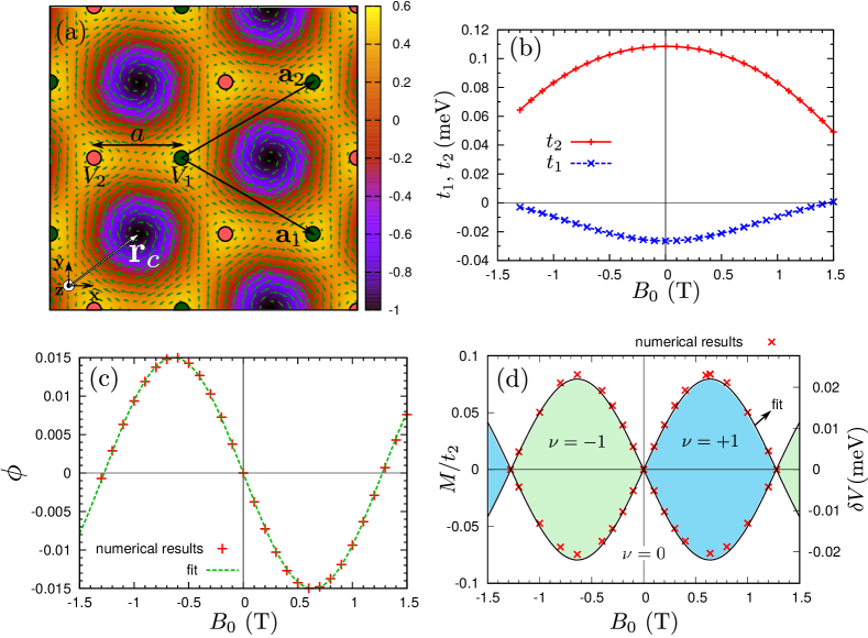
Following Haldane’s idea, a broken IS is implemented by considering different scattering centers for each of the sublattices of the artificial graphene. In our model, the scattering centers are characterized by constant potentials and , and are depicted in Fig. 1(a) as circles with different colors. The region outside the circles has . The broken TRS is achieved with a zero mean-value static magnetic field . The corresponding magnetic potential , defined such that , is supposed to yield a nontrivial flux when the starting and ending points of the integration path are next-nearest neighbors, and a trivial flux when the starting and ending points are nearest neighbors. As illustrated in Fig. 1(a), a magnetic vector potential of the form:
| (5) |
fulfills such requirements. Here is the peak magnetic field amplitude in Tesla, where determines the coordinates of the honeycomb cell’s center (Fig. 1(a)) and the ’s with are the reciprocal lattice primitive vectors. Both and are represented in the honeycomb lattice in Fig. 1(a). Note that the magnetic field is directed along the -direction, perpendicular to the 2D electron gas. Similar to Ref. Lannebère and Silveirinha (2015), it is supposed that the nearest-neighbors distance is and that the radius of the scattering centers satisfies . Even though challenging, in principle the required magnetic field distribution can be created at the nanoscale by nanostructuring permanent magnets.
The tight-binding parameters depend on , and . They are numerically found from “first principles” calculations using the effective medium formalism for electron waves developed in Silveirinha and Engheta (2012) and extended to artificial graphene in Lannebère and Silveirinha (2015) (we use the expression “first principles” in a broad sense with the meaning that the tight-binding parameters are found from a microscopic model). The first step of the method is to solve the Schrödinger equation governing the electron wave propagation in the 2DEG, starting from the “microscopic” Hamiltonian:
| (6) |
where is the electron charge, is the periodic electrostatic potential, is given by (5) and the electron effective mass is as in Ref. Gibertini et al. (2009): , with the electron rest mass. In the spirit of Haldane’s work, the spin interaction is neglected. The Schrödinger equation is numerically solved with the finite differences method Lannebère and Silveirinha (2015). Next, following the homogenization process detailed in Lannebère and Silveirinha (2015), we obtain a effective Hamiltonian that determines the stationary states and the energy dispersion. A detailed analysis (not shown) of the energy diagrams obtained for different values of , and shows that the Haldane model correctly describes the physics of the 2DEG near the Dirac points. Furthermore, the tight-binding parameters can be calculated from a Taylor expansion of the effective Hamiltonian near the Dirac points Lannebère and Silveirinha (2015), which is found to be of the form (1a)-(1b).
The numerically calculated tight-binding parameters are represented in Fig. 1(b)-(c) as a function of the magnetic field intensity for . Note that when the mass parameter vanishes (). Curiously, unlike in graphene, in our system . The hopping constant has a value comparable with that found in Lannebère and Silveirinha (2015). More interestingly, it can be seen that the parameter obtained from the first-principles simulations is a periodic function of and hence is bounded. This feature is not present in the Haldane model wherein is regarded as an arbitrary real-valued number proportional to . The peak value of found here implies that the maximum energy gap, , due to the applied magnetic field is on the order of . The peak is reached for , which may be difficult to create considering that the magnetic field varies at the nanoscale.
To characterize the topology of the 2DEG, we numerically found the combination of parameters and for which the band gap closes at one of the Dirac points, taking and . A nontrivial implies a nonzero tight-binding mass parameter . The calculated phase-diagram is represented in Fig. 1(d) and shows the combination of parameters and for which the band gap closes. Consistent with Haldane (1988), we find that when a band gap closes and reopens there is a topological phase transition and the electronic Chern number changes by one unity. The Chern numbers associated with the energy band are indicated in Fig. 1(d). The electronic Chern number determines the static Hall conductivity in the limit of a zero temperature when the Fermi level is in the band gap Nagaosa et al. (2010); Thouless et al. (1982). The calculated phase-diagram agrees perfectly with Haldane’s theory Haldane (1988), since the periodicity of with induces also a periodicity in the phase-diagram. Thus, similar to Haldane (1988), the broken IS phase corresponds to a trivial electronic Chern number , whereas the broken TRS phase corresponds to a phase with .
As a partial summary, we outlined a physical realization of the abstract notions developed in Haldane (1988), relying on “artificial graphene” and on the periodic magnetic field potential distribution (5). Our study gives the tight-binding parameters obtained from “first-principles” calculations. In the simulations it was assumed that but the design parameters can be renormalized to other values of through a simple dimensional analysis (e.g., a reduction of by a factor of 2 implies an increase of all the involved energies and of by a factor of 4). Even though the practical implementation of the Haldane model in a 2DEG is admittedly very challenging, our study provides for the first time a simple visualization of the concepts introduced in Haldane (1988). In the rest of the article, we use the tight-binding parameters obtained in this section and it is assumed that the relation between and corresponds to the fit of Fig. 1 (c): , with in Tesla.
III Dynamic conductivity of Haldane graphene
In order to characterize the photonic properties of “Haldane graphene”, next we derive its dynamic conductivity with Kubo’s linear response theory Kubo (1966). It is assumed that the valence band is completely filled (the chemical potential is in the gap) and that the temperature satisfies , with the Boltzmann constant and the gap energy. In these conditions, the Hall conductivity in the static limit is determined by the electronic Chern number. Furthermore, the intraband conductivity term vanishes and thereby the dynamic conductivity is given by Mikhailov and Ziegler (2007); Goncalves and Peres (2016); Allen (2006)
| (7) |
where is the Fermi distribution function, is the velocity operator and the sum is over the different bands and . It is implicit that the contributions of both Dirac points are included. Somewhat lengthy but otherwise straightforward calculations based on the continuum version of the Haldane model show that when thermal effects are negligible () the dynamic conductivity is of the form
| (8a) | |||
| where . Thus, in general the material response is gyrotropic, with the anti-diagonal elements of the conductivity tensor given by and the diagonal elements determined by . For real valued with the conductivity elements are given by: | |||
| (8b) | |||
| (8c) | |||
In the above, is a normalized frequency (), and . Remarkably, when the conductivity is independent of the nearest neighbor hopping energy . In the spirit of the Haldane model, it was supposed in the conductivity calculation that the Hamiltonian describes some particular (non-degenerate) electron spin.
A direct inspection of Eq. (8c) reveals that in the absence of a magnetic field (), i.e., when the parameters and are equal, the Hall conductivity is precisely zero. In contrast, for a non-zero magnetic field two distinct situations can occur depending on which broken symmetry is prevalent. Indeed, for relatively low frequencies () the function may be approximated by . In these conditions, the conductivities (8b) and (8c) reduce to
| (9a) | ||||
| (9b) | ||||
| with . | ||||
Equation (9b) confirms that the Hall conductivity in the static limit is quantized and is determined by the electronic Chern number given by (4), which is the TKNN result Thouless et al. (1982); Nagaosa et al. (2010). Thus, consistent with Haldane’s work, we find that the “insulating phase” has a trivial conductivity in the static limit, whereas the “Hall phase” has a quantized Hall conductivity. Furthermore, near the diagonal term is a linear function of the frequency with slope .
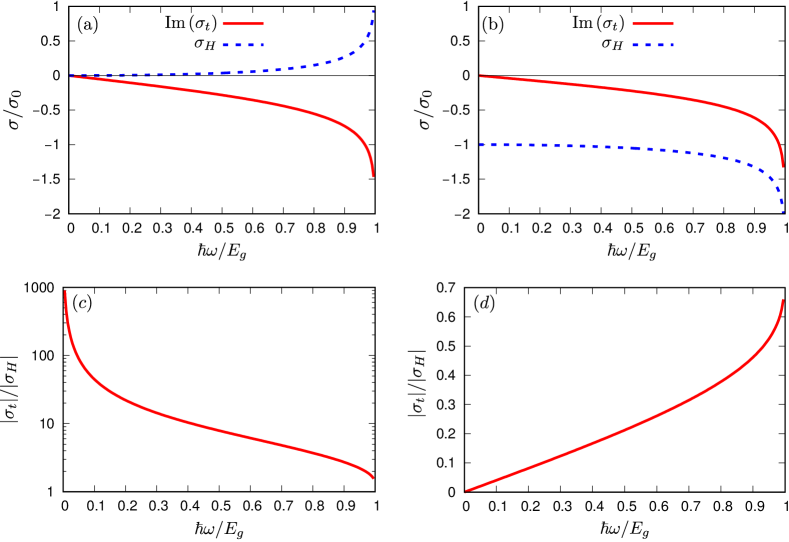
The evolution of the Haldane graphene conductivity as a function of frequency for the “insulating” and “Hall” phases is represented in Fig. 2. In agreement with the phase diagram of Fig. 1 (d) and with Eq. (9b), it is seen that the Hall conductivity at is determined by the Chern number and is nontrivial only in the Hall phase. Perhaps the most striking feature that discriminates the two different phases is the magnitude ratio , represented in Fig. 2(c) and (d). Remarkably, it is much greater than unity for the insulating phase and near zero for the Hall phase. The singularities in the conductivity components near electronic band gap frequency are of logarithmic type.
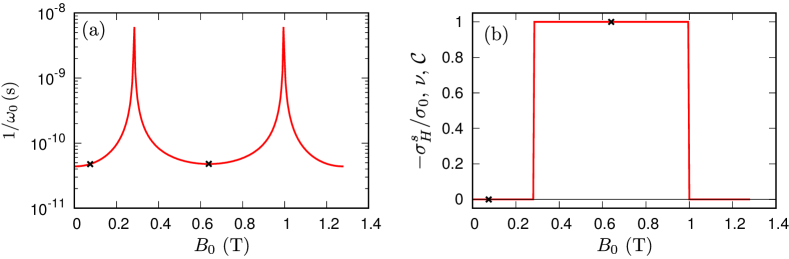
Figure 3 represents the parameter and the static Hall conductivity as a function of the peak magnetic field for a mass parameter . By comparison with the phase diagram of Fig. 1(d), it is seen that the Hall conductivity experiences discontinuous jumps at the topological phase transitions whereas the component remains continuous in the quasi-static limit. It is worth pointing out that the tight-binding parameters used in Fig. 2 (which will be adopted in the rest of the article) yield values for that are comparable for both phases.
To conclude, it is highlighted that Haldane graphene in the Hall phase has a quasi-static conductivity response analogous to that of a magnetized plasma. Indeed, in the limit a lossless magnetized plasma is also characterized by a purely imaginary that vanishes in the static limit and by a nonzero (but not quantized) Bittencourt (2010). However, the two systems are generically rather different. While a decrease of the magnetic field amplitude transforms Haldane graphene into an insulating material (), the conductivity of an electron gas is always nontrivial even when is set identical to zero because the free-electron concentration is finite. Thus, the physical platform discussed in this article has quite unique properties, and generically behaves differently from a 2D magnetized plasma, particularly when the time reversal symmetry is preserved.
IV Photonic topological properties
Next, we characterize the photonic topological properties of the Haldane graphene. In particular, we study the low-frequency photonic phase transition induced by an electronic transition between the insulating and Hall phases, and highlight the relation between the nontrivial electronic and photonic topologies.
The rigorous definition of Chern numbers is only possible for an electromagnetically closed system, and thereby an isolated Haldane graphene sheet does not provide a suitable platform to observe a photonic topological phase transition. Thus, we consider a periodic arrangement of Haldane graphene sheets separated by a distance and embedded in a dielectric of permittivity , as shown in Fig. 4.
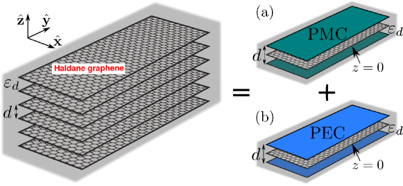
We are interested in waves for which the electromagnetic energy is allowed to flow only in the -plane. Due to symmetry reasons the electromagnetic modes (periodic in ) of the periodic system can be split into two subsets depending on the parity of the fields with respect to the plane : the modes of a waveguide with perfect magnetic conducting (PMC) walls (with even and odd) and the modes of a waveguide with perfect electric conducting (PEC) walls (with odd and even) as illustrated in Fig. 4. Note that the designations even and odd are used here with respect to a reference system with origin in the plane .
Importantly, it can be shown that for a waveguide with PEC walls (system of Fig. 4(b)) all the modes that interact with the Haldane graphene are cut-off at low frequencies. This means that to study the low frequency modes of the periodic arrangement of Haldane graphene sheets it is enough to consider the system of Fig. 4(a), being implicit that the excitation should respect the indicated parity-symmetry of the fields. For this reason in the rest of this paper we will restrict our attention to the system with PMC walls of Fig. 4(a).
IV.1 Natural modes
Next, we derive the natural (guided) modes supported by the structure of Fig. 4(a). Because the system is invariant to translations along the and directions, the guided waves depend on the and coordinates as with the (transverse) wavevector. Furthermore, in the dielectric regions the guided modes are superposition of plane waves. The modes may be split into modes with even and modes with odd (here, the designations even and odd are with respect to the plane). The modes with odd do not interact with the Haldane graphene sheet, and hence are not interesting to us. They have a dispersion of the form , with , and hence are cut-off for low-frequencies.
As to the modes with even, a straightforward analysis shows that the electromagnetic field distribution that satisfies the PMC boundary conditions () and ensures the continuity of the tangential electric field at the graphene-dielectric interface is of the form:
| (10a) | ||||
| (10b) | ||||
where , , and , are (unknown) complex-valued coefficients. Using the boundary condition for the tangential component of the magnetic field at the graphene-dielectric interface, , one obtains the following homogeneous system of equations
| (11) |
whose solutions give the natural modes of oscillation of the system. The dispersion equation is obtained by setting the determinant of the matrix identical to zero
| (12) |
The solutions of the above equation determine the photonic band diagram. It is interesting to note that the limit yields the standard dispersion equation of magnetoplasmons Chiu and Quinn (1974); Ferreira et al. (2012); Goncalves and Peres (2016) (with no PMC walls). Furthermore, a similar analysis shows that the dispersion of a waveguide with PEC walls is given by a similar expression with “” in the place of “”.
The electromagnetic modes , associated with a given are obtained from Eqs. (10a) and (10b) with the coefficients and given by (see Eq. (11))
| (13a) | ||||
| (13b) | ||||
and .
It is useful to consider the solutions of the dispersion equation (12) for a conductivity model with and a constant (frequency independent) . For this model reduces to the static conductivity of Haldane graphene in the “Hall phase”. As shown below, it provides a good approximation of the optical response of Haldane graphene at low frequencies. The modal dispersion with this model is
| (14) |
with . The modes with are evidently cut-off for low frequencies, and hence in the following we focus on the mode with . In the limit this mode follows the light line, and is clearly a transverse electromagnetic (TEM) wave with magnetic field along and electric field parallel to the plates. For a finite , the mode interacts with the Haldane graphene sheet and this opens a band gap in the dispersion diagram, with a cut-off frequency . The cut-off frequency is inversely proportional to the distance between the waveguide walls and approaches zero when . The attenuation factor in the direction normal to the graphene plane is , and hence it is pure imaginary for implying that the natural mode is not guided by the 2D material but rather by the waveguide walls.
In the case of a quantized Hall conductivity , the cut-off frequency can be expressed in terms of the fine structure constant : and the associated wavelength (in host dielectric) at the gap edge is well approximated by . Thus, for this small value of the distance is ultra-subwavelength at the cut-off frequency.
IV.2 Band diagrams and photonic Chern numbers
Figure 5 shows the low-frequency photonic band diagram for the different electronic topological phases of Haldane graphene and two values of the distance . In this calculation, we used the conductivity responses of Fig. 2. Note that the photonic band diagram shows both positive and the negative frequency solutions.
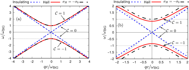
Consistent with the discussion in Sect. IV.1, the band diagrams reveal (for both values of ) that the dispersions induced by the distinct electronic phases are different: in the insulating phase the dispersions follow closely the light line, whereas in the Hall phase the diagram has a low-frequency band gap. The modes in the insulating phase lie outside the light cone and hence are guided by the graphene sheet. In contrast, in the Hall phase the dispersion lies inside the light cone and the wave is – as predicted by the static conductivity model– guided by the waveguide walls. Furthermore, as seen in Fig. 2 the static conductivity model with and gives overall a fairly good approximation of the modal dispersion. The approximation is better for larger values of , when with the interband absorption threshold.
From the eigenmodes expression (10a) and (10b) it is possible to compute the Chern number for each photonic band. The calculation details are given in Appendix B. The approach is based on an extension to layered structures of the theory of Silveirinha (2015, 2016).
The values of the photonic Chern number for each branch are depicted as insets in Fig. 5. The photonic Chern numbers of the bands associated with the electronic insulating phase are equal to zero, whereas they are nontrivial, with values , for the bands associated with the Hall phase. Thus, the electronic topological transition from the insulating to the Hall phase (see Fig. 3), induces the band-gap opening at accompanied by the exchange of photonic Chern numbers between the positive and negative frequency bands, and thereby a photonic topological phase transition. As expected Avron et al. (1983), the total Chern number for each phase is conserved throughout this transition. Remarkably, the topological photonic properties of the material are directly linked to its electronic counterparts such that the electronic Chern number of the valence band is equal to the photonic Chern number of the positive frequency branch: , as shown in Fig. 3(b). This result proves that a biasing magnetic field with a vanishing flux enables a nontrivial photonic topology, similar to the Haldane result for the electronic case.
IV.3 Unidirectional edge-states
According to the bulk-edge correspondence Silveirinha (2016), one may expect that an interface of the Hall phase of Haldane graphene and a trivial photonic insulator may support topologically protected edge-states that span the entire common band-gap. The existence of such unidirectional topologically protected edge-states is demonstrated next with full wave simulations. The trivial photonic insulator is implemented with the same waveguide but with a PEC plate in the place of the Haldane graphene. It may be checked that the modes supported by such a structure are cut-off in the long wavelength limit.
We used CST Microwave Studio CST to demonstrate the emergence of the topological edge states. The optical response of a 2D material sheet with 2D conductivity can be emulated with an equivalent 3D material with thickness and an equivalent permittivity . The thickness must be much smaller than the wavelengths of interest and in addition , and was taken equal to in the numerical study.
In the simulations, the response of the Haldane graphene conductivity in the Hall phase is as shown in Fig. 2(b). The waveguide height is . The structure is excited with a small dipole antenna (polarized along the -direction) located in the close proximity of the interface of the two waveguide regions, with the oscillation frequency in the band-gap ().
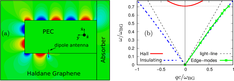
A time snapshot of the component of the magnetic field is represented in Fig. 6(a) for the frequency . As seen, a unidirectional edge state propagating along the direction is excited in the bottom region at the interface between the PEC material and Haldane graphene. A time animation of the magnetic field is available in the supplementary online materials Supplemental Material with the time animation of Fig. 6a, showing the propagation of the unidirectional edge state along the interface and further highlights that this edge state propagates along the interface, regardless of the sharp corners, before reaching an absorber on the right side region. By fitting the wavelength of the guided modes we numerically determined the dispersion of the edge-states as presented in Fig. 6(b). As seen, the edge-modes exist in the entire band gap and closely follow the dispersion of the insulating photonic phase of the Haldane graphene. The low frequency part of the curve was obtained by interpolation because the guided wavelength approaches infinity.
In the waveguide environment, the edge-state is topologically protected against the scattering by an arbitrary three-dimensional defect, and in particular it is protected against sideway scattering Gangaraj et al. (2016). The same property holds (for the relevant wave polarization, i.e., for quasi-transverse magnetic waves) in a periodic array of Haldane graphene sheets, but in this case only for two-dimensional defects uniform along the -direction. Indeed, for a periodic material there are additional radiation channels, for example, the modes that propagate off-plane or the TEM wave with electric field normal to the graphene plane. Note that this constraint on the defects geometry and wave polarization also applies to conventional designs based on gyrotropic media Gangaraj et al. (2016).
Even though in the numerical simulations the response of the Haldane graphene was assumed lossless (consistent with the theoretical model), we checked that the presence of moderate loss does not affect significantly the edge state propagation in the simulation (not shown).
V Conclusions
The work developed in this article is divided into two parts. In the first part we verified using a “first-principles” mean field theory the validity of the Haldane model for a honeycomb lattice with broken TRS and IS. We proposed a magnetic field distribution that mimics the main features of Haldane’s theory, and found the dependence of the tight binding parameters on the magnetic field in artificial graphene. The electronic phase diagram showing the range of parameters for which the magnetized artificial graphene is topologically nontrivial and the quantized Hall conductivity is nonzero was determined.
In the second part, we investigated the optical response of the 2D topological material. The dynamic electric conductivity of Haldane graphene was found with the Kubo formula for a filled valence band. Using this result, we determined the guided modes and the (low-frequency) photonic band diagram of a periodic stack of Haldane graphene sheets. As a fingerprint of the quantized conductivity, the cut-off frequency of the low-frequency band-gap is written in terms of the fine structure constant.
Furthermore, our analysis reveals that the electronic phase transition between the insulating and Hall phases induces a photonic phase transition through the opening of a band-gap at and an exchange of Chern numbers between the positive and negative frequency bands. Interestingly, the electronic and photonic topological properties of this system are intimately related, and we find that the electronic and photonic Chern numbers are identical. In particular, our results imply that a biasing magnetic field with zero net flux can induce a nontrivial topological photonic response. Finally, in agreement with the bulk-edge correspondence, it was shown that the nontrivial photonic phase of Haldane graphene supports topologically protected unidirectional edge states at the interface with an ordinary photonic insulator.
Appendix A The electronic Chern number
In the framework of the exact Haldane Hamiltonian, the electronic Chern number of the -th band is given by
| (15) |
where is the Berry potential and the integration is over the entire Brillouin zone. The Berry potential is written in terms of the energy eigenfunctions. A suitable globally defined gauge of eigenfunctions for the valence band is
| (18) |
In the above, with represent the elements of the exact Haldane Hamiltonian and is the exact energy dispersion of the valence band (see Eq. (1) of Ref. Haldane (1988)). The Berry potential of the valence band is given by:
| (19) |
It is evidently a smooth function of the wave vector, except possibly at the points wherein the considered gauge vanishes, i.e., at the points of the Brillouin zone for which and . A straightforward analysis using the analytical formula of Haldane (1988), reveals that the only possible singularities are the high-symmetry points and . Hence, using Stokes theorem it is possible to reduce the calculation of the valence band Chern number to two contour integrals surrounding the points and :
| (20) |
Here, stands for a circumference (with anti-clockwise orientation) of arbitrarily small radius centered at the point . Explicit calculations show that:
| (21) |
with and . Substitution of this result into Eq. (20) yields the electronic Chern number (4).
Appendix B The photonic Chern number
In this appendix, we present the derivation of the Berry potential and photonic Chern number for the system of Fig. 4. The derivation is an extension of the theory developed in Silveirinha (2015, to appear; available online in arxiv.org/abs/1712.04272) to the case of -stratified inhomogeneous closed systems. For the sake of brevity, we reuse here the notations and concepts introduced in Silveirinha (2015). For more information the reader is referred to Silveirinha (2015).
The electromagnetic modes of the system satisfy the homogeneous Maxwell’s equations
| (22) |
where is a six-vector whose components are the electric and the magnetic fields. In the above, is a differential operator
| (23) |
and is the material matrix. For the system of Fig. 4 with a conductivity sheet centered at , the material matrix is of the form
| (24) |
where is the 2D conductivity and is the material matrix of the surrounding dielectric.
The electromagnetic fields are Bloch waves, , where the field envelope depends only on the coordinate and . The Berry potential is defined from the Hermitian formulation of the Maxwell equations, and can be written as
| (25) |
where the ’s are generalized state vectors (see Silveirinha (2015)), denotes a weighted inner product and . In the case of a -stratified inhomogeneous system, the weighted inner product may be defined such that
| (26) |
Furthermore, it can be shown that the numerator of Eq. (25) satisfies:
| (27) |
The previous results generalize Eqs. (10) and (14) of Silveirinha (2015) to the case of -stratified closed systems. In particular, for the geometry of Fig. 4, the Berry potential (25) is given by
| (28) |
where is the part of the electric field tangential to the conductivity sheet and .
As explained in Silveirinha (2015), for systems invariant under rotations along the -axis the Chern number of a given band is simply
| (29) |
where and is the azimuthal unit vector in a system of polar coordinates. Even though the 2D wave vector space is unbounded, for a nondispersive dielectric host and for the model (9) the Chern number is necessarily an integer because for any band one has in the limit, and the response becomes reciprocal when Silveirinha (2015).
References
- Hasan and Kane (2010) M. Z. Hasan and C. L. Kane, “Colloquium : Topological insulators,” Rev. Mod. Phys. 82, 3045–3067 (2010).
- Shen (2012) S.-Q. Shen, Topological Insulators, Springer Series in Solid-State Sciences, Vol. 174 (Springer, Berlin, Heidelberg, 2012).
- Lu et al. (2014) L. Lu, J. D. Joannopoulos, and M. Soljačić, “Topological photonics,” Nat. Photonics 8, 821–829 (2014).
- Lu et al. (2016) L. Lu, J. D. Joannopoulos, and M. Soljačić, “Topological states in photonic systems,” Nat. Phys. 12, 626–629 (2016).
- Haldane (2017) F. D. M. Haldane, “Nobel lecture: Topological quantum matter,” Rev. Mod. Phys. 89, 040502 (2017).
- Halperin (1982) B. I. Halperin, “Quantized Hall conductance, current-carrying edge states, and the existence of extended states in a two-dimensional disordered potential,” Phys. Rev. B 25, 2185–2190 (1982).
- Hatsugai (1993) Y. Hatsugai, “Chern number and edge states in the integer quantum Hall effect,” Phys. Rev. Lett. 71, 3697–3700 (1993).
- Kane and Mele (2005) C. L. Kane and E. J. Mele, “ Topological Order and the Quantum Spin Hall Effect,” Phys. Rev. Lett. 95, 146802 (2005).
- Raghu and Haldane (2008) S. Raghu and F. D. M. Haldane, “Analogs of quantum-Hall-effect edge states in photonic crystals,” Phys. Rev. A 78, 033834 (2008).
- Silveirinha (2016) M. G. Silveirinha, “Bulk-edge correspondence for topological photonic continua,” Phys. Rev. B 94, 205105 (2016).
- Camley (1987) R. E. Camley, “Nonreciprocal surface waves,” Surf. Sci. Rep. 7, 103–187 (1987).
- Zhukov and Raikh (2000) L. E. Zhukov and M. E. Raikh, “Chiral electromagnetic waves at the boundary of optical isomers: Quantum Cotton-Mouton effect,” Phys. Rev. B 61, 12842–12847 (2000).
- Haldane and Raghu (2008) F. D. M. Haldane and S. Raghu, “Possible Realization of Directional Optical Waveguides in Photonic Crystals with Broken Time-Reversal Symmetry,” Phys. Rev. Lett. 100, 013904 (2008).
- Yu et al. (2008) Z. Yu, G. Veronis, Z. Wang, and S. Fan, “One-Way Electromagnetic Waveguide Formed at the Interface between a Plasmonic Metal under a Static Magnetic Field and a Photonic Crystal,” Phys. Rev. Lett. 100, 023902 (2008).
- Wang et al. (2009) Z. Wang, Y. Chong, J. D. Joannopoulos, and M. Soljačić, “Observation of unidirectional backscattering-immune topological electromagnetic states,” Nature 461, 772–775 (2009).
- Ochiai and Onoda (2009) T. Ochiai and M. Onoda, “Photonic analog of graphene model and its extension: Dirac cone, symmetry, and edge states,” Phys. Rev. B 80, 155103 (2009).
- Ao et al. (2009) X. Ao, Z. Lin, and C. T. Chan, “One-way edge mode in a magneto-optical honeycomb photonic crystal,” Phys. Rev. B 80, 033105 (2009).
- Poo et al. (2011) Y. Poo, R.-X. Wu, Z. Lin, Y. Yang, and C. T. Chan, “Experimental Realization of Self-Guiding Unidirectional Electromagnetic Edge States,” Phys. Rev. Lett. 106, 093903 (2011).
- Fang et al. (2012) K. Fang, Z. Yu, and S. Fan, “Realizing effective magnetic field for photons by controlling the phase of dynamic modulation,” Nat. Photonics 6, 782–787 (2012).
- Davoyan and Engheta (2013) A. R. Davoyan and N. Engheta, “Theory of Wave Propagation in Magnetized Near-Zero-Epsilon Metamaterials: Evidence for One-Way Photonic States and Magnetically Switched Transparency and Opacity,” Phys. Rev. Lett. 111, 257401 (2013).
- Davoyan and Engheta (2014) A. Davoyan and N. Engheta, “Electrically controlled one-way photon flow in plasmonic nanostructures,” Nat. Commun. 5, 5250 (2014).
- Skirlo et al. (2015) S. A. Skirlo, L. Lu, Y. Igarashi, Q. Yan, J. Joannopoulos, and M. Soljačić, “Experimental Observation of Large Chern Numbers in Photonic Crystals,” Phys. Rev. Lett. 115, 253901 (2015).
- Abbasi et al. (2015) F. Abbasi, A. R. Davoyan, and N. Engheta, “One-way surface states due to nonreciprocal light-line crossing,” New J. Phys. 17, 063014 (2015).
- Minkov and Savona (2016) M. Minkov and V. Savona, “Haldane quantum Hall effect for light in a dynamically modulated array of resonators,” Optica 3, 200–206 (2016).
- Jin et al. (2016) D. Jin, L. Lu, Z. Wang, C. Fang, J. D. Joannopoulos, M. Soljačić, L. Fu, and N. X. Fang, “Topological magnetoplasmon,” Nat. Commun. 7, 13486 (2016).
- He et al. (2016) C. He, X.-C. Sun, X.-P. Liu, M.-H. Lu, Y. Chen, L. Feng, and Y.-F. Chen, “Photonic topological insulator with broken time-reversal symmetry,” Proceedings of the National Academy of Sciences 113, 4924–4928 (2016).
- Jin et al. (2017) D. Jin, T. Christensen, M. Soljačić, N. X. Fang, L. Lu, and X. Zhang, “Infrared Topological Plasmons in Graphene,” Phys. Rev. Lett. 118, 245301 (2017).
- Hafezi et al. (2011) M. Hafezi, E. A. Demler, M. D. Lukin, and J. M. Taylor, “Robust optical delay lines with topological protection,” Nat. Phys. 7, 907–912 (2011).
- Rechtsman et al. (2013) M. C. Rechtsman, J. M. Zeuner, Y. Plotnik, Y. Lumer, D. Podolsky, F. Dreisow, S. Nolte, M. Segev, and A. Szameit, “Photonic Floquet topological insulators,” Nature 496, 196–200 (2013).
- Khanikaev et al. (2013) A. B. Khanikaev, S. H. Mousavi, W.-K. Tse, M. Kargarian, A. H. MacDonald, and G. Shvets, “Photonic topological insulators,” Nat. Mat. 12, 233–239 (2013).
- Gao et al. (2015) W. Gao, M. Lawrence, B. Yang, F. Liu, F. Fang, B. Béri, J. Li, and S. Zhang, “Topological Photonic Phase in Chiral Hyperbolic Metamaterials,” Phys. Rev. Lett. 114, 037402 (2015).
- Liu and Li (2015) F. Liu and J. Li, “Gauge Field Optics with Anisotropic Media,” Phys. Rev. Lett. 114, 103902 (2015).
- Chen et al. (2015) W.-J. Chen, Z.-Q. Zhang, J.-W. Dong, and C. T. Chan, “Symmetry-protected transport in a pseudospin-polarized waveguide,” Nat. Commun. 6, 8183 (2015).
- Slobozhanyuk et al. (2017) A. Slobozhanyuk, S. H. Mousavi, X. Ni, D. Smirnova, Y. S. Kivshar, and A. B. Khanikaev, “Three-dimensional all-dielectric photonic topological insulator,” Nat. Photonics 11, 130–136 (2017).
- Silveirinha (2017) M. G. Silveirinha, “ symmetry-protected scattering anomaly in optics,” Phys. Rev. B 95, 035153 (2017).
- Haldane (1988) F. D. M. Haldane, “Model for a Quantum Hall Effect without Landau Levels: Condensed-Matter Realization of the ”Parity Anomaly”,” Phys. Rev. Lett. 61, 2015–2018 (1988).
- Kort-Kamp et al. (2015) W. J. M. Kort-Kamp, B. Amorim, G. Bastos, F. A. Pinheiro, F. S. S. Rosa, N. M. R. Peres, and C. Farina, “Active magneto-optical control of spontaneous emission in graphene,” Phys. Rev. B 92, 205415 (2015).
- Cai et al. (2017) L. Cai, M. Liu, S. Chen, Y. Liu, W. Shu, H. Luo, and S. Wen, “Quantized photonic spin Hall effect in graphene,” Phys. Rev. A 95, 013809 (2017).
- Gibertini et al. (2009) M. Gibertini, A. Singha, V. Pellegrini, M. Polini, G. Vignale, A. Pinczuk, L. N. Pfeiffer, and K. W. West, “Engineering artificial graphene in a two-dimensional electron gas,” Phys. Rev. B 79, 241406 (2009).
- Lannebère and Silveirinha (2015) S. Lannebère and M. G. Silveirinha, “Effective Hamiltonian for electron waves in artificial graphene: A first-principles derivation,” Phys. Rev. B 91, 045416 (2015).
- Silveirinha (2015) M. G. Silveirinha, “Chern invariants for continuous media,” Phys. Rev. B 92, 125153 (2015).
- Silveirinha and Engheta (2012) M. G. Silveirinha and N. Engheta, “Effective medium approach to electron waves: Graphene superlattices,” Phys. Rev. B 85, 195413 (2012).
- Nagaosa et al. (2010) N. Nagaosa, J. Sinova, S. Onoda, A. H. MacDonald, and N. P. Ong, “Anomalous hall effect,” Rev. Mod. Phys. 82, 1539 (2010).
- Thouless et al. (1982) D. J. Thouless, M. Kohmoto, M. P. Nightingale, and M. den Nijs, “Quantized Hall Conductance in a Two-Dimensional Periodic Potential,” Phys. Rev. Lett. 49, 405–408 (1982).
- Kubo (1966) R. Kubo, “The fluctuation-dissipation theorem,” Rep. Prog. Phys. 29, 255 (1966).
- Mikhailov and Ziegler (2007) S. A. Mikhailov and K. Ziegler, “New Electromagnetic Mode in Graphene,” Phys. Rev. Lett. 99, 016803 (2007).
- Goncalves and Peres (2016) P. A. D. Goncalves and N. M. R. Peres, An Introduction to Graphene Plasmonics (World Scientific Publishing Co Pte Ltd, New Jersey, 2016).
- Allen (2006) P. B. Allen, Electron transport (book chapter in “Conceptual Properties of Materials, A Standard Model for Ground- and Excited-State Properties”, edited by S. G. Louie and M. L. Cohen, Elsevier, Amsterdam, 2006).
- Bittencourt (2010) J. A. Bittencourt, Fundamentals of Plasma Physics, 3rd Ed. (Springer-Verlag, New York, 2010).
- Chiu and Quinn (1974) K. W. Chiu and J. J. Quinn, “Plasma oscillations of a two-dimensional electron gas in a strong magnetic field,” Phys. Rev. B 9, 4724–4732 (1974).
- Ferreira et al. (2012) A. Ferreira, N. M. R. Peres, and A. H. Castro Neto, “Confined magneto-optical waves in graphene,” Phys. Rev. B 85, 205426 (2012).
- Avron et al. (1983) J. E. Avron, R. Seiler, and B. Simon, “Homotopy and Quantization in Condensed Matter Physics,” Phys. Rev. Lett. 51, 51–53 (1983).
- (53) CST, “GmbH 2017 CST Microwave Studio,” http://www.cst.com (2017).
- (54) Supplemental Material with the time animation of Fig. 6a, showing the propagation of the unidirectional edge state along the interface, .
- Gangaraj et al. (2016) S. A. H. Gangaraj, A. Nemilentsau, and G. W. Hanson, “The effects of three-dimensional defects on one-way surface plasmon propagation for photonic topological insulators comprised of continuum media,” Sci. Rep. 6, 30055 (2016).
- Silveirinha (to appear; available online in arxiv.org/abs/1712.04272) M. G. Silveirinha, Modal expansions in dispersive material systems with application to quantum optics and topological photonics (book chapter in “Advances in Mathematical Methods for Electromagnetics””, edited by Paul Smith and Kazuya Kobayashi, published by IET, to appear; available online in arxiv.org/abs/1712.04272).