Technical instrumentation R&D for ILD SiW ECAL large scale device
Abstract
Calorimeters with silicon detectors have many unique features and are proposed for several world-leading experiments. We describe the R&D program of the large scale detector element with up to 12 000 readout channels for the International Large Detector (ILD) at the future ILC collider. The program is focused on the readout front-end electronics embedded inside the calorimeter. The first part with 2 000 channels and two small silicon sensors has already been constructed, the full prototype is planned for the beginning of 2018.
1 SiW ECAL in the ILD
The calorimetry system of the detector at the future International Linear Collider (ILC) is optimized for the precision measurement of quarks, gluons and tau’s 4-momenta using a Particle Flow Algorithm (PFA) [1, 2]. The most demanding requirements are for the electromagnetic calorimeter (ECAL) which should both well separate individual electromagnetic showers and distinguish them from hadrons.
In terms of PFA requirements the most promising is the silicon-tungsten (SiW) ECAL technology with the pixel size of about 55 mm2. In this paper we shall discuss the SiW ECAL for the International Large Detector (ILD) [3] at the ILC. Depending on the ILD size and the number of ECAL layers, the total number of ECAL channels can be between 60 – 100 million. In spite of having so many channels, the complexity of the commissioning and the operation will be significantly reduced compared to other technologies, thanks to the perfect intrinsic linearity of the silicon PIN diodes, the time stability, the uniformity of the gains across channels and the ease of calibration. Overall, this should allow to achieve the lowest ECAL systematics.
The ILD ECAL is placed between the hadron calorimeter (HCAL, see Fig. 1, left) and the time projection chamber (TPC) with the surrounding silicon external tracker (SET, not shown).
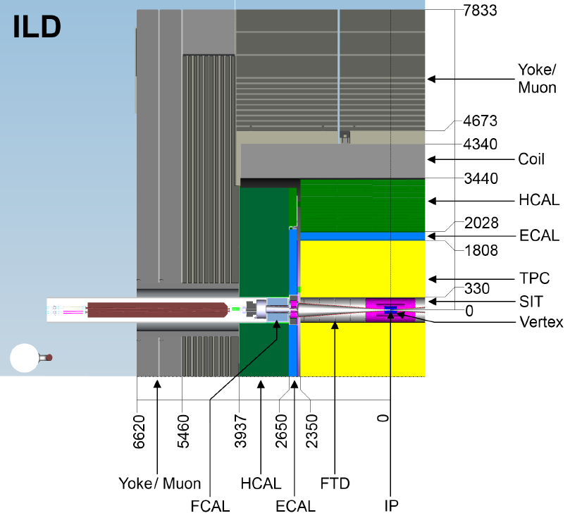
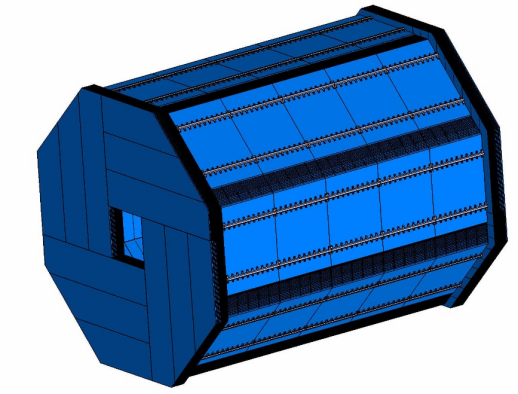
ECAL has an octagonal barrel part and two endcaps, as shown in Fig. 1, right. The former has 8 independent sides not touching each other. Every side is divided longitudinally along the beam axis into 5 modules attached to HCAL on common rails. One barrel module without active detector elements is shown in Fig 2, left.
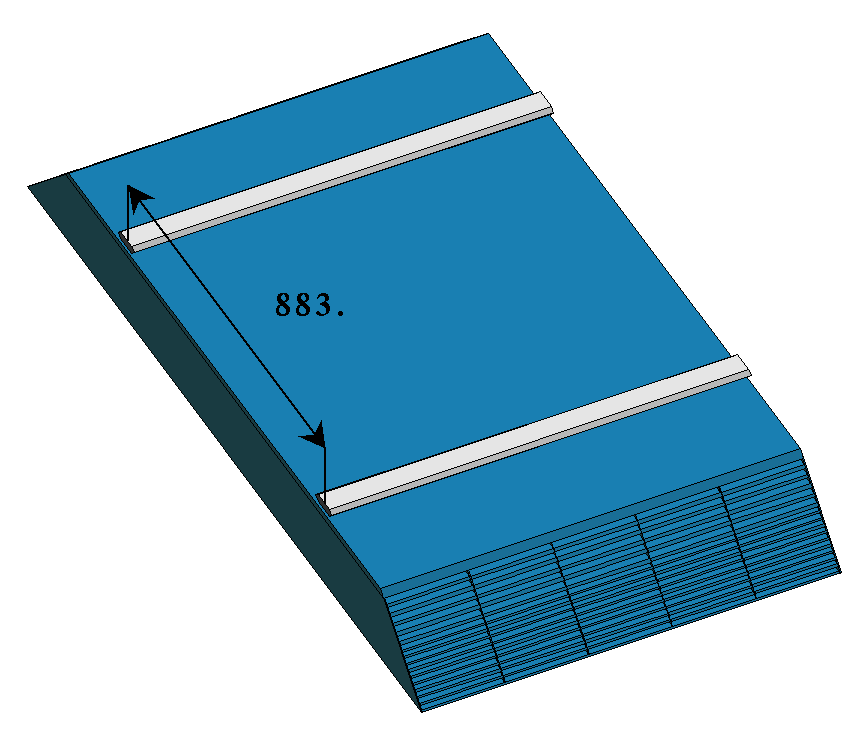
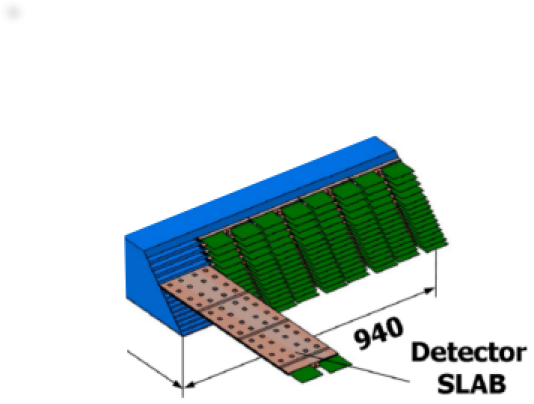
It is made of a carbon-fiber structure holding every second layer of the tungsten absorber. It has cavities called alveoli into which the active detectors called slabs slide in, as shown in Fig. 2, right.
The slabs carry in the middle the other layers of tungsten wrapped in carbon-fiber. Both sides of the absorber are equipped with the silicon matrices of PIN diode pixels and the front-end electronics. The silicon sensors are glued pixel-by-pixel to the readout printed circuit boards (PCBs) with a conductive epoxy. PCBs are connected in-line and read out from one slab end. All PCBs except the last one have a square shape. The endcaps are divided into 4 quadrants, each having 3 or 2 modules depending on the ILD size. The endcap modules are similar to the barrel ones but have a different shape, in particular, the slabs there are longer. In addition, the most forward ECAL endcap regions will be instrumented with the so-called ‘endcap rings” (not shown in Fig. 1). Their design is not yet finalized.
Currently, in addition to the ECAL with 30 layers described in the ILD TDR, there are design options with 22 layers, with 23% smaller radius and with thicker (725 m instead of 525 m) and larger silicon sensors made from 8 instead of 6 inch wafers.
2 CALICE physical and technological SiW ECAL prototypes
In 2004–2011 the first so-called “physical” prototype of SiW ECAL with 30 layers has been built and successfully tested within the CALICE collaboration [4]. It was designed to prove the physical PFA principles in beam tests. The electronics was not embedded inside the calorimeter but placed alongside.
After successful completion of the physical prototype program, the emphasis has moved to the technological realization of the detector scalable to the ILD ECAL. This second generation prototype is called “technological”. The electronics is embedded in the active layer. It is based on a dedicated 64 channel front-end chip SKIROC [5]. Since in the ILD there is no central trigger, every SKIROC chip has auto-trigger capabilities, and the full event is built using bunch crossing (BX) time stamps.
In the current design, the ILC collides bunch trains during 1 msec and then stays idle for 199 msec. The latter period is used to readout the data stored in SKIROC. To save the power and to simplify the cooling, the front-end electronics are switched off after each readout cycle. This is called "power pulsing". In such a mode one SKIROC channel consumes only about 27 . In practice, however, the electronics should be switched on about 1 msec before the bunch trains so that the transition processes (causing e.g. pedestal drifts) finish well in advance.
One PCB of the current prototype has 16 SKIROC chips and 1024 channels. It serves 4 silicon sensors each segmented into 256 pixels of 5.55.5 mm2 size. Up to now, seven such single PCB detectors have been built. They have been tested with cosmics, charge injection and in 3 beam test campaigns: at CERN in November 2015 and June 2016 and in DESY in June 2017. Every PCB was readout independently. In the test beams they formed a mini-ECAL with 7 layers. Overall, they have demonstrated a good performance [6, 7] though there is still some room for improvement of the readout electronics.
Single PCB detectors with size of about cm2 are called “short” slabs to distinguish them from multi-PCB “long” slabs required in the ILD. Their length, depending on the ILD size, can be as large as 1.5 m (2 m) in the barrel (endcap). This paper describes the R&D program aiming to build the first “long” slab prototype. Based on the learned experience from the “short” slabs, the current R&D is focused only on the performance of the readout electronics which is considered as the most difficult task. In particular, the future “long” slab prototype should verify:
-
•
clock and signal propagation along the “long” slab and their distortions,
-
•
low and high voltage distribution,
-
•
ability to read large data volumes and the integrity of data,
-
•
PCB electrical interconnections.
For simplicity, the prototype will leave out e.g. the ILD constraints on the sizes and the mechanical tolerances. Contrary to the ILD slab, the prototype will have no absorber and will have only one layer of PCB (the second should be identical).
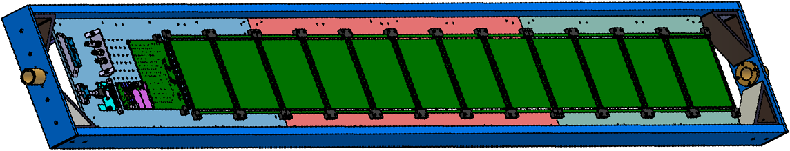
The scheme of the long slab prototype together with the holding mechanical structure is shown in Fig. 3. Up to 12 PCBs will be connected in-line. Similarly to the existing “short” slabs, the long slab will be communicated from one end via the so-called adapter and DIF boards, the latter being connected to the computer via a concentrator board GDCC (not shown). It will be possible to configure individually every chip of the prototype, for example, to perform individual masking of the channels.
In the “short” slabs, the interconnection between the PCB and the adapter board is performed by permanent soldering of a dedicated flexible flat kapton cable. The same method of interconnections is currently foreseen in the ILD for reliability. Here, due to a magnetic field there will be a Lorentz force acting on wires which feed currents to the front-end electronics. Due to the power pulsing, the currents will switch on and off at a frequency of 5 Hz. This will create vibrations, in particular, in the interconnections. The long slab prototype will not address the question of 100% reliability of the interconnections required for the ILD. For simplicity, the interconnections will be performed with Flat Flexible Cable (FFC) connectors. This will give the flexibility to freely connect and disconnect the PCBs which might be important for the future tests.
Each PCB will be equipped with one small silicon sensor having 4 pixels. This should be sufficient to study the physical performance of the detector. All 1024 channels of PCB will be checked with the charge injection.
The PCBs will be added to the long slab one-by-one, each time verifying the performance. In case of problems, the maximal allowed length of the current long slab prototype will be determined. Otherwise, the long slab will have 12 PCBs, as required for the endcap in the ILD with the maximal size. The base frame will contain 3 pieces, shown in Fig. 3 by different colors. By installing only one, two or all three pieces, one can vary the slab length, such as it can hold 2, 8 or 12 PCBs. The performance of the slab will be tested with Sr and Cs radioactive sources, cosmics, charge injection and in a beam test planned in 2018.
3 Current status of the ILD long slab prototype
The design of the long slab is finished. It can be rotated around its middle axis and fixed at any position. Vertical and horizontal orientations are foreseen for the beam and cosmic tests, respectively. The prototype length is 3.22 m, which is longer than the ILD slab because of the margins and an extra space needed for the current PCB interconnections. With the weight slightly less than 30 kg, the prototype can be handled by two people. The base frame is rigid. When held at two ends, the mechanical bending is less than 1 mm within one PCB area. The silicon sensor should be perfectly flat, therefore the PCB is fixed to the frame using a flexible support printed at a 3D printer. This prevents the bending to be propagated to the PCB and the sensor.
Access to the electronic boards is foreseen from both sides, the base frame has special holes under each PCB for that. The boards are electrically isolated to reduce noise. The prototype will be light-tight since the silicon detectors are sensitive to ambient light.
Even a small resistivity of low voltage (LV) power lines results in voltage drops due to large currents. They might become sizable at the far end of the slab (several hundred mV) if the power is distributed through the PCBs along the slab. Therefore, for simplicity, the PCBs will be powered not sequentially but by individual cables of the same length. There will be two such cables for LV and a ground, and their length will be determined by the last PCB at the slab end.
The high voltage (HV) will be supplied to the silicon sensors by a separate cable glued at one end to a HV pad of the sensor. The other end will be possible to disconnect from a HV source, if it will be necessary to change the PCB with the sensor.
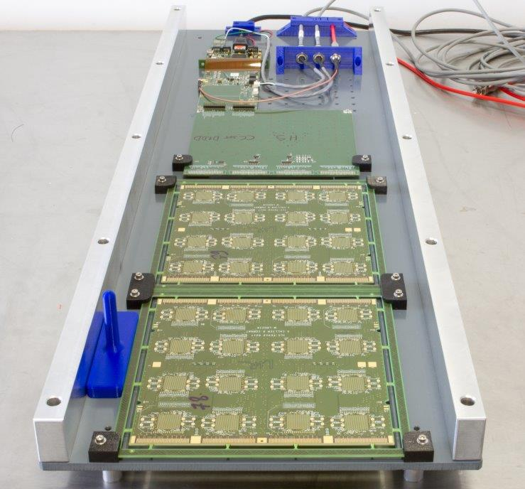
The first two PCBs with the glued small sensors have been already installed in the long slab prototype (see Fig. 4) and prepared for the first tests. All other PCBs and sensors are available. They will be installed one-by-one and tested. The full long slab prototype is due in the beginning of March 2018.
4 Conclusions
In this paper we have described the plans and the first steps to build the first prototype of the ILD SiW ECAL detector element with up to 12 288 channels. It will contain up to 12 PCBs connected in-line and forming the so-called “long” slab. The main focus is on the electronics readout which is considered as the most difficult part of the R&D. The prototype will be controlled and read out from one end using existing adapter, DIF and GDCC boards. Every PCB has 16 SKIROC chips and 1024 channels. It will be equipped with the small silicon sensor with pixels. This should be sufficient to check the physical performance of the prototype. The other channels will be checked with the charge injection available in SKIROC.
The first part of the prototype with 2048 channels have been already built. The full prototype is due in the beginning of 2018.
Acknowledgments
Supported by the H2020 project AIDA-2020, GA no. 654168.
References
- [1] J.-C. Brient, H. Videau, The calorimetry at the future linear collider, proccedings of APS/DPF/DBP Summer Study on the Future of Particle Physics (Snowmass, Colorado, 2002), arXiv:hep-ex/0202004.
- [2] M.A. Thomson, Particle flow calorimetry and the PandoraPFA algorithm, NIM A611 (2009) 25, arXiv:0907.3577.
- [3] A. Abada et al., The International Linear Collider Technical Design Report - Volume 4: Detectors (2013), arxiv:1306.6329.
- [4] J.Repond et al., Design and Electronics Commissioning of the Physics Prototype of a Si-W Electromagnetic Calorimeter for the International Linear Collider, JINST 3 (2008) P08001, arXiv:0805.4833.
- [5] S Callier et al., SKIROC2, front end chip designed to readout the Electromagnetic CALorimeter at the ILC, JINST 6 (2011) C12040.
- [6] V. Balagura et al., SiW ECAL for future e+e- collider, JINST 12 (2017), no.07, C07013, arXiv:1705.10838.
- [7] A. Irles, Latest R&D news and beam test performance of the highly granular SiW-ECAL technological prototype for the ILC, report at this conference.