Large spin relaxation anisotropy and valley-Zeeman spin-orbit coupling in WSe2/Gr/hBN heterostructures
Abstract
Large spin-orbital proximity effects have been predicted in graphene interfaced with a transition metal dichalcogenide layer. Whereas clear evidence for an enhanced spin-orbit coupling has been found at large carrier densities, the type of spin-orbit coupling and its relaxation mechanism remained unknown. We show for the first time an increased spin-orbit coupling close to the charge neutrality point in graphene, where topological states are expected to appear. Single layer graphene encapsulated between the transition metal dichalcogenide WSe2 and hBN is found to exhibit exceptional quality with mobilities as high as . At the same time clear weak anti-localization indicates strong spin-orbit coupling and a large spin relaxation anisotropy due to the presence of a dominating symmetric spin-orbit coupling is found. Doping dependent measurements show that the spin relaxation of the in-plane spins is largely dominated by a valley-Zeeman spin-orbit coupling and that the intrinsic spin-orbit coupling plays a minor role in spin relaxation. The strong spin-valley coupling opens new possibilities in exploring spin and valley degree of freedom in graphene with the realization of new concepts in spin manipulation.
I Motivation/Introduction
In recent years, van der Waals heterostructures (vdW) have gained a huge interest due to their possibility of implementing new functionalities in devices by assembling 2D building blocks on demand 2013_Geim . It has been shown that the unique band structure of graphene can be engineered and enriched with new properties by placing it in proximity to other materials, including the formation of minibands 2013_Ponomarenko ; 2013_Dean ; 2013_Hunt ; 2016_lee , magnetic ordering 2015_Wang_b ; 2017_Leutenantsmeyer , and superconductivity 2015_Efetov ; 2017_Bretheau . Special interest has been paid to the enhancement of spin-orbit coupling (SOC) in graphene since a topological state, a quantum spin Hall phase, was theoretically shown to emerge 2005_Kane . First principles calculations predicted an intrinsic SOC strength of 2010_Konschuh , which is currently not observable even in the cleanest devices. Therefore, several routes were proposed and explored to enhance the SOC in graphene while preserving its high electronic quality 2009_CastroNeto ; 2014_Han ; 2015_Gmitra . One of the most promising approaches is the combination of a transition metal dichalcogenide (TMDC) layer with graphene in a vdW-hetereostructure. TMDCs have very large SOC on the –scale in the valence band and large SOC on the order of in the conduction band 2014_Han .
The realization of topological states is not the only motivation to enhance the SOC in graphene. It has been shown that graphene is an ideal material for spin transport 2014_Han . Spin relaxation times on the order of nanoseconds 2014_Droegeler ; 2016_Singh and relaxation lengths of 2015_Ingla-Aynes have been observed. However, the presence of only weak SOC in pristine graphene limits the tunability of possible spintronics devices made from graphene. The presence of strong SOC would enable fast and efficient spin manipulation by electric fields for possible spintronics applications, such as spin-filters 2017_Cummings or spin-orbit valves 2017_Gmitra ; 2017_Khoo . In addition, enhanced SOC leads to large spin-Hall angles 2017_Garcia that could be used as a source of spin currents or as a detector of spin currents in graphene-based spintronic devices.
It was proposed that graphene in contact to a single layer of a TMDC can inherit a substantial SOC from the underlying substrate 2015_Gmitra ; 2016_Gmitra . The experimental detection of clear weak anti-localization (WAL) 2015_Wang_a ; 2016_Wang ; 2016_Yang ; 2017_Voelkl ; 2017_Yang ; 2017_Wakamura as well as the observation of a beating of Shubnikov de-Haas (SdH) oscillations 2016_Wang leave no doubt that the SOC is greatly enhanced in graphene/TMDC heterostructures. First principles calculations of graphene on WSe2 2016_Gmitra predicted large spin-orbit coupling strength and the formation of inverted bands hosting special edge states. At low energy, the band structure can be described in a simple tight-binding model of graphene containing the orbital terms and all the symmetry allowed SOC terms 2016_Gmitra ; 2017_Kochan :
| (1) | ||||
Here, are the Pauli matrices acting on the pseudospin, are the Pauli matrices acting on the real spin and is either and denotes the valley degree of freedom. and represent the k-vector in the graphene plane, is the reduced Planck constant, is the Fermi velocity and are constants. The first term is the usual graphene Hamiltonian that describes the linear band structure at low energies. represents an orbital gap that arises from a staggered sublattice potential. is the intrinsic SOC term that opens a topological gap of 2005_Kane . is a valley-Zeeman SOC that couples valley to spin and results from different intrinsic SOC on the two sublattices. This term leads to a Zeeman splitting of that has opposite sign in the K and K’ valleys and leads to an out of plane spin polarization with opposite polarization in each valley. is a Rashba SOC arising from the structure inversion asymmetry. This term leads to a spin splitting of the bands with a spin expectation value that lies in the plane and is coupled to the momentum via the pseudospin. At higher energies k-dependent terms, called pseudospin inversion asymmetric (PIA) SOC come into play, which can be neglected at lower doping 2017_Kochan .
Previous studies have estimated the SOC strength from theoretical calculations 2015_Wang_a or extracted only the Rashba SOC at intermediate 2017_Yang or at very high doping 2016_Yang or gave only a total SOC strength 2017_Voelkl . Further studies have extracted a combination of Rashba and valley-Zeeman SOC strength form SdH-oscillation beating measurements 2016_Wang . Additionally, a very recent study uses the clean limit (precession time) to estimate the SOC strength from diffusive WAL measurements 2017_Wakamura .
Here, we give for the first time a clear and comprehensive study of SOC at the charge neutrality point (CNP) for WSe2/Gr/hBN heterostructures. The influence of strong SOC is expected to have the largest impact on the bandstructure close to the CNP. The strength of all possible SOC terms is discussed and we find that the relaxation times are dominated by the valley-Zeeman SOC. The valley-Zeeman SOC leads to a much faster relaxation of in-plane spins than out-of plane spins. This asymmetry is unique for systems with strong valley-Zeeman SOC and is not present in traditional 2D Rashba systems where the anisotropy is 1/2 2017_Cummings . Our study is in contrast to previous WAL measurements 2016_Yang ; 2017_Yang , but is in good agreement with recent spin-valve measurements reporting a large spin relaxation anisotropy 2017_Ghiasi ; 2017_Benitez .
II Methods
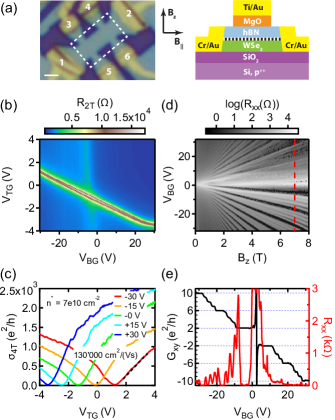
WSe2/Gr/hBN vdW-heterostructures were assembled using a dry pick-up method 2014_Zomer and Cr/Au 1D-edge contacts were fabricated 2013_Wang_a . Obviously a clean interface between high quality WSe2 and graphene is of utmost importance. A short discussion on the influence of the WSe2 quality is given in the Supplemental Material. After shaping the vdW-heterostructure into a Hall-bar geometry by a reactive ion etching plasma employing SF6 as the main reactive gas, Ti/Au top gates were fabricated with an MgO dielectric layer to prevent it from contacting the exposed graphene at the edge of the vdW-heterostructure. A heavily-doped silicon substrate with SiO2 was used as a global back gate. An optical image of a typical device and a cross section is shown in Fig. 1 (a). In total, three different samples with a total of four devices were fabricated. Device A, B and C are presented in the main text and device D is discussed in the Supplemental Material. Standard low frequency lock-in techniques were used to measure two- and four-terminal conductance and resistance. Weak anti-localization was measured at temperatures of to whereas a classical background was measured at sufficiently large temperatures of .
III Results
III.1 Device Characterization
The two-terminal resistance measured from contact 1 to 2 as a function of applied top and bottom gate is shown in Fig. 1 (b). A pronounced resistance maximum, tunable by both gates, indicates the CNP of the bulk of the device whereas a fainter line only changing with VBG indicates the CNP from the device areas close to the contacts, which are not covered by the top gate. From the four-terminal conductivity, shown in Fig. 1 (c), the field effect mobility and the residual doping = were extracted. The mobility was extracted from a linear fit of the conductivity as a function of density at negative VBG. At positive VBG the mobility is higher as one can easily see from Fig. 1 (c). At , the lever arm of the back gate is greatly reduced since the WSe2 layers gets populated with charge carriers, i.g. the Fermi level is shifted into some trap states in the WSe2. Although the WSe2 is poorly conducting (low mobility) it can screen potential fluctuations due to disorder and this can lead to a larger mobility in the graphene layer, as similarly observed in graphene on MoS2 2017_Banszerus .
Fig. 1 (d) shows the longitudinal resistance as a function of magnetic field and gate voltage with lines originating from the integer quantum Hall effect. At low fields, the normal single layer spectrum is obtained with plateaus at filling factors , whereas at larger magnetic fields full degeneracy lifting is observed with plateaus at filling factors . The presence of symmetry broken states, that are due to electron-electron interactions 2012_Young , is indicative of a high device quality. In the absence of interaction driven symmetry breaking, the spin-splitting of the quantum Hall states could be used to investigate the SOC strength 2017_Cysne .
The high quality of the devices presented here poses sever limitations on the investigation of the SOC strength using WAL theory. Ballistic transport features (transverse magnetic focusing) are observed at densities larger than . Therefore, a true diffusive regime is only obtained close to the CNP, where the charge carriers are quasi-diffusive 2011_DasSarma .
III.2 Magneto conductance
In a diffusive conductor, the charge carrier trajectories can form closed loops after several scattering events. The presence of time-reversal symmetry leads to a constructive interference of the electronic wave function along these trajectories and therefore to an enhanced back scattering probability compared to the classical case. This phenomenon is known as weak localization (WL). Considering the spin degree of freedom of the electrons, this can change. If strong SOC is present the spin can precess between scattering events, leading to destructive interference and hence to an enhanced forward scattering probability compared to the classical case. This phenomenon is known as weak anti-localization 1982_Bergmann . The quantum correction to the magneto conductivity can therefore reveal the SOC strength.
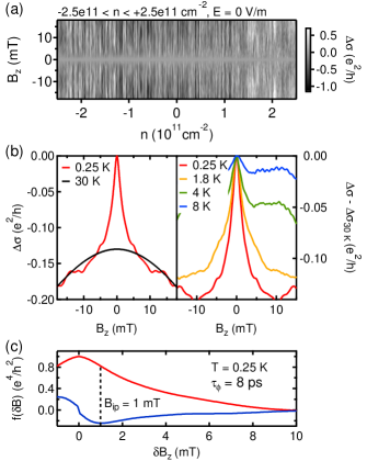
The two-terminal magneto conductivity versus Bz and n at T = and zero perpendicular electric field is shown in Fig. 2 (a). A clear feature at Bz = is visible, as well as large modulations in Bz and n due to universal conductance fluctuations (UCFs). UCFs are not averaged out since the device size is on the order of the dephasing length . Therefore, an ensemble average of the magneto conductivity over several densities is performed to reduce the amplitude of the UCFs 2015_Wang_a , and curves as in Fig. 2 (b) result. A clear WAL peak is observed at whereas at the quantum correction is fully suppressed due to a very short phase coherence time and only a classical background in magneto conductivity remains. This high temperature background is then subtracted from the low temperature measurements to extract the real quantum correction to the magneto conductivity 2016_Wang . In addition to WL/WAL measurements the phase coherence time can be extracted independently from the autocorrelation function of UCF in magnetic field 1987_Lee . UCF as a function of Bz was measured in a range where the WAL did not contribute to the magneto conductivity (e.g. ) and an average over several densities was performed. The inflection point in the autocorrelation, determined by the minimum in its derivative, is a robust measure of 2012_Lundeberg , see Fig. 2 (d).
III.3 Fitting
To extract the spin-orbit scattering times we use the theoretical formula derived by diagrammatic perturbation theory 2012_McCann . In the case of graphene, the quantum correction to the magneto conductivity in the presence of strong SOC is given by:
| (2) |
where , with being the digamma function, , where is the diffusion constant, is the phase coherence time, is the spin-orbit scattering time due to SOC terms that are asymmetric upon z/-z inversion () and is the spin-orbit scattering time due to SOC terms that are symmetric upon z/-z inversion (, ) 2012_McCann . The total spin-orbit scattering time is given by the sum of the asymmetric and symmetric rate . In general, Eq. 2 is only valid if the intervalley scattering rate is much larger than the dephasing rate and the rates due to spin-orbit scattering , .
In the limit of very weak asymmetric but strong symmetric SOC (), Eq. 2 describes reduced WL since the first two terms cancel and therefore a positive magneto conductivity results. Contrary to that, in the limit of very weak symmetric but strong asymmetric SOC () a clear WAL peak is obtained. If both time scales are shorter than , the ratio will determine the quantum correction of the magneto conductivity. In the limit of total weak SOC () the normal WL in graphene is obtained 2006_McCann , as the first two terms cancel and other terms explicitly involving the inter- and intravalley scattering must be considered (see Supplemental Material).
Since the second and the third term can produce very similar dependencies on Bz it can be hard to properly distinguish between the influence of and on , as also previously reported 2016_Wang ; 2017_Wakamura . It is therefore important to measure and fit the magneto conductivity to sufficiently large fields in order to capture the influence of the second and third term, which only significantly contribute at larger fields (for strong SOC). However, there is an upper limit of the field scale (the so-called transport field ) at which the theory of WAL breaks down. The size of the shortest closed loops that can be formed in a diffusive sample is on the order of , where is the mean-free path of the charge carriers. Fields that are larger than , where is the flux quantum, are not meaningful in the framework of diffusive transport.
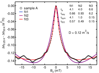
In the most general case there are three different regimes in the presence of strong SOC in graphene: , and . Therefore, we fitted the magneto conductivity with initial fit parameters in these three limits. An example is shown in Fig. 3, where the three different fits are shown as well as the extracted parameters. Obviously, the case (fit1) and (fit2) are indistinguishable and fit the data worse than the case (fit3). In addition, extracted from the UCF matches best for fit3. Therefore, we can clearly state that the symmetric SOC is stronger than the asymmetric SOC. The flat background as well as the narrow width of the WAL peak can only be reproduced with the third case. A very similar behaviour was found in device C at the CNP. In device B (shown in the Supplemental Material), whose mobility is larger than the one from device A, we cannot clearly distinguish the three limits as the transport field is too low ( ) and the flat background at larger field cannot be used to disentangle the different parameters from each other. However, this does not contradict and the overall strength of the SOC ( ) is in good agreement with device A shown here.
Obviously, the extracted time scales should be taken with care as many things can introduce uncertainties in the extracted time scales. First of all, we are looking at ensemble-averaged quantities and it is clear that this might influence the precision of the extraction of the time scales. In addition, the subtraction of a high temperature background can lead to higher uncertainty of the quantum correction. Lastly, the high mobility of the clean devices places severe limitations on the usable range of magnetic field. All these influences lead us to a conservative estimation of a uncertainty for the extracted time scales. Nevertheless, the order of magnitude of the extracted time scales and trends are still robust.
The presence of a top and a back gate allows us to tune the carrier density and the transverse electric field independently. The spin-orbit scattering rates were found to be electric field independent at the CNP in the range of within the precision of parameter extraction. Details are given in the Supplemental Material. Within the investigated electric field range was found to be in the range of , always close to . on the other hand was found to be around while was around , see Supplemental Material for more details. The lack of electric field tunability of and in the investigated electric field range is not so surprising. The Rashba coupling in this system is expected to change considerably for electric fields on the order of , which are much larger than the applied fields here. However, such large electric fields are hard to achieve. In addition, , which results from and is not expected to change much with electric field as long as the Fermi energy is not shifted into the conduction or valence band of the WSe2 2015_Gmitra . These findings contradict another study 2017_Voelkl , which claims an electric field tunability of both SOC terms. However, there it is not discussed how accurately those parameters were extracted.
III.4 Density dependence
The momentum relaxation time can be tuned by changing the carrier density in graphene. Fig. 4 shows the dependence of and on in a third device C. The lower mobility in device C allowed for WAL measurements at higher charge carrier densities not accessible in devices A and B. At the CNP, and are found to be consistent across all three devices A, B and C. Here, increases with increasing whereas is roughly constant with increasing . The dependence of the spin-orbit scattering times on the momentum scattering time can give useful insights into the dominating spin relaxation mechanisms, as will be discussed later. It is important to note that the extracted is always very close to . Therefore, the extracted could be shorter than what the actual value would be since acts as a cutoff.

III.5 In-plane magnetic field dependence
An in-plane magnetic field (B∥) is expected to lift the influence of SOC on the quantum correction to the magneto conductivity at sufficiently large fields. This means that a crossover from WAL to WL for z/-z asymmetric and a crossover from reduced WL to full WL correction for z/-z symmetric spin-orbit coupling is expected at a field where the Zeeman energy is much larger than the SOC strength 2012_McCann . The experimental determination of this crossover field allows for an estimate of the SOC strength.
The B∥ dependence of the quantum correction to the magneto conductivity of device A at the CNP and at zero perpendicular electric field was investigated, as shown in Fig. 5. The WAL peak decreases and broadens with increasing B∥ until it completely vanishes at B. Neither a reappearance of the WAL peak, nor a transition to WL, is observed at higher B∥ fields (up to ). A qualitatively similar behaviour was observed for device D. Fits with equation 2 allow the extraction of and , which are shown in Fig. 5 (b) for B∥ fields lower than . A clear decrease of is observed while remains constant.
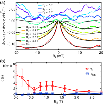
The reduction in with increasing B∥ was previously attributed to enhanced dephasing due to a random vector potential created by a corrugated graphene layer in an in-plane magnetic field 2010_Lundeberg . The clear reduction in with constant and the absence of any appearance of WL at larger B∥ also strongly suggests that a similar mechanism is at play here. Therefore, the vanishing WAL peak is due to the loss of phase coherence and not due to the fact that the Zeeman energy () is exceeding the SOC strength. Using the range where WAL is still present, we can define a lower bound of the crossover field when drops below of its initial value, which corresponds to here. This leads to a lower bound of the SOC strength given a g-factor of 2.
IV Discussion
The effect of SOC was investigated in high quality vdW-heterostructures of WSe2/Gr/hBN at the CNP, as there the effects of SOC are expected to be most important. The two-terminal conductance measurements are not influenced by contact resistances nor pn-interfaces close to the CNP. At larger doping, the two-terminal conductance would need to be considered with care.
Phase coherence times around were consistently found from fits to Eq. 2 and from the autocorrelation of UCF. It is commonly known that the phase coherence time is shorter at the CNP than at larger doping 2008_Tikhonenko ; 2010_Lundeberg . Moreover, large diffusion coefficients lead to long phase coherence lengths being on the order of the device size ( ), which in turn leads to large UCF amplitudes making the analysis harder.
In general Eq. 2 is only applicable for short . Since is unknown in these devices, only an estimate can be given here. WL measurements of graphene on hBN found on the order of picoseconds own_WL_measurement ; 2014_Couto . Inter-valley scattering is only possible at sharp scattering centres as it requires a large momentum change. It is a reasonable assumption that the defect density in WSe2, which is around 2016_Addou , is larger than in the high quality hBN 2007_Taniguchi . This leads to shorter times in graphene placed on top of WSe2 and makes Eq. 2 applicable despite the short spin-orbit scattering times found here. In the case of weaker SOC, Eq. 2 cannot be used. Instead, a more complex analysis including and is needed. This was used for device D, and is presented in the Supplemental Material.
Spin-orbit scattering rates were successfully extracted at the CNP and was found to be around whereas was found to be much shorter, around . In these systems, if is sufficiently short, is predicted to represent the out-of-plane spin relaxation time and then represents the in-plane spin relaxation time 2017_Cummings . For the time scales stated above, a spin relaxation anisotropy is found (see Supplemental Material for detailed calculation). This large anisotropy in spin relaxation is unique for systems with a strong valley-Zeeman SOC. Similar anisotropies have been found recently in spin valves in similar systems 2017_Ghiasi ; 2017_Benitez .
In order to link spin-orbit scattering time scales to SOC strengths, spin relaxation mechanisms have to be considered. The simple definition of as the SOC strength is only valid in the limit where the precession frequency is much larger than the momentum relaxation rate (e.g. full spin precession occurs between scattering events). In the following we concentrate on the parameters from device A that were extracted close to the CNP. The dependence on in device A can most likely be assumed to be very similar to that observed in device C. Within the investigated density range of , including residual doping, an average Fermi energy of was estimated. This is based on the density of states of pristine graphene, which should be an adequate assumption for a Fermi energy larger than any SOC strengths.
The symmetric spin-orbit scattering time contains contributions from the intrinsic SOC and from the valley-Zeeman SOC. Up to now, only the intrinsic SOC has been considered in the analysis of WAL measurements, and the impact of valley-Zeeman SOC has been ignored. However, as we now explain, it is highly unlikely that intrinsic SOC is responsible for the small values of . The intrinsic SOC is expected to relax spin via the Elliott-Yafet (EY) mechanism 2012_Ochoa , which is given as
| (3) |
where is the spin relaxation time, is the Fermi energy, is the intrinsic SOC strength and is the momentum relaxation time 2012_Ochoa . Since the intrinsic SOC does not lead to spin-split bands and hence no spin-orbit fields exist that could lead to spin precession, a relaxation via the Dyakonov-Perel mechanism can be excluded. Therefore, we can estimate using , a mean Fermi energy of and a momentum relaxation time of . The extracted value for would correspond to the opening of a topological gap of . In the presence of a small residual doping (here ), such a large topological gap should easily be detectable in transport. However, none of our transport measurements confirm this. In addition, the increase of with , as shown in Fig. 4, does not support the EY mechanism.
On the other hand, Cummings et al. have shown that the in-plane spins are also relaxed by the valley-Zeeman term via a Dyakonov-Perel mechanism where takes the role of the momentum relaxation time 2017_Cummings :
| (4) |
While this equation applies in the motional narrowing regime of spin relaxation, our measurement appears to be near the transition where that regime no longer applies. Taking this into consideration (see Supplemental Material), we estimate to be in the range of for a of and a of . This agrees well with first principles calculations 2016_Gmitra . The large range in comes from the fact that is not exactly known.
Obviously, could still contain parts that are related to the intrinsic SOC ( ). As an upper bound of , we can give a scale of , which corresponds to half the energy scale due to the residual doping in the system. This would lead to . Such a slow relaxation rate () is completely masked by the much larger relaxation rate coming from the valley-Zeeman term. Therefore, the presence of the valley-Zeeman term makes it very hard to give a reasonable estimate of the intrinsic SOC strength.
The asymmetric spin-orbit scattering time contains contributions from the Rashba-SOC and from the PIA SOC. Since the PIA SOC scales linearly with the momentum, it can be neglected at the CNP. Here, represents only the spin-orbit scattering time coming from Rashba SOC. It is known that Rashba SOC can relax the spins via the Elliott-Yafet mechanism 2012_Ochoa . In addition, the Rashba SOC leads to a spin splitting of the bands and therefore to a spin-orbit field. This opens a second relaxation channel via the Dyakonov-Perel mechanism 1972_Dyakonov . In principle the dependence on the momentum scattering time allows one to distinguish between these two mechanisms. Here, does not monotonically depend on as one can see in Fig. 4 and therefore we cannot unambiguously decide between the two mechanisms.
Assuming that only the EY mechanism is responsible for spin relaxation, then can be estimated, using of , a mean Fermi energy of and a momentum relaxation time of . On the other hand, pure DP-mediated spin relaxation leads to . The Rashba SOC strength estimated by the EY relaxation mechanism is large compared to first principles calculations 2016_Gmitra , which agree much better with the SOC strength estimated by the DP mechanism. This is also in agreement with previous findings 2016_Yang ; 2017_Yang .
Since there is a finite valley-Zeeman SOC, which is a result of different intrinsic SOC on the A sublattice and B sublattice, a staggered sublattice potential can also be expected. The presence of a staggered potential, meaning that the on-site energy of the A atom is different from the B atom on average, leads to the opening of a trivial gap of at the CNP. Since there is no evidence of an orbital gap, we take the first principles calculations as an estimate of .
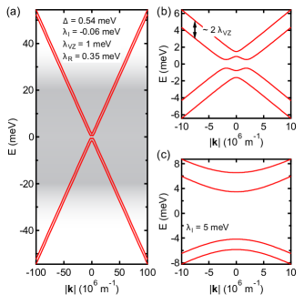
Knowing all relevant parameters in Eq. 1, a band structure can be calculated, which is shown in Fig. 6. The bands are spin split mainly due to the presence of strong valley-Zeeman SOC but also due to the weaker Rashba SOC. At very low energies, an inverted band is formed due to the interplay of the valley-Zeeman and Rashba SOC, see Fig. 6 (b). This system was predicted to host helical edge states for zigzag graphene nanoribbons, demonstrating the quantum spin Hall effect 2016_Gmitra . In the case of stronger intrinsic SOC, which we cannot estimate accurately, a band structure as in Fig. 6 (c) is expected with a topological gap appearing at low energies. We would like to note here, that this system might host a quantum spin Hall phase. However, its detection is still masked by device quality as the minimal Fermi energy is much larger than the topological gap, see also Fig. 6 (a).
Our findings are in good agreement with the calculations by Gmitra et al. 2016_Gmitra . However, we have to remark that whereas the calculations were performed for single-layer TMDCs, we have used multilayer WSe2 as a substrate. Single-layer TMDCs are direct band-gap semiconductors with the band gap located at the K-point whereas multilayer TMDCs have an indirect band gap. Since the SOC results from the mixing of the graphene orbitals with the WSe2 orbitals, the strength of the induced SOC depends on the relative band alignment between the graphene and WSe2 band, which will be different for single- or multilayer TMDCs. This difference was recently shown by Wakamura et al. 2017_Wakamura . Therefore using single-layer WSe2 to induce SOC might even enhance the coupling found by our studies. Furthermore, the parameters taken from Ref. 2016_Gmitra for the orbital gap and for the intrinsic SOC therefore have to be taken with care.
V Conclusion
In conclusion we measured weak anti-localization in high quality WSe2/Gr/hBN vdW-heterostructures at the charge neutrality point. The presence of a clear WAL peak reveals a strong SOC with a much faster spin relaxation of in-plane spins compared to out-of-plane spins. Whereas previous studies have also found a clear WAL signal, we present for the first time a complete interpretation of all involved SOC terms considering their relaxation mechanisms. This includes the finding of a very large spin relaxation anisotropy that is governed by the presence of a valley-Zeeman SOC that couples spin to valley. The relaxation mechanism at play here is very special since it relies on intervalley scattering and can only occur in materials where a valley degree of freedom is present and coupled to spin. This is in excellent good agreement with recent spin-valve measurements that found also very large spin relaxation anisotropies in similar systems 2017_Ghiasi ; 2017_Benitez .
In addition, we investigated the influence of an in-plane magnetic field on the WAL signature. Due to the loss of phase coherence, a lower bound of all SOC strengths of can be given, which is in agreement with the numbers presented above. This approach does not depend on accurate fitting of WAL peaks nor on the interpretation of spin-orbit scattering rates.
The coupling of spin and valley opens new possibilities in exploring spin and valley degrees of freedom in graphene. In the case of bilayer graphene in proximity to WSe2 an enormous gate tunability of the SOC strength is predicted since full layer polarization can be achieved by an external electric field 2017_Gmitra ; 2017_Khoo . This is just one of many possible routes to investigate in the future.
Acknowledgments
The authors gratefully acknowledge fruitful discussions on the interpretation of the experimental data with Martin Gmitra and Vladimir Fal’ko. Clevin Handschin is acknowledged for helpful discussions on the sample fabrication. This work has received funding from the European Union’s Horizon 2020 research and innovation programme under grant agreement No 696656 (Graphene Flagship), the Swiss National Science Foundation, the Swiss Nanoscience Institute, the Swiss NCCR QSIT and ISpinText FlagERA network OTKA PD-121052 and OTKA FK-123894. P.M. acknowledges support as a Bolyai Fellow. ICN2 is supported by the Severo Ochoa program from Spanish MINECO (Grant No. SEV-2013-0295) and funded by the CERCA Programme / Generalitat de Catalunya.
Author contributions S.Z. fabricated and measured the devices with the help of P.M. K.M. contributed to the fabrication of device C. S.Z. analysed the data with help from P.M. and inputs from C.S.. S.Z., P.M., A.W.C., J.H.G and C.S. were involved in the interpretation of the results. S.Z. wrote the manuscript with inputs from P.M., C.S., A.W.C. and J.H.G., K.W. and T.T. provided the hBN crystals used in the devices.
References
- (1) A. K. Geim and I. V. Grigorieva. Van der Waals heterostructures. Nature, 499(7459):419–425, July 2013.
- (2) L. A. Ponomarenko, R. V. Gorbachev, G. L. Yu, D. C. Elias, R. Jalil, A. A. Patel, A. Mishchenko, A. S. Mayorov, C. R. Woods, J. R. Wallbank, M. Mucha-Kruczynski, B. A. Piot, M. Potemski, I. V. Grigorieva, K. S. Novoselov, F. Guinea, V. I. Fal’ko, and A. K. Geim. Cloning of Dirac fermions in graphene superlattices. Nature, 497:594–, May 2013.
- (3) C. R. Dean, L. Wang, P. Maher, C. Forsythe, F. Ghahari, Y. Gao, J. Katoch, M. Ishigami, P. Moon, M. Koshino, T. Taniguchi, K. Watanabe, K. L. Shepard, J. Hone, and P. Kim. Hofstadter’s butterfly and the fractal quantum Hall effect in moiré superlattices. Nature, 497:598–, May 2013.
- (4) B. Hunt, J. D. Sanchez-Yamagishi, A. F. Young, M. Yankowitz, B. J. LeRoy, K. Watanabe, T. Taniguchi, P. Moon, M. Koshino, P. Jarillo-Herrero, and R. C. Ashoori. Massive Dirac Fermions and Hofstadter Butterfly in a van der Waals Heterostructure. Science, 340(6139):1427–1430, 2013.
- (5) Menyoung Lee, John R. Wallbank, Patrick Gallagher, Kenji Watanabe, Takashi Taniguchi, Vladimir I. Fal’ko, and David Goldhaber-Gordon. Ballistic miniband conduction in a graphene superlattice. Science, 353(6307):1526–1529, 2016.
- (6) Zhiyong Wang, Chi Tang, Raymond Sachs, Yafis Barlas, and Jing Shi. Proximity-Induced Ferromagnetism in Graphene Revealed by the Anomalous Hall Effect. Phys. Rev. Lett., 114:016603, Jan 2015.
- (7) Johannes Christian Leutenantsmeyer, Alexey A Kaverzin, Magdalena Wojtaszek, and Bart J van Wees. Proximity induced room temperature ferromagnetism in graphene probed with spin currents. 2D Materials, 4(1):014001, 2017.
- (8) D. K. Efetov, L. Wang, C. Handschin, K. B. Efetov, J. Shuang, R. Cava, T. Taniguchi, K. Watanabe, J. Hone, C. R. Dean, and P. Kim. Specular interband Andreev reflections at van der Waals interfaces between graphene and NbSe2. Nature Physics, 12:328–, December 2015.
- (9) Landry Bretheau, Joel I-Jan Wang, Riccardo Pisoni, Kenji Watanabe, Takashi Taniguchi, and Pablo Jarillo-Herrero. Tunnelling spectroscopy of Andreev states in graphene. Nature Physics, 13:756–, May 2017.
- (10) C. L. Kane and E. J. Mele. Quantum Spin Hall Effect in Graphene. Phys. Rev. Lett., 95:226801, Nov 2005.
- (11) Sergej Konschuh, Martin Gmitra, and Jaroslav Fabian. Tight-binding theory of the spin-orbit coupling in graphene. Phys. Rev. B, 82:245412, Dec 2010.
- (12) A. H. Castro Neto and F. Guinea. Impurity-Induced Spin-Orbit Coupling in Graphene. Phys. Rev. Lett., 103:026804, Jul 2009.
- (13) Wei Han, Roland K. Kawakami, Martin Gmitra, and Jaroslav Fabian. Graphene spintronics. Nat Nano, 9(10):794–807, October 2014.
- (14) Martin Gmitra and Jaroslav Fabian. Graphene on transition-metal dichalcogenides: A platform for proximity spin-orbit physics and optospintronics. Phys. Rev. B, 92:155403, Oct 2015.
- (15) Marc Drögeler, Frank Volmer, Maik Wolter, Bernat Terrés, Kenji Watanabe, Takashi Taniguchi, Gernot Güntherodt, Christoph Stampfer, and Bernd Beschoten. Nanosecond Spin Lifetimes in Single- and Few-Layer Graphene-hBN Heterostructures at Room Temperature. Nano Letters, 14(11):6050–6055, 2014. PMID: 25291305.
- (16) Simranjeet Singh, Jyoti Katoch, Jinsong Xu, Cheng Tan, Tiancong Zhu, Walid Amamou, James Hone, and Roland Kawakami. Nanosecond spin relaxation times in single layer graphene spin valves with hexagonal boron nitride tunnel barriers. Applied Physics Letters, 109(12):122411, 2016.
- (17) J. Ingla-Aynés, Marcos H. D. Guimarães, Rick J. Meijerink, Paul J. Zomer, and Bart J. van Wees. 24 m length spin relaxation length in boron nitride encapsulated bilayer graphene. arXiv:1506.00472, 2015.
- (18) Aron W. Cummings, Jose H. Garcia, Jaroslav Fabian, and Stephan Roche. Giant Spin Lifetime Anisotropy in Graphene Induced by Proximity Effects. Phys. Rev. Lett., 119:206601, Nov 2017.
- (19) Martin Gmitra and Jaroslav Fabian. Proximity Effects in Bilayer Graphene on Monolayer : Field-Effect Spin Valley Locking, Spin-Orbit Valve, and Spin Transistor. Phys. Rev. Lett., 119:146401, Oct 2017.
- (20) Jun Yong Khoo, Alberto F. Morpurgo, and Leonid Levitov. On-Demand Spin–Orbit Interaction from Which-Layer Tunability in Bilayer Graphene. Nano Letters, 17(11):7003–7008, 2017. PMID: 29058917.
- (21) Jose H. Garcia, Aron W. Cummings, and Stephan Roche. Spin Hall Effect and Weak Antilocalization in Graphene/Transition Metal Dichalcogenide Heterostructures. Nano Letters, 0(0):null, 2017. PMID: 28715194.
- (22) Martin Gmitra, Denis Kochan, Petra Högl, and Jaroslav Fabian. Trivial and inverted Dirac bands and the emergence of quantum spin Hall states in graphene on transition-metal dichalcogenides. Phys. Rev. B, 93:155104, Apr 2016.
- (23) Zhe Wang, Dong–Keun Ki, Hua Chen, Helmuth Berger, Allan H. MacDonald, and Alberto F. Morpurgo. Strong interface-induced spin-orbit interaction in graphene on WS2. Nature Communications, 6:8339–, September 2015.
- (24) Zhe Wang, Dong-Keun Ki, Jun Yong Khoo, Diego Mauro, Helmuth Berger, Leonid S. Levitov, and Alberto F. Morpurgo. Origin and Magnitude of ‘Designer’ Spin-Orbit Interaction in Graphene on Semiconducting Transition Metal Dichalcogenides. Phys. Rev. X, 6:041020, Oct 2016.
- (25) Bowen Yang, Min-Feng Tu, Jeongwoo Kim, Yong Wu, Hui Wang, Jason Alicea, Ruqian Wu, Marc Bockrath, and Jing Shi. Tunable spin-orbit coupling and symmetry-protected edge states in graphene/WS2. 2D Materials, 3(3):031012, 2016.
- (26) Tobias Völkl, Tobias Rockinger, Martin Drienovsky, Kenji Watanabe, Takashi Taniguchi, Dieter Weiss, and Jonathan Eroms. Magnetotransport in heterostructures of transition metal dichalcogenides and graphene. Phys. Rev. B, 96:125405, Sep 2017.
- (27) Bowen Yang, Mark Lohmann, David Barroso, Ingrid Liao, Zhisheng Lin, Yawen Liu, Ludwig Bartels, Kenji Watanabe, Takashi Taniguchi, and Jing Shi. Strong electron-hole symmetric Rashba spin-orbit coupling in graphene/monolayer transition metal dichalcogenide heterostructures. Phys. Rev. B, 96:041409, Jul 2017.
- (28) Taro Wakamura, Francesco Reale, Pawel Palczynski, Sophie Guéron, Cecilia Mattevi, and Hélène Bouchiat. Strong Spin-Orbit Interaction Induced in Graphene by Monolayer WS2. arXiv:1710.07483, 2017.
- (29) Denis Kochan, Susanne Irmer, and Jaroslav Fabian. Model spin-orbit coupling Hamiltonians for graphene systems. Phys. Rev. B, 95:165415, Apr 2017.
- (30) Talieh S. Ghiasi, Josep Ingla-Aynés, Alexey A. Kaverzin, and Bart J. van Wees. Large proximity-induced spin lifetime anisotropy in transition-metal dichalcogenide/graphene heterostructures. Nano Letters, 17(12):7528–7532, 2017. PMID: 29172543.
- (31) L. A. Benítez, J. F. Sierra, W. Savero Torres, A. Arrighi, F. Bonell, M. V. Costache, and S. O. Valenzuela. Strongly anisotropic spin relaxation in graphene/WS2 van der Waals heterostructures. Nature Physics, 2017.
- (32) P. J. Zomer, M. H. D. Guimarães, J. C. Brant, N. Tombros, and B. J. van Wees. Fast pick up technique for high quality heterostructures of bilayer graphene and hexagonal boron nitride. Applied Physics Letters, 105(1), 2014.
- (33) L. Wang, I. Meric, P. Y. Huang, Q. Gao, Y. Gao, H. Tran, T. Taniguchi, K. Watanabe, L. M. Campos, D. A. Muller, J. Guo, P. Kim, J. Hone, K. L. Shepard, and C. R. Dean. One-Dimensional Electrical Contact to a Two-Dimensional Material. Science, 342(6158):614–617, 2013.
- (34) Lucas Basnzerus, Kenji Watanabe, Takashi Taniguchi, Bern Beschoten, and Christoph Stampfer. Dry transfer of CVD graphene using MoS2-based stamps. Physics Status Solidi RRL, 11:1700136, 2017.
- (35) A. F. Young, C. R. Dean, L. Wang, H. Ren, P. Cadden-Zimansky, K. Watanabe, T. Taniguchi, J. Hone, K. L. Shepard, and P. Kim. Spin and valley quantum Hall ferromagnetism in graphene. Nature Physics, 8:550–, May 2012.
- (36) Tarik P. Cysne, Tatiana G. Rappoport, Jose H. Garcia, and Alexandre R. Rocha. Quantum Hall Effect in Graphene with Interface-Induced Spin-Orbit Coupling. arXiv:1711.04811, 2017.
- (37) S. Das Sarma, Shaffique Adam, E. H. Hwang, and Enrico Rossi. Electronic transport in two-dimensional graphene. Rev. Mod. Phys., 83:407–470, May 2011.
- (38) G. Bergmann. Weak anti-localization - An experimental proof for the destructive interference of rotated spin 1/2. Solid State Communications, 42(11):815 – 817, 1982.
- (39) P. A. Lee, A. Douglas Stone, and H. Fukuyama. Universal conductance fluctuations in metals: Effects of finite temperature, interactions, and magnetic field. Phys. Rev. B, 35:1039–1070, Jan 1987.
- (40) M. B. Lundeberg, J. Renard, and J. A. Folk. Conductance fluctuations in quasi-two-dimensional systems: A practical view. Phys. Rev. B, 86:205413, Nov 2012.
- (41) Edward McCann and Vladimir I. Fal’ko. Symmetry of Spin-Orbit Coupling and Weak Localization in Graphene. Phys. Rev. Lett., 108:166606, Apr 2012.
- (42) E. McCann, K. Kechedzhi, Vladimir I. Fal’ko, H. Suzuura, T. Ando, and B. L. Altshuler. Weak-Localization Magnetoresistance and Valley Symmetry in Graphene. Phys. Rev. Lett., 97:146805, Oct 2006.
- (43) Mark B. Lundeberg and Joshua A. Folk. Rippled Graphene in an In-Plane Magnetic Field: Effects of a Random Vector Potential. Phys. Rev. Lett., 105:146804, Sep 2010.
- (44) F. V. Tikhonenko, D. W. Horsell, R. V. Gorbachev, and A. K. Savchenko. Weak Localization in Graphene Flakes. Phys. Rev. Lett., 100:056802, Feb 2008.
- (45) WL measuremetns in hBN/Gr/hBN devices revealed intervalley scattering times on the order of pico seconds.
- (46) Nuno J. G. Couto, Davide Costanzo, Stephan Engels, Dong-Keun Ki, Kenji Watanabe, Takashi Taniguchi, Christoph Stampfer, Francisco Guinea, and Alberto F. Morpurgo. Random Strain Fluctuations as Dominant Disorder Source for High-Quality On-Substrate Graphene Devices. Phys. Rev. X, 4:041019, Oct 2014.
- (47) Rafik Addou and Robert M. Wallace. Surface Analysis of WSe2 Crystals: Spatial and Electronic Variability. ACS Applied Materials & Interfaces, 8(39):26400–26406, 2016. PMID: 27599557.
- (48) T. Taniguchi and K. Watanabe. Synthesis of high-purity boron nitride single crystals under high pressure by using Ba–BN solvent. Journal of Crystal Growth, 303(2):525 – 529, 2007.
- (49) H. Ochoa, A. H. Castro Neto, and F. Guinea. Elliot-Yafet Mechanism in Graphene. Phys. Rev. Lett., 108:206808, May 2012.
- (50) M. I. Dyakonov and V. I. Perel. Spin Relaxation of Conduction Electrons in Noncentrosymmetric Semiconductors. Sov. Phys. Solid State, 13(12):3023–3026, 1972.