Stealth technology-based Terahertz frequency-domain ellipsometry instrumentation
Abstract
We present a terahertz (THz) frequency-domain spectroscopic (FDS) ellipsometer design which suppresses formation of standing waves by use of stealth technology approaches. The strategy to suppress standing waves consists of three elements geometry, coating and modulation. The instrument is based on the rotating analyzer ellipsometer principle and can incorporate various sample compartments, such as a superconducting magnet, in-situ gas cells or resonant sample cavities, for example. A backward wave oscillator and three detectors are employed, which permit operation in the spectral range of 0.1–1 THz (3.3–33 cm-1 or 0.4–4 meV). The THz frequency-domain ellipsometer allows for standard and generalized ellipsometry at variable angles of incidence in both reflection and transmission configurations. The methods used to suppress standing waves and strategies for an accurate frequency calibration are presented. Experimental results from dielectric constant determination in anisotropic materials, and free charge carrier determination in optical Hall effect, resonant-cavity enhanced optical Hall effect and in-situ optical Hall effect experiments are discussed. Examples include silicon and sapphire optical constants, free charge carrier properties of two dimensional electron gas in group-III nitride high electron mobility transistor structure, and ambient effects on free electron mobility and density in epitaxial graphene.
Index Terms:
Ellipsometry, terahertz (THz), frequency-domain, spectroscopy, stealth technology, cavity enhancement, optical Hall effect, dielectric functions, optical constants, free charge carrier properties, dielectrics, group-III nitrides, graphene, HEMTI Introduction
Ellipsometry is a non-destructive and contactless linear-optical spectroscopic experimental technique, which, if properly calibrated and performed correctly, can provide numerous physical parameters of materials with high precision and high accuracy [1]. The superiority of ellipsometry compared to pure intensity based techniques such as reflectance or transmittance measurements originates from the fact that the detected light is characterized in its entire polarization state of which intensity is only one parameter. Often, the polarization parameters are normalized to the intensity parameter which makes ellipsometry inherently less sensitive to spurious and almost always unavoidable variations of light sources, instrument apertures and light transfer functions. By determining phase and amplitude ratio of light reflected or transmitted upon samples, ellipsometry determines at least two independent quantities, which can be converted to the real and imaginary part of the dielectric function of the sample without the need to perform a numerical Kramers-Kronig analysis [1, 2].
Ellipsometry is a well-established technique from the infrared to the deep-ultraviolet spectral regions with broad and numerous scientific and commercial applications. Analysis of spectroscopic (generalized [3]) ellipsometry data can determine the thicknesses and isotropic (anisotropic) dielectric functions of individual layers within multiple-layered samples. The dielectric function of a material provides access to quantitative determination for many fundamental physical properties, for example, static and high-frequency dielectric permittivity, phonon modes, free charge carrier properties, band-to-band transition energies and life time broadening parameters. Expanding the accessible spectral range of spectroscopic ellipsometry to longer wavelengths, namely into the terahertz (THz) region, provides access to information about soft modes [4], DNA methylation [5], spin oscillations [6], antiferromagnetic resonances [7], ferroelectric domains [8] and free charge carrier oscillations [9], for example.
THz spectroscopic techniques are often performed as time-domain spectroscopy (TDS) or frequency-domain spectroscopy (FDS). THz TDS probes the response of materials to short-duration broad-frequency-band THz pulses created by using ultra-short laser switches. The signal is recored as a function of pump-delay time and a Fourier transformation converts the measured time-domain response into the frequency-domain response. THz TDS permits convenient access to the concept of sample modulation spectroscopy, where additional pump-probe instrumentation can be used to study the dynamic response of a sample to a cyclic disturbance. The THz probe beam field created by the ultra-short laser switch is typically characterized by low field energy, low spatial and temporal coherence, and therefore permits limited spectral resolution only. The low field intensities in THz TDS stem from a maximum optical-to-THz conversion efficiency between and [10, 11], resulting in a typical power below 100 W, which is distributed over the THz spectrum [12, 13]. As a consequence THz TDS measurements that require optical windows or small apertures, such as measurements at low temperatures or high magnetic fields, are hampered due to inevitable intensity loss by transmission through multiple windows. Furthermore, the coherent length of THz pulses in THz TDS is in the order of a few millimeters [14, 15, 16]. Already for simple sample systems such as, for example, silicon substrates with a typical thicknesses of m and an index of refraction of , the front side reflected and the first order backside reflected THz beam only partially overlap coherently, and all higher order beams contribute by incoherent superposition. Correct computational modeling of this partial coherence beam overlay effect is difficult and requires accurate knowledge of the wavelength-dependent intensity distribution across the beam which probes the sample. Often, THz TDS raw data are therefore modified (for example, data is cut out from a measured time delay spectrum towards larger delay times to remove echo pulses [17]) in the attempt to remove the effect of substrate thickness interference. This modification, however, limits the spectral resolution. An inherent property of Fourier transform spectroscopy techniques, the spectral resolution in a THz TDS experiment depends on the length of the delay line and is given by , where is the speed of light. Typical THz TDS systems, including commercially available systems, have delay lines with cm and therefore a typical maximum resolution of GHz [18, 19]. Another challenge using a delay line is the precise positioning of its mirror. Positioning errors directly convert to errors in the time axis, therefore in the measured electrical fields , and thus, through data analysis, into an error of the complex refractive index [20, 21]. In THz TDS typically a reference signal is used to calculate the complex transmission function (attenuation and phase). This is only possible for transmission type measurements. For reflection type measurements self-referencing techniques such as ellipsometry must be employed, where self-referencing is often obtained by polarization modulation. While contemporary THz TDS ellipsometry equipment was demonstrated as a useful tool for materials characterization [22, 23, 24, 25, 26], issues related to the low probe beam field intensities, the short coherence lengths and the limited spectral resolution remain.
THz FDS, and in particular THz FDS ellipsometry can overcome the limitations posed in THz TDS. Azarov et al. reported on a FDS ellipsometer using the THz radiation emitted from a free electron laser as a light source [27]. Galuza et al. reported a FDS THz ellipsometer instrument using an avalanche-transit diode as light source [28]. While presenting the advantages of operating in the frequency domain such as high spectral resolution, these instruments require large-scale research facilities (free electron laser) or incorporate sources with large phase noise (avalanche-transit diode). Hofmann et al. [29] introduced the first backward wave oscillator (BWO) based ellipsometer. A BWO presents a continuously frequency tunable table top source for THz radiation with a high brilliance. BWOs emit THz radiation with high power reaching up to kW in military applications [30]. Furthermore, BWOs possess a high phase stability and a small bandwidth [31] and therefore a high coherence length. For example, the commercial BWO base tube used in the presented THz FDS ellipsometer, possesses a cw output power of 26 mW at 0.13 THz and a typical bandwidth of MHz111Manufacturer specifications. Hence, the intrinsic spectral resolution of the BWO tube is in the order of MHz (). Employing the Wiener-Khinchin theorem [32, 33], the coherence length is defined as the point at which the normalized Fourier-transform of the spectrum decays to , which can be approximated as and where is the speed of light. For the used BWO this results in an intrinsic coherence length of m for the emitted THz radiation. Though addressing issues posed by THz TDS, the usage of a THz radiation source with such a high coherence length requires strategies to suppress standing waves and to avoid speckle formation within the instrumentation as well as within the laboratory environment [34].
In this paper, we present a BWO based THz FDS ellipsometer at the Terahertz Materials Analysis Center (THeMAC) at Linköping university that follows concepts from stealth-technology. The instrument can incorporate a superconducting 8 T magnet and was designed to suppress speckle and standing wave formation by an enhanced geometry (angeled walls, component inclination), coating (absorbing and scattering surfaces) and modulation (increased effective coherence length by frequency modulation). We discuss these design features and their effects on the spectral resolution and coherence length. Furthermore, we outline a method for THz frequency calibration. To demonstrate and benchmark the operation of the system, we present generalized ellipsometry data recorded in reflection and transmission over a wide range of angles of incidence for isotropic and anisotropic samples, as well as data from optical Hall effect, cavity enhancement and in-situ experiments from samples exposed to different gaseous environments.
II Ellipsometry: General Considerations
II-A Formalisms
The interaction of a plane electromagnetic wave with a sample (reflection or transmission) and the thereby caused change of polarization state (Fig. 1) can be characterized using formalisms involving transition matrices. In ellipsometry, two different formalisms are often used, the Jones matrix and the Mueller matrix representation, which are based on electric fields and intensities, respectively. The Jones matrix connects the electric field vectors before and after interaction with the sample , while the Mueller matrix connects the so called Stokes vectors before and after interaction with the sample
| (1) |
The Jones matrix [35] is a dimensionless, complex-valued matrix, while the Mueller matrix is a dimensionless, real-valued matrix
| (2) |
The complex valued electric field vectors ( and ) and the real valued Stokes vectors ( and ) are in the p-s-coordinate system (see Fig. 1) defined by
| (3) |
where is the imaginary unit, and the indices , , , , and on the electric fields and intensities denote linearly polarized parallel, perpendicular, and to the plane of incidence and right- and left-handed circularly polarized, respectively.
II-B Fresnel coefficients
The four matrix elements of the Jones matrix can be divided into reflection and transmission coefficients, and are in case of interaction with a single interface better known as the Fresnel coefficients for polarized light [36]. The individual coefficients are defined by
| (4a) | ||||
| (4b) | ||||
where , , , , and are the projections of the electric field vectors parallel () and perpendicular () to the plane of incidence for the incoming (in), reflected (re) and transmitted (tr) wave.
II-C Standard ellipsometry
Standard ellipsometry (SE) is based on a special case of the Jones formalism and can be applied in case of isotropic non-depolarizing samples. In such case the cross-polarizing elements and of the Jones matrix can be neglected. SE determines the ratio between and (second index is dropped) and expresses this ratio by the ellipsometric parameters and
| (5) |
Note that for reflection type ellipsometry and for transmission type ellipsometry.
II-D Generalized ellipsometry
Jones matrix ellipsometry
For non-depolarizing samples Jones matrix generalized ellipsometry provides a unique quantification and a complete description of the change in the polarization state222This definition is convenient for rotating analyzer ellipsometers [37]. An alternative definition for Eqn. (6b) is [38]
| (6a) | ||||
| (6b) | ||||
| (6c) | ||||
Note that the Jones matrix [Eqn. (2)] contains four complex values, and therefore eight pieces of information [39]. However, the absolute phase of the - and -polarized components of the electromagnetic wave, and their amplitude (intensity) can be neglected. Therefore, the ellipsometric parameters , , , , and only provide six independent pieces of information.
Mueller matrix ellipsometry
Mueller matrix generalized ellipsometry determines the Mueller matrix or parts of the Mueller matrix.In contrast to Jones matrix generalized ellipsometry, Mueller matrix generalized ellipsometry provides a unique quantification and a complete description of the change in the polarization state even for depolarizing samples. The determined elements of the Mueller matrix are typically normalized by the Mueller matrix element .
In case of an isotropic non-depolarizing sample, the Mueller matrix elements can be directly converted into the standard ellipsometry parameter and
| (7) | ||||
and all other Mueller matrix elements are zero.
II-E Data analysis
Ellipsometry is an indirect method, which is used to determine the optical response of materials. Typically the optical response is quantified in terms of the complex index of refraction or the dielectric function . Only in case of reflection-type ellipsometry on an isotropic, semi infinite material a direct inversion of the parameters and is possible
| (8) |
where is given by Eqn. 5. For all other cases, e.g., for layered or anisotropic samples, stratified layer model calculation based on the matrix algorithm [3] have to be employed. During data analysis best-match model parameters are determined, for which the best match between experimental and calculated data is achieved by varying relevant model parameters [40].
III Terahertz ellipsometer
III-A Components
The THz FDS ellipsometer discussed here operates in a rotating analyzer configuration (source–polarizer–sample–analyzer–detector) and is thus capable of measuring the upper-left block of the Mueller matrix [1]. Figure 2 a) and b) display a top-view photographic image and top-view technical drawing of the THz FDS ellipsometer, respectively, in which the major components of the instrument are indicated. The THz FDS ellipsometer can be divided into three units: (i) the BWO-, (ii) polarizer- and (iii) detector-unit. All three units can be housed (housing removed in Fig. 2), which allows to purge the system with dry air or nitrogen.
III-A1 BWO unit
The BWO unit contains a backward wave oscillator (BWO) model QS2-180 from SEMIC RF Electronic GmbH with the frequency range 97–179 GHz (base frequency range) as the source for THz radiation. The BWO unit has a power output of up to 26 mW and a high brilliance with a bandwidth of 1 MHz. Different GaAs Schottky diode frequency multipliers from Virginia Diodes, Inc. can be mounted to provide output frequencies of 202–352 GHz (: WR3.4x2 - Broadband Doubler, 6% efficiency), 293–530 GHz (: WR2.2X3 - Broadband Tripler, 2% efficiency), 670–1010 GHz (: WR3.4x2 - Broadband Doubler, 6% efficiency and WR1.2X3 - Broadband Tripler, 1% efficiency). In order to increase the antenna gain for the frequency multiplication, a waveguide matched horn antenna is mounted on the WR1.2X3 Broadband Tripler, improving the detector signal by a factor of 4. Due to the usage of waveguides, the emitted radiation is linearly polarized in the horizontal direction for all frequency multipliers. The THz radiation is then focused using a 90∘ off-axis paraboloid mirror with an effective focal length333The effective focal length is the distance between the focal point and the center of the off-axis paraboloid mirror. For 90∘ off-axis paraboloid mirror the effective focal length is twice the focal length . of mm and a diameter of mm. The radiation then passes the 3 bladed chopper operated at 5.7 Hz, which leads to a chopping frequency of 17.0 Hz. The THz beam is then routed through the polarization state rotator, an odd bounce image rotation system [41], which revolves the polarization direction and is synchronized with the orientation of the polarizer in the polarizer unit. The THz radiation then leaves the BWO-unit and enters the polarizer unit.
III-A2 Polarizer unit
In the polarizer unit the radiation is reflected of a plane mirror ( mm diameter, gold sputtered) and reaches a rotatable plane mirror ( mm diameter, gold sputtered), which is designed to switch between the BWO and a potential Fourier transform infrared (FTIR) spectrometer as the source of radiation. The beam is then focused by a gold coated 90∘ off-axis paraboloid mirror with an effective focal length of mm and a diameter of mm, and is guided through the polarizer towards the sample position. A free standing wire grid polarizer from Specac Ltd. with 5-m-thick tungsten wires spaced 12.5 m apart is used as polarizer, providing an extinction ratio of approximately 3000, with 50 mm clear aperture and 70 mm outer diameter. The THz radiation leaves the polarizer unit to interact with the sample. The sample is mounted on a theta-2-theta goniometer, composed of a stack of two goniometers model 410 from Huber Diffraktionstechnik GmbH & Co. KG, providing an angle of incidence between 38∘ and 90∘ (0∘ and 90∘) for reflection (transmission) type experiments.
III-A3 Detector unit
After reflection from or transmission through the sample, the THz beam is guided into the detector unit and is routed through the analyzer. The analyzer rotates at 0.8 Hz and is equipped with the same type of free standing tungsten wire grid polarizer used as polarizer. The radiation then reaches a gold coated 90∘ off-axis paraboloid mirror with mm diameter and an effective focal length of mm. The collimated beam is reflected of a rotatable plane mirror ( mm diameter, gold sputtered), which is designed to switch between three off-axis paraboloid mirrors – detector pairs. The two bolometer detectors (Infrared Laboratories, Inc.) are housed inside a common vacuum vessel and are each paired with a gold coated 90∘ off-axis paraboloid mirror with mm diameter and an effective focal length of mm. The vessel houses one general purpose 4.2 K bolometer and a 1.5 K bolometer optimized for the far-infrared spectral range. The golay cell is a room temperature detector and is paired with a gold coated 60∘ off-axis paraboloid mirror with mm diameter and an effective focal length of mm.
III-A4 System add-ons
The THz FDS ellipsometer is designed to incorporate a superconducting 8 T magnet with four optical ports allowing reflection and transmission measurements (Fig. 3 a) with permission from Cryogenic Ltd, London UK), which can be moved in and out of the TDS ellipsometer using a rail system. During the construction of the THz FDS ellipsometer a minimum of ferromagnetic materials was used, and moving components, e.g., the rotating analyzer (see below) were manufactured from non-conducting materials (e.g., Acetal Copolymer) in order to avoid eddy currents.
Figure 3 b) depicts a gas cell for environmental control made from Delrin and acrylic, with optical windows from 0.27 mm thick homopolymer polypropylene. The gas flow rate can be varied and has a maximum of approximately 0.5 liters/minute. The gas cell can be flushed with dry and humidified air, nitrogen, helium or other non-reactive gases. Furthermore, the gas cell is equipped with a high-grade neodymium permanent magnet with a surface field of T Tesla for in-situ optical Hall effect measurements (see Sec.V-D).
Figure 3 c) depicts a newly designed air-gap-manipulator sample stage for cavity-enhanced and cavity-enhanced optical Hall effect measurements [42]. The air-gap manipulator sample stage allows for opening an air gap between a highly reflective (metal) surface and the backside of the sample. The air gap thickness can be varied between 0 and 6 mm with an accuracy of 3 m. The sample can be freely rotated in-plane and a permanent magnet with a surface field of up to T can be loaded into the air-gap manipulator. The air-gap manipulator sample stage allows for cavity-thickness scans and can, for example, help to decorrelate model parameters such as the free charge carrier effective mass and the sample (substrate) thickness during data analysis.
III-B Coherence / Stealth-technology based design
Formation of standing waves pose challenges to the operation of a THz FDS ellipsometer based on BWO radiation sources. BWOs possess a high brilliance with narrow bandwidth, which results in a high coherence length. For example, for the BWO used in this work, the intrinsic bandwidth of the BWO tube is given as MHz by the manufacturer, which corresponds to a coherence length of approx. 300 m. Such a high value for the coherence length in combination with the fact that every metal component in the setup acts as a quasi-perfect mirror at THz frequencies, can generate standing waves patterns between different components (sample, BWO, detector, polarizers, framing, etc.). The problem about standing waves is twofold. For experiments requiring a source intensity baseline (e.g., simple transmission or reflection experiments), measurements with and without the sample (or with a reference standard) may generate different standing wave patterns in the experimental setup. Consequently, the intensities measured in the two experiments can be strongly affected, and therefore intensity normalization results in spurious effects. Further, for self-referencing techniques such as polarization modulation ellipsometry, standing waves between components of the experimental setup can result in a change of the polarization state detected by the instrument, and therefore can alter the quantities determined by an ellipsometric measurement. In both cases, for measurements in which standing waves appear, the experimental data can be affected by such standing wave patterns and as a result experimental data may not only represent the sample but rather the collective sample-instrument system. The THz FDS ellipsometer described here is designed to suppress standing waves, following concepts used in stealth technology. The strategy to suppress standing waves consists of three elements geometry, coating and modulation.
The geometry of the setup was, following principles from stealth technology, designed to contain a reduced number of surfaces and corners and to possess as few parallel surfaces as possible. These concepts were not only applied along propagation direction, but for all surfaces in the instrument due to scattering of forward propagating waves at apertures, entrances and exits (see Fig. 2). To further reduce effects from standing waves the chopper, polarizer/analyzer and structural elements of the sample holder are positioned under a 15∘, 10∘ and 15∘ angle with respect to the beam path, respectively.
The coating consists of 6 mm thick porous anti-static foam sheets (Wolfgang Warmbier GmbH & Co. KG Systeme gegen Elektrostatik), which possess a front (back) surface resistance of M ( M), a pore size of approximately mm and a void fraction of approximatively 50%. The anti-static foam serves two purposes, due to its finite conductivity it acts as an absorber, and because the pore size is in the order of the wavelength it scatters and depolarizes THz radiation. Figure 4 shows the anti-static foam in the BWO- and polarizer unit, where as many surfaces as possible were covered. This principle was applied throughout the whole setup, including the detector unit, the sample holder and the inside of the housing of the THz FDS ellipsometer. Independent from existing surfaces additional anti-static foam screens were added along the beam path to further suppress standing waves.
The modulation of the BWO output frequency can be used to suppress effects from standing wave patterns. The BWO output frequency is determined and controlled by a DC-voltage power supply adjustable between V and V. The DC BWO voltage can be superimposed by an additional sinusoidal 50 Hz voltage adjustable between and V in amplitude. The small voltage sinusoidal superposition leads to a temporal modulation of the BWO output frequency, which results in the increase of the effective frequency bandwidth of the continuous BWO radiation. Estimations based on calculations using the frequency-voltage calibration curve of the BWO for the multiplication range and frequencies between 800 GHz and 850 GHz suggest an effective bandwidth of of GHz/V. Analysis of experimental data from c-plane sapphire in the same spectral range, measured with different modulation voltages (0 V, 5 V, 10 V, 20 V and 50 V) results in an effective bandwidth of GHz/V. As a result the intrinsic coherence length, emitted by the BWO base tube ( multiplication) can be reduced from approx. 300 m at 0 V modulation, to an effective coherence length of approx. 30 cm at 25 V modulation.
IV BWO source THz-Frequency calibration
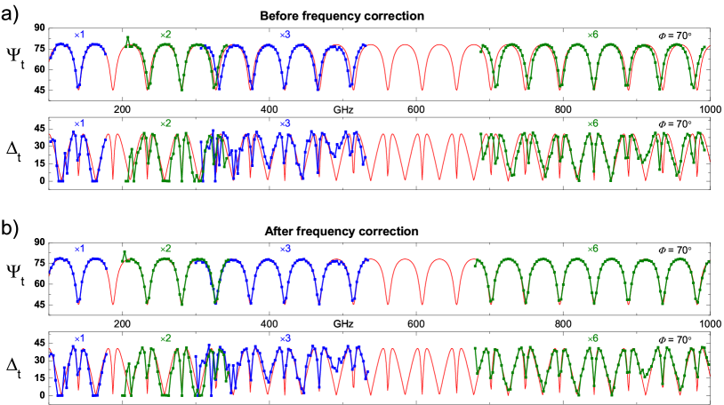
For the THz FDS ellipsometer the frequency of the THz radiation is determined by the high-voltage setting of the BWO cathode potential. The THz frequency vs. BWO cathode voltage function is in first order linear in voltage but requires non-linear voltage correction terms, and hence calibration. An example illustrating an insufficiently frequency calibrated BWO is shown in Fig. 5 a), which depicts experimental (symbols) standard ellipsometry transmission and respective best-match model calculated (lines) , data for a nominally 1 mm thick silicon etalon at angle of incidence . A relatively good match between experiment and model is achieved for all frequency multipliers around a center frequency in each multiplication range, but a growing mismatch is observed towards the upper and lower ends of the respective multiplier range. Further, the magnitude of deviation scales with the frequency multiplication factor. The observed deviations between experiment and calculated data suggest a slight inaccuracy of the voltage-frequency calibration of the BWO ( multiplier) relation provided by the manufacturer.
In order to frequency calibrate the THz FDS ellipsometer we augmented the method used by Naftaly et al. [43] to calibrate the frequency of THz TDS. The idea is to employ Fabry-Pérot etalons with a neglectable absorption and dispersion of the index of refraction in the THz spectral range. Potential materials are, e.g., semi-insulating Si, semi-insulating 4H-SiC or sapphire. [44, 45] We employed high-resistivity, floating-zone silicon because of its optical isotropy. A set of double-side polished Si wafers with a thickness of mm and 1 mm and a diameter of mm, cut out of the same ingot with nominal resistivity cm was used.444For such resistivity values the free-charge careers make negligible contribution to the absorption coefficient and the index of refraction. Additionally, a slab with a thickness of mm was created by stacking three cleaned segments of a 1 mm thick wafer together. Standard ellipsometry parameters and were recorded for all three thicknesses in transmission mode in all frequency ranges (, , and frequency multiplications) at four angles of incidence , , and .
The data was analyzed employing a linear regression algorithm (software: IDL) using an optical model describing the polarization response of an air/Si/air Fabry-Pérot etalon with indexes of refraction and for air and Si ( for both), respectively. The ellipsometric parameters can be written as
| (9) |
where and , and are the respective transmission and reflection Fresnel coefficients for - and -polarized light [1] for the air/etalon interface. The parameter describes the total phase variation between the directly transmitted beam and the next higher transmitted beam, where and are the speed of light and the angular frequency, respectively.
A 4th-order polynomial for calibration of the output frequency vs. voltage of the BWO ( multiplication) was used
| (10) |
Hence, the model parameters are the five coefficients of the frequency correction polynomial, the Si index of refraction and the wafer thicknesses. The thickness parameters of the nominally 0.5 mm and 1 mm thick wafers were determined from standard ellipsometry data recorded in reflection mode with an infrared ellipsometer (IRSE, J.A. Woollam Co., Inc.) at angles of incidence of 50∘, 60∘ and 70∘. This instrument provides ellipsometric data in the range 7.5–240 THz (250–8000 cm-1). The infrared ellipsometry data was analyzed assuming the optical constants of Si and their dispersions as determined in Ref. 46, and we obtained m and m. These parameters were kept constant during the THz frequency calibration procedure. The index of refraction of Si in the THz range was also kept constant at the literature value of [46].
Figure 5b shows best-match model calculated data where the non-linear frequency-voltage correction terms were included into the best-match model parameter base. As can be seen, the Fabry-Pérot oscillations in the and data now match between experimental and model calculated data for the base tube and all frequency multiplication factors investigated here . The coefficients, as defined in Eqn. 10 are GHz, GHz/V1/2, GHz/V, GHz/V3/2 and GHz/V2.
V Applications
V-A Isotropic materials
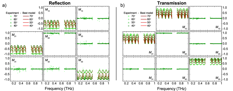
To demonstrate the reflection and transmission Mueller matrix capabilities of the THz FDS ellipsometer to isotropic materials we chose silicon. A high-resistivity, floating-zone silicon wafer different from the one used for the frequency calibration was measured. Figure 6 displays the experimental (green) reflection and transmission Mueller matrix data, recorded at four different angles of incidence , , and , over the full frequency range from 0.1 THz to 1 THz (, , and frequency multiplications), together with corresponding best-match model calculated data (red). Note that the measured elements of the off-diagonal blocks of the Mueller matrix and vanish, as expected for isotropic materials [1]. All data was analyzed simultaneously and the only varied model parameters were the index of refraction, the Si thickness and the offset to the angle of incidence, which is kept constant for all angles of incidence. The excellent agreement between experimental and calculated data further demonstrates that the frequency calibration procedure corrects for the initially observed frequency deviations. The best-match calculated of Si agrees very well (within the error bars) with the value of [46] used in the frequency calibration. This indicates that an accuracy of the index of refraction of one thousandth can typically be achieved with the THz ellipsometer. The best-match calculated values for the Si thickness and the offset in the angle of incidence were determined to be m and , respectively.
V-B Anisotropic materials
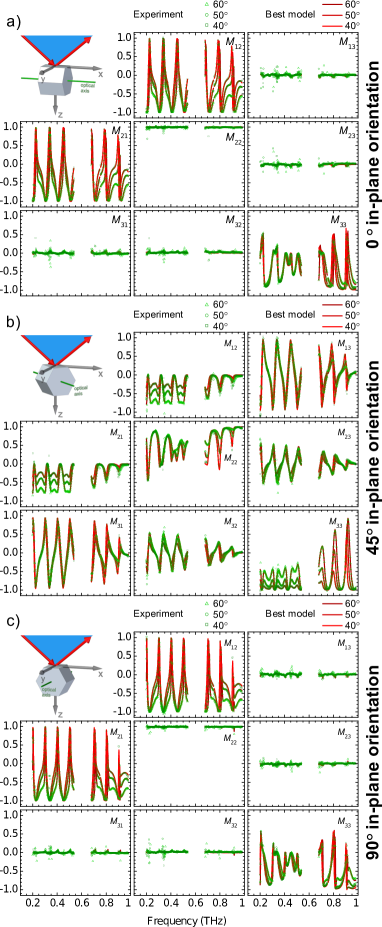
Many technologically relevant materials either in the form of active layers or substrates are optically anisotropic [47]. Examples include wide band gap materials for optoelectronics and high-frequency and power applications such as GaN, Ga2O3, ZnO, CdTe and substrates, such as silicon carbide, quartz and sapphire. Here we demonstrate THz FDS generalized ellipsometry characterization of sapphire as an example. Sapphire is uniaxial with its optical axis along the [0001] direction (c-axis) [48]. Figure 7 displays experimental (green) Mueller matrix data recorded in reflection mode for -Al2O3 (sapphire) with an m-plane (100) surface orientation, together with corresponding best-model calculations (red). Three nominal in-plane orientations , and 555The azimuth angle is the angle between the optical axis (indicated in in the inserts of Fig. 7) and the normal of the plane of incidence. and three angles of incidence , and were measured using the , and frequency multipliers. Note that the measured block off-diagonal Mueller matrix elements (, ) vanish for the high symmetry orientations and . On the other hand for the in-plane orientation mode conversion appears and therefore all Mueller matrix elements reveal spectra different from zero.
The THz data was analyzed together with standard ellipsometry data from a c-plane –Al2O3 sample recorded in the mid-infrared spectral range (IRSE, J.A. Woollam Co., Inc.), using the model described in Ref. 49. During data analysis the -angles of each in-plane orientation and frequency multiplier range were varied independently. All -angels were found to be within of their nominal value. Further, the out-of-plane and the in-plane indices of refraction were varied and determined as and , respectively. These values are in excellent agreement with the refractive indices and determined by far-infrared and THz TDS [44]. The best model parameters for the sapphire thickness and angle of incidence offset were determined to be m and , respectively.
V-C Terahertz optical Hall effect (THz-OHE)
The OHE is a physical effect analogue to the electric Hall effect, which appears at high (optical) frequencies in terms of optical birefringence and is measured using generalized ellipsometry [50]. The OHE allows for detection of three free charge carrier parameters, charge density, charge mobility and effective mass [51, 52, 53, 54, 55]. The magnitude of the OHE birefringence can be further tuned by adding a cavity with varying thickness on the backside of a (transparent) sample [42, 56, 57].
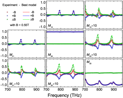
Here we present cavity-enhanced OHE in a high electron mobility transistor (HEMT) structure with a two dimensional electron gas (2DEG) channel as an example. We employ a neodymium permanent magnet with a surface field of T and a fixed cavity of between the sample and the surface of the permanent magnet. The HEMT structure consists of an Al0.75Ga0.25N barrier layer on 2-m-thick GaN layer on a 4H-SiC substrate employing an AlN nucleation layer [58]. Figure 8 shows experimental (symbols) OHE data together with best model calculations (lines) for two opposing magnetic field directions perpendicular to the sample surface, together with the respective difference. A model consisting of air/AlGaN//GaN 2DEG channel//GaN layer/AlN nucleation layer/SiC was used for the best-match model calculations. The model dielectric functions of all constituents included phonon contributions as described in Ref. [50]. Only the 2DEG channel was found to exhibit free charge carriers, which was accounted for in the model dielectric function using the modified Drude model in the presence of magnetic field [50].
The OHE signal from the 2DEG is enhanced by the substrate/air-gap cavity and can be observed in the off diagonal block elements of the Mueller matrix . Note that the symmetry properties of the corresponding off-diagonal elements of the Mueller matrix are fundamentally different for magneto-optic induced birefringence (, also , see Fig. 8), compared to a birefringence induced by structural anisotropy as observed in m-plane sapphire for azimuth angle of (, also , see Fig. 7b). The best-match model parameters from the simultaneous analysis of data from all field directions and the difference data were a sheet carrier density of , effective mass of , and a mobility of for the 2DEG, for the 4H-SiC substrate, and a air gap thickness of . The 2DEG density and mobility parameters are consistent with the respective values typically reported for AlGaN/GaN HEMTs [59, 58]. The 2DEG effective mass parameter is somewhat higher than the bulk GaN electron mass of 0.232 [60], which is in agreement with previous reports [52, 61, 56]. The observed difference could be attributed to a penetration of the 2DEG wavefunction into the AlGaN barrier layer that was shown to be strongly affected by temperature [52] and it is further discussed in Ref. [56].
V-D in-situ THz OHE
The FDS THz ellipsometer can be equipped with a gas cell for in-situ measurements under different ambient conditions (see Fig. 3b). As an example we present here a study of the effects of different, controlled gases and ambient humidity conditions onto the free charge carrier properties of epitaxial graphene.
Graphene, like any other 2D material has an extremely large surface to volume ratio and its properties are therefore highly sensitive to the adjacent media (substrates, liquids, gases) [62, 63, 64, 65, 66, 67]. For a variety of growth methods (epitaxial, exfoliated, CVD grown) ambient doping can be observed [62, 63, 64, 65, 66]. Here we present in-situ FDS THz OHE data from monolayer graphene epitaxially grown on 4H-SiC in an Argon atmosphere. The sample was cyclically exposed to air and N2 with different humidities. The experiment was conducted at a fixed THz frequency ( GHz), at an angle of incidence of , using a neodymium permanent magnet with a surface field of T and a fixed cavity of m between the sample and the surface of the permanent magnet. Figure 9a shows in-situ OHE data with the sample exposed to different gas environments and relative humidities. For the data analysis an optical model consisting of air/graphene/SiC/air-gap/magnet was used. The model dielectric function of the semi-insulating SiC substrates contains only a phonon contribution, while the neodymium magnet is treated as a metal with a Drude dielectric function. Both dielectric functions of SiC and the magnet were determined in separate experiments and included in the data analysis without any changes. The model dielectric function of graphene included contributions from free charge carriers in the presence of magnetic field as detailed in Ref. 57. The effective mass of graphene was coupled to the sheet carrier concentration using from Ref. 68, where and are the Plank constant and the Fermi velocity, respectively. The THz OHE showed that free charge carriers in the epitaxial graphene were electrons. The results on best-match calculated free electron density and mobility parameters of epitaxial graphene are shown in Fig. 9b.
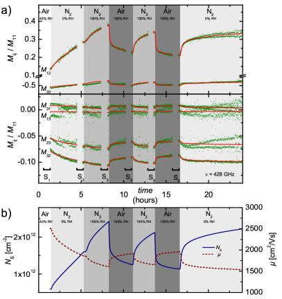
It can be seen that significant changes in the free charge carrier properties occur upon cyclic variation of the environment from air to N2. We have recently reported similar findings for single layer graphene exposed to N2 and He with 0% relative humidity [69]. Here, an increase of the electron density is observed, independent on the relative humidity, when N2 is injected into the gas cell. The process can be reversed to a certain extent, and the carrier density can be reduced by injecting air with 100% humidity. This behavior indicates that the ambient-doping mechanism depends on components in air other than N2, namely O2 or CO2. A possible doping mechanism based on a redox reaction involving H2O, O2 and CO2 is discussed in Ref. 62. While this reaction may not be the only possible chemical process, it is described as the most dominant [70]. The largest variation in from cm-2 to cm-2 is observed in the first two cycles with initial state of graphene being already exposed to ambient conditions for several months. It is worth mentioning that no complete reversal in is observed in the following cycles. These results indicate that the electronic properties of epitaxial graphene may change over the course of several days, if the graphene sample underwent a change of the ambient conditions. This is important to consider if epitaxial graphene is studied, since the results may be changing drastically over time.
The exposure of epitaxial graphene to different gases also results in significant changes in its free electron mobility parameter, (Fig. 9b). The observed variation in mobility can be correlated to the change in free hole density, 1/. This indicates that it is possible that only the carrier density in the graphene changes as a result of gas exposure and where the observed change in mobility is only given by the dependence. However, scattering due to charge impurities could not be excluded. Further details discussing the scattering mechanisms in epitaxial graphene under exposure of different gases can be found in Ref. [69].
VI Conclusion
We have presented the newly designed Terahertz (THz) frequency-domain spectroscopy (FDS) ellipsometer at the Terahertz Material Analysis Center (THeMAC) at Linköping university and have demonstrated its application to a variety of technologically important materials and heterostructures. We have shown that employing concepts used in stealth technology for the instrument geometry and scattering anti-static coating, and modulation of the backward wave oscillator (BWO) THz source allows for effective suppression of standing waves enabling accurate ellipsometry measurements with high spectral resolution (of the order of MHz). We further have demonstrated an etalon-based method for frequency calibration in THz FDS ellipsometry.
The instrument can incorporate various sample compartments, such as a superconducting magnet, in-situ gas cells or resonant sample cavities, for example. Reflection and transmission ellipsometry measurements over a wide range of angles of incidence for isotropic (Si) and anisotropic (sapphire) bulk samples have been presented and used for the determination of the material dielectric constants. We have further demonstrated results from cavity enhanced THz optical Hall effect experiments on an AlGaN/GaN high electron mobility transistor structure (HEMT), determining the free charge carrier density, mobility and effective mass parameters of the 2D electron gas (2DEG) at room temperature. Finally, we have shown through in-situ experiments on epitaxial monolayer graphene exposed to different gases and humidities that THz FDS ellipsometry is capable of determining free charge carrier properties and following their changes upon variation of ambient conditions in atomically thin layers. Therefore, THz FDS ellipsometry has been shown to be an excellent tool for studying free charge carrier and optical properties of thin films, device heterostructures and bulk materials, which are important for current and future electronic applications. Exciting perspectives of applying THz FDS ellipsometry for exploring low-energy excitation phenomena in condensed and soft matter, such as the vibrational, charge and spin transport properties of magnetic nanolaminates, polymers and hybrid structures for photovoltaics and organic electronics; and determination of THz optical constants and signatures of security and metamaterials are envisioned.
Acknowledgment
The authors would like to acknowledge Tino Hofmann (University of North Carolina, Charlotte) for the discussions and input that helped bringing this project forward. Further we would like to thank Craig M. Herzinger (J.A. Woollam Co., Inc.) for support in ellipsometry software development and for numerous fruitful discussions. We thank Jr-Tai Chen (SweGaN AB and Linköping University) for growing and providing the HEMT sample, Jan Šik (On Semiconductor) for providing intrinsic Si wafers, and Rositsa Yakimova (Linköping University and Graphensic AB) for collaboration regarding graphene growth. We acknowledge support from the Swedish Foundation for Strategic Research (SSF, grants No. FFL12-0181, RIF14-055), ÅForsk (grant No. 13-318), the Swedish Research Council (VR Contracts 2013-5580 and 2016-00889), the Swedish Governmental Agency for Innovation Systems (VINNOVA grant No. 2011-03486), the Swedish Government Strategic Research Area in Materials Science on Functional Materials at Linköping University (Faculty Grant SFO Mat LiU No 2009 00971), the National Science Foundation through the Center for Nanohybrid Functional Materials (EPS-1004094), the Nebraska Materials Research Science and Engineering Center (DMR-1420645), and awards CMMI 1337856 and EAR 1521428.
References
- [1] H. Fujiwara, Spectroscopic Ellipsometry. New York: John Wiley & Sons, 2007.
- [2] M. Dressel and G. Grüner, Electrodynamics of Solids, Cambridge University Press, London, 2002.
- [3] M. Schubert, “Polarization-dependent optical parameters of arbitrarily anisotropic homogeneous layered systems,” Phys. Rev. B, vol. 53, pp. 4265–4274, Feb. 1996.
- [4] J. Hlinka, T. Ostapchuk, D. Nuzhnyy, J. Petzelt, P. Kuzel, C. Kadlec, P. Vanek, I. Ponomareva, and L. Bellaiche, “Coexistence of the phonon and relaxation soft modes in the terahertz dielectric response of tetragonal ,” Phys. Rev. Lett., vol. 101, p. 167402, Oct 2008.
- [5] H. Cheon, H.-j. Yang, S.-H. Lee, Y. A. Kim, and J.-H. Son, “Terahertz molecular resonance of cancer dna,” Scientific Reports, vol. 6, p. 37103, Nov 2016, article.
- [6] S. Baierl, M. Hohenleutner, T. Kampfrath, A. K., Zvezdin, A. V., Kimel, R. Huber, and V. R. Mikhaylovskiy, “Nonlinear spin control by terahertz-driven anisotropy fields,” Nat Photon, vol. 10, no. 11, pp. 715–718, Nov 2016, letter.
- [7] Y. Mukai, H. Hirori, T. Yamamoto, H. Kageyama, and K. Tanaka, “Antiferromagnetic resonance excitation by terahertz magnetic field resonantly enhanced with split ring resonator,” Applied Physics Letters, vol. 105, no. 2, p. 022410, 2014.
- [8] M. Sotome, N. Kida, S. Horiuchi, and H. Okamoto, “Visualization of ferroelectric domains in a hydrogen-bonded molecular crystal using emission of terahertz radiation,” Applied Physics Letters, vol. 105, no. 4, p. 041101, 2014.
- [9] T. Hofmann, C. M. Herzinger, C. Krahmer, K. Streubel, and M. Schubert, “The optical hall effect,” Phys. Status Solidi A, vol. 205, no. 4, pp. 779–783, 2008.
- [10] M. C. Hoffmann, K.-L. Yeh, J. Hebling, and K. A. Nelson, “Efficient terahertz generation by optical rectification at 1035 nm,” Opt. Express, vol. 15, no. 18, pp. 11 706–11 713, Sep 2007.
- [11] S. B. Qadri, D. H. Wu, B. D. Graber, N. A. Mahadik, and A. Garzarella, “Failure mechanism of thz gaas photoconductive antenna,” Applied Physics Letters, vol. 101, no. 1, p. 011910, 2012.
- [12] G. Zhao, R. N. Schouten, N. van der Valk, W. T. Wenckebach, and P. C. M. Planken, “Design and performance of a thz emission and detection setup based on a semi-insulating gaas emitter,” Review of Scientific Instruments, vol. 73, no. 4, pp. 1715–1719, 2002.
- [13] B. Globisch, R. J. B. Dietz, T. Göbel, M. Schell, W. Bohmeyer, R. Müller, and A. Steiger, “Absolute terahertz power measurement of a time-domain spectroscopy system,” Opt. Lett., vol. 40, no. 15, pp. 3544–3547, Aug 2015.
- [14] A. Nahata, A. S. Weling, and T. F. Heinz, “A wideband coherent terahertz spectroscopy system using optical rectification and electro-optic sampling,” Applied Physics Letters, vol. 69, no. 16, pp. 2321–2323, 1996.
- [15] J. Takayanagi, S. Kanamori, K. Suizu, M. Yamashita, T. Ouchi, S. Kasai, H. Ohtake, H. Uchida, N. Nishizawa, and K. Kawase, “Generation and detection of broadband coherent terahertz radiation using 17-fs ultrashort pulse fiber laser,” Opt. Express, vol. 16, no. 17, pp. 12 859–12 865, Aug 2008.
- [16] A. Tomasino, A. Parisi, S. Stivala, P. Livreri, A. C. Cino, A. C. Busacca, M. Peccianti, and R. Morandotti, “Wideband THz time domain spectroscopy based on optical rectification and electro-optic sampling,” Scientific Reports, vol. 3, no. 1, oct 2013.
- [17] Y. Zhou, Y. E, L. Zhu, M. Qi, X. Xu, J. Bai, Z. Ren, and L. Wang, “Terahertz wave reflection impedance matching properties of graphene layers at oblique incidence,” Carbon, vol. 96, pp. 1129 – 1137, 2016.
- [18] W. Aenchbacher, M. Naftaly, and R. Dudley, “Line strengths and self-broadening of pure rotational lines of carbon monoxide measured by terahertz time-domain spectroscopy,” Appl. Opt., vol. 49, no. 13, pp. 2490–2496, May 2010.
- [19] W. Withayachumnankul and M. Naftaly, “Fundamentals of measurement in terahertz time-domain spectroscopy,” Journal of Infrared, Millimeter, and Terahertz Waves, vol. 35, no. 8, pp. 610–637, Aug 2014.
- [20] P. U. Jepsen and B. M. Fischer, “Dynamic range in terahertz time-domain transmission and reflection spectroscopy,” Opt. Lett., vol. 30, no. 1, pp. 29–31, Jan 2005.
- [21] D. Jahn, S. Lippert, M. Bisi, L. Oberto, J. C. Balzer, and M. Koch, “On the influence of delay line uncertainty in thz time-domain spectroscopy,” Journal of Infrared, Millimeter, and Terahertz Waves, vol. 37, no. 6, pp. 605–613, Jun 2016.
- [22] T. Nagashima and M. Hangyo, “Measurement of complex optical constants of a highly doped si wafer using terahertz ellipsometry,” Applied Physics Letters, vol. 79, no. 24, pp. 3917–3919, 2001.
- [23] N. Matsumoto, T. Fujii, K. Kageyama, H. Takagi, T. Nagashima, and M. Hangyo, “Measurement of the soft-mode dispersion in srtio3 by terahertz time-domain spectroscopic ellipsometry,” Jpn. J. Appl. Phys., vol. 48, no. 9, p. 09KC11, 2009.
- [24] M. Neshat and N. P. Armitage, “Terahertz time-domain spectroscopic ellipsometry: instrumentation and calibration,” Opt. Express, vol. 20, no. 27, pp. 29 063–29 075, Dec 2012.
- [25] P. Marsik, K. Sen, J. Khmaladze, M. Yazdi-Rizi, B. P. P. Mallett, and C. Bernhard, “Terahertz ellipsometry study of the soft mode behavior in ultrathin srtio3 films,” Applied Physics Letters, vol. 108, no. 5, p. 052901, 2016.
- [26] M. Yamashita, H. Takahashi, T. Ouchi, and C. Otani, “Ultra-broadband terahertz time-domain ellipsometric spectroscopy utilizing gap and gase emitters and an epitaxial layer transferred photoconductive detector,” Applied Physics Letters, vol. 104, no. 5, p. 051103, 2014.
- [27] I. A. Azarov, V. A. Shvets, V. Y. Prokopiev, S. A. Dulin, S. V. Rykhlitskii, Y. Y. Choporova, B. A. Knyazev, V. N. Kruchinin, and M. V. Kruchinina, “A terahertz ellipsometer,” Instruments and Experimental Techniques, vol. 58, no. 3, pp. 381–388, May 2015.
- [28] A. A. Galuza, V. K. Kiseliov, I. V. Kolenov, A. I. Belyaeva, and Y. M. Kuleshov, “Developments in thz-range ellipsometry: Quasi-optical ellipsometer,” IEEE Transactions on Terahertz Science and Technology, vol. 6, no. 2, pp. 183–190, March 2016.
- [29] T. Hofmann, C. M. Herzinger, U. Schade, M. Mross, J. A. Woollam, and M. Schubert, “Terahertz ellipsometry using electron-beam based sources,” MRS Proceedings, vol. 1108, 2008.
- [30] W. Kleen, Electronics of Microwave Tubes. Elsevier Science, 2012.
- [31] K. Button, Infrared and Millimeter Waves, ser. Infrared and millimeter waves. Elsevier Science, 2012, no. Bd. 1.
- [32] N. Wiener, “Generalized harmonic analysis,” Acta Mathematica, vol. 55, no. 0, pp. 117–258, 1930.
- [33] A. Khintchine, “Korrelationstheorie der stationären stochastischen prozesse,” Mathematische Annalen, vol. 109, no. 1, pp. 604–615, Dec 1934.
- [34] C. J. Dainty, A. E. Ennos, M. Fran on, J. W. Goodman, T. S. McKechnie, and G. Parry, Laser Speckle and Related Phenomena. Springer Berlin Heidelberg, 1975.
- [35] R. C. JONES, “A new calculus for the treatment of optical systems,” J. Opt. Soc. Am., vol. 31, no. 7, pp. 488–493, Jul 1941.
- [36] E. Hecht, Optics. Reading MA: Addison-Wesley, 1987.
- [37] M. Schubert, Infrared Ellipsometry on semiconductor layer structures: Phonons, plasmons and polaritons, ser. Springer Tracts in Modern Physics. Berlin: Springer, 2004, vol. 209.
- [38] M. Schubert, B. Rheinländer, J. A. Woollam, B. Johs, and C. M. Herzinger, “Extension of rotating-analyzer ellipsometry to generalized ellipsometry: determination of the dielectric function tensor from uniaxial tio2,” J. Opt. Soc. Am. A, vol. 13, no. 4, pp. 875–883, Apr. 1996.
- [39] D. Goldstein and D. Goldstein, Polarized Light, Revised and Expanded, ser. Optical Engineering - Marcel Dekker. Taylor & Francis, 2011.
- [40] G. E. Jellison, “Spectroscopic ellipsometry data analysis: measured versus calculated quantities,” Thin Solid Films, vol. 313-314, no. 0, pp. 33–39, 1998.
- [41] C. M. Herzinger, S. E. Green, and B. D. Johs, “Odd bounce image rotation system in ellipsometer systems,” U.S.A. Patent U.S. Patent No. 6,795,184, Sep. 21, 21 September 2004.
- [42] S. Knight, S. Schöche, V. Darakchieva, P. Kühne, J.-F. Carlin, N. Grandjean, C. M. Herzinger, M. Schubert, and T. Hofmann, “Cavity-enhanced optical hall effect in two-dimensional free charge carrier gases detected at terahertz frequencies,” Optics Letters, vol. 40, no. 12, p. 2688, jun 2015.
- [43] M. Naftaly, R. A. Dudley, and J. R. Fletcher, “An etalon-based method for frequency calibration of terahertz time-domain spectrometers (thz tds),” Optics Communications, vol. 283, pp. 1849–1853, may 2010.
- [44] D. R. Grischkowsky, S. R. Keiding, M. P. van Exter, and C. Fattinger, “Far-infrared time-domain spectroscopy with terahertz beams of dielectrics and semiconductors,” Journal of the Optical Society of America B Optical Physics, vol. 7, pp. 2006–2015, oct 1990.
- [45] M. Naftaly, J. F. Molloy, B. Magnusson, Y. M. Andreev, and G. V. Lanskii, “Silicon carbide—a high-transparency nonlinear material for thz applications,” Optics Express, vol. 24, p. 2590, feb 2016.
- [46] D. Y. Smith, W. Karstens, E. Shiles, and M. Inokuti, “Defect and analysis effects in the infrared optical properties of silicon,” Physica Status Solidi B Basic Research, vol. 250, pp. 271–277, feb 2013.
- [47] K. Gurnett and T. Adams, “Native substrates for gan: the plot thickens,” III-Vs Review, vol. 19, no. 9, pp. 39 – 41, 2006.
- [48] W. E. Lee and K. P. D. Lagerlof, “Structural and electron diffraction data for sapphire (-al2o3),” Journal of Electron Microscopy Technique, vol. 2, no. 3, pp. 247–258, 1985.
- [49] M. Schubert, T. E. Tiwald, and C. M. Herzinger, “Infrared dielectric anisotropy and phonon modes of sapphire,” Phys. Rev. B, vol. 61, no. 12, pp. 8187–, Mar. 2000.
- [50] M. Schubert, P. Kühne, V. Darakchieva, and T. Hofmann, “Optical hall effect—model description: tutorial,” J. Opt. Soc. Am. A, vol. 33, no. 8, pp. 1553–1568, Aug 2016.
- [51] P. Kühne, T. Hofmann, C. Herzinger, and M. Schubert, “Terahertz optical-hall effect for multiple valley band materials: n-type silicon,” Thin Solid Films, vol. 519, no. 9, pp. 2613 – 2616, 2011, 5th International Conference on Spectroscopic Ellipsometry (ICSE-V).
- [52] T. Hofmann, P. Kühne, S. Schöche, J.-T. Chen, U. Forsberg, E. Janzén, N. B. Sedrine, C. M. Herzinger, J. A. Woollam, M. Schubert, and V. Darakchieva, “Temperature dependent effective mass in AlGaN/GaN high electron mobility transistor structures,” Appl. Phys. Lett., vol. 101, no. 19, p. 192102, 2012.
- [53] S. Schöche, P. Kühne, T. Hofmann, M. Schubert, D. Nilsson, A. Kakanakova-Georgieva, E. Janzén, and V. Darakchieva, “Electron effective mass in al0.72ga0.28n alloys determined by mid-infrared optical hall effect,” Appl. Phys. Lett., vol. 103, no. 21, pp. –, 2013.
- [54] S. Schöche, T. Hofmann, V. Darakchieva, N. B. Sedrine, X. Wang, A. Yoshikawa, and M. Schubert, “Infrared to vacuum-ultraviolet ellipsometry and optical hall-effect study of free-charge carrier parameters in mg-doped inn,” J. Appl. Phys., vol. 113, no. 1, p. 013502, 2013.
- [55] S. Schöche, T. Hofmann, D. Nilsson, A. Kakanakova-Georgieva, E. Janz n, P. Kühne, K. Lorenz, M. Schubert, and V. Darakchieva, “Infrared dielectric functions, phonon modes, and free-charge carrier properties of high-al-content alxga1-xn alloys determined by mid infrared spectroscopic ellipsometry and optical hall effect,” Journal of Applied Physics, vol. 121, no. 20, p. 205701, 2017.
- [56] N. Armakavicius, J.-T. Chen, T. Hofmann, S. Knight, P. Kühne, D. Nilsson, U. Forsberg, E. Janz n, and V. Darakchieva, “Properties of two-dimensional electron gas in algan/gan hemt structures determined by cavity-enhanced thz optical hall effect,” physica status solidi (c), vol. 13, no. 5-6, pp. 369–373, 2016.
- [57] N. Armakavicius, C. Bouhafs, V. Stanishev, P. Kühne, R. Yakimova, S. Knight, T. Hofmann, M. Schubert, and V. Darakchieva, “Cavity-enhanced optical hall effect in epitaxial graphene detected at terahertz frequencies,” Applied Surface Science, vol. 421, no. Part B, pp. 357 – 360, 2017, 7th International Conference on Spectroscopic Ellipsometry.
- [58] J.-T. Chen, I. Persson, D. Nilsson, C.-W. Hsu, J. Palisaitis, U. Forsberg, P. O. Å. Persson, and E. Janzén, “Room-temperature mobility above 2200 cm2/vs of two-dimensional electron gas in a sharp-interface algan/gan heterostructure,” Applied Physics Letters, vol. 106, no. 25, p. 251601, 2015.
- [59] V. M. Polyakov, V. Cimalla, V. Lebedev, K. Köhler, S. Müller, P. Waltereit, and O. Ambacher, “Impact of al content on transport properties of two-dimensional electron gas in gan/alxga1-xn/gan heterostructures,” Appl. Phys. Lett., vol. 97, no. 14, p. 142112, 2010.
- [60] A. Kasic, M. Schubert, S. Einfeldt, D. Hommel, and T. E. Tiwald, “Free-carrier and phonon properties of n- and p-type hexagonal GaN films measured by infrared ellipsometry,” Phys. Rev. B, vol. 62, no. 11, pp. 7365–7377, Sep. 2000.
- [61] B. F. Spencer, W. F. Smith, M. T. Hibberd, P. Dawson, M. Beck, A. Bartels, I. Guiney, C. J. Humphreys, and D. M. Graham, “Terahertz cyclotron resonance spectroscopy of an algan/gan heterostructure using a high-field pulsed magnet and an asynchronous optical sampling technique,” Appl. Phys. Lett., vol. 108, no. 21, p. 212101, 2016.
- [62] A. N. Sidorov, K. Gaskill, M. B. Nardelli, J. L. Tedesco, R. L. Myers-Ward, C. R. E. Jr., T. Jayasekera, K. W. Kim, R. Jayasingha, A. Sherehiy, R. Stallard, and G. U. Sumanasekera, “Charge transfer equilibria in ambient-exposed epitaxial graphene on 6h-sic,” J. Appl. Phys., vol. 111, p. 113706, 2012.
- [63] C. E. Giusca, V. Panchal, M. Munz, V. D. Wheeler, L. O. Nyakiti, R. L. Myers-Ward, D. K. Gaskill, and O. Kazakova, “Water affinity to epitaxial graphene: the impact of layer thickness,” Adv. Mater. Interf., vol. 2, no. 16, p. 1500252, 2015.
- [64] M. W. Nomani, R. Shishir, M. Qazi, D. Diwan, V. Shields, M. Spencer, G. S. Tompa, N. M. Sbrockey, and G. Koley, “Highly sensitive and selective detection of no using epitaxial graphene on 6h-sic,” Sens. Actuators B Chem., vol. 150, no. 1, pp. 301–307, 2010.
- [65] Y. Yang and R. Murali, “Binding mechanisms of molecular oxygen and moisture to graphene,” Appl. Phys. Lett., vol. 98, no. 9, p. 093116, 2011.
- [66] J. Chan, A. Venugopal, A. Pirkle, S. McDonnell, D. Hinojos, C. W. Magnuson, R. S. Ruoff, L. Colombo, R. M. Wallace, and E. M. Vogel, “Reducing extrinsic performance-limiting factors in graphene grown by chemical vapor deposition,” ACS Nano, vol. 6, no. 4, pp. 3224–3229, 2012.
- [67] C. J. Docherty, C.-T. Lin, H. J. Joyce, R. J. Nicholas, L. M. Herz, L.-J. Li, and M. B. Johnston, “Extreme sensitivity of graphene photoconductivity to environmental gases,” Nat. Commun., vol. 3, p. 1228, 2012.
- [68] K. S. Novoselov, A. K. Geim, S. V. Morozov, D. Jiang, M. I. Katsnelson, I. V. Grigorieva, S. V. Dubonos, and A. A. Firsov, “Two-dimensional gas of massless dirac fermions in graphene,” Nature, vol. 438, no. 7065, pp. 197–200, Nov. 2005.
- [69] S. Knight, T. Hofmann, C. Bouhafs, N. Armakavicius, P. Kühne, V. Stanishev, I. G. Ivanov, R. Yakimova, S. Wimer, M. Schubert, and V. Darakchieva, “In-situ terahertz optical hall effect measurements of ambient effects on free charge carrier properties of epitaxial graphene,” Scientific Reports, vol. 7, no. 1, jul 2017.
- [70] V. Chakrapani, J. C. Angus, A. B. Anderson, S. D. Wolter, B. R. Stoner, and G. U. Sumanasekera, “Charge transfer equilibria between diamond and an aqueous oxygen electrochemical redox couple,” Science, vol. 318, p. 1424, 2007.
![[Uncaptioned image]](/html/1712.05283/assets/x10.png) |
Philipp Kühne received in 2009 the Dipl.-Phys. degree from the University of Leipzig, Leipzig, Germany. In 2014 he received a Ph.D. degrees in electrical engineering from the University of Nebraska, Lincoln, USA. Since 2014 he works as a post-doctoral researcher and research engineer at the Terahertz Materials Analysis Center (TeMAC) at the Linköping University, Linköping, Sweden. His work is focused on material analysis with emphasis on ellipsometry. |
![[Uncaptioned image]](/html/1712.05283/assets/x11.png) |
Vallery Stanishev received a M.S. degree in astrophysics from Sofia University, Bulgaria and a Ph.D. degree in astrophysics from Institute of Astronomy, Bulgarian Academy of Sciences, in 1995 and 2002, respectively. He works as a research engineer and and university lecturer at the Linköping University, Linköping, Sweden. His research interests include materials analysis with spectroscopic ellipsometry. |
![[Uncaptioned image]](/html/1712.05283/assets/x12.png) |
Nerijus Armakavicius received B.S. and M.S. degrees in Applied Physics from Kaunas University of Technology, Lithuania, in 2012 and 2014, respectively. Since 2014 he works as a PhD student at the Terahertz Materials Analysis Center at the Linköping University in Sweden. His research interests are spectroscopic ellipsometry, optical Hall effect, two-dimensional electronic materials and advanced semiconductors. |
![[Uncaptioned image]](/html/1712.05283/assets/x13.png) |
Mathias Schubert received Dipl.-Phys., Dr. rer. nat., and Dr. habil. (Physics) degrees from the University of Leipzig, Leipzig, Germany, in 1994, 1997, and 2003, respectively. He received a Dr. tech. h.c. from Linköping University, Sweden, in 2015. He became associate professor and full professor at the University of Nebraska, Lincoln, USA, in 2005 and 2012, respectively. He currently holds the J.A. Woollam Distinguished Professorship Chair. His research interests cover ellipsometry spectroscopy and imaging, the optical Hall effect, advanced semiconductors and functional materials, nanocomposites, optoelectronic devices, conductive organics, in-situ monitoring, and low-symmetry materials. He is also an Associate Editor of Applied Physics Letters. |
![[Uncaptioned image]](/html/1712.05283/assets/x14.png) |
Vanya Darakchieva received a Ph.D. degree in materials science and habilitation in semiconductor materials from the Linköping University, Linköping, Sweden in 2004 and 2009, respectively. She became an associate professor at Linköping University, Linköping, Sweden in 2012. She is head of the Terahertz Materials Analysis Center, and director of the Competence Center for III-Nitride Technology at Linköping University. Her research is focused on novel semiconductor and nanoscale materials for high-frequency and power electronics, and advanced spectroscopic metrology of transport and electronic properties of materials. |