Observation of Inter-layer Excitons in MoSe2 Single Crystals
Abstract
Interlayer excitons are observed coexisting with intralayer excitons in bi-layer, few-layer, and bulk MoSe2 single crystals by confocal reflection contrast spectroscopy. Quantitative analysis using the Dirac-Bloch-Equations provides unambiguous state assignment of all the measured resonances. The interlayer excitons in bilayer MoSe2 have a large binding energy of meV, narrow linewidth of meV, and their spectral weight is comparable to the commonly studied higher-order intralayer excitons. At the same time, the interlayer excitons are characterized by distinct transition energies and permanent dipole moments providing a promising high temperature and optically accessible platform for dipolar exciton physics.
The basic understanding of spatially direct semiconductor excitons dates back to the 1930s Frenkel (1931); Wannier (1937), where an exciton in a single crystal has been described as a Coulomb bound pair of an electron and a hole that spatially overlap in the absence of external electrical or magnetic fields. To create spatially indirect excitons, heterostructures were used, first with coupled GaAs quantum wells Colocci et al. (1990); Butov et al. (1994) and more recently with stacked van der Waals crystal systems (vdWcs) Geim and Grigorieva (2013); Jariwala et al. (2016); Rivera et al. (2015); Philipp Nagler et al. (2017); Zhu et al. (2015); Schaibley et al. (2016); Ross et al. (2017).
Here, we use confocal reflection contrast spectroscopy to show that stable, indirect exciton resonances exist in multilayer single crystals of MoSe2. In these interlayer excitons, the electron and hole are confined to neighboring molecular layers and the associated optical resonances are shown to co-exist with those of the usual intralayer excitons. Mono-, bi-, tri- and few-layer up to bulk crystals on the same substrate are studied systematically and bilayer results are presented with and without encapsulation.
The experimental spectra are analyzed by numerically solving the coupled microscopic gap and Dirac-Bloch equations Meckbach et al. (2017a, b). For all structures, the agreement between the theory and experiment is fully quantitative and allows for an unambiguous state assignment.
The identification of interlayer excitons enriches our basic understanding of the optical and electrical properties of van der Waals crystals. Furthermore, these interlayer excitons promise a new platform for non-equilibrium many-body physics. Similar to indirect excitons in heterostructures, they have a permanent, aligned dipole moment that leads to long-range dipole-dipole interactions and a wide range of associated quantum many-body phenomena Fogler et al. (2014); E.V. Calman ; Mathieu Alloing et al. (2014); Monique Combescot et al. (2017); Su and MacDonald (2017); Berman and Kezerashvili (2017).
Due to their permanent dipole moment, indirect excitons in conventional semiconductor heterostructures are sensitive to local electronic disorders including those at the internal interfaces of the heterostructures. They also have a greatly reduced binding energy and optical transition rate, limiting their operation temperatures and experimental accessibility. In contrast, interlayer excitons in monocrystalline vdWCs do not experience internal interfaces. Furthermore, the external crystal surfaces can be very effectively passivated by hexagonal-boron-nitride (hBN) layers. These near ideal structural conditions reflect themselves in the measured narrow linewidth of 19 meV, which is comparable to that of intra-layer excitons and many times narrower than indirect excitons in vdWc heterostructures. Moreover, due to the close proximity of the neighboring molecular layers, the interlayer excitons maintain a relatively large exciton binding energy, 153 meV in MoSe2. Therefore, they may allow dipolar exciton studies at the presence of relatively high doping densities and temperatures. The interlayer excitons also remain optically active, which will enable convenient optical access to the system and potentially powerful cavity effects Deng et al. (2010); Carusotto and Ciuti (2013). While it will also result in a relatively fast radiative decay and restricts the system to non-equilibrium regime, quantum many-body phenomena have been shown to survive in non-equilibrium systems. Lastly, bi-layer and few-layer vdWcs are easier to fabricate than heterostructures and do not suffer from lattice mismatch or angle rotation between the constituting lattices.
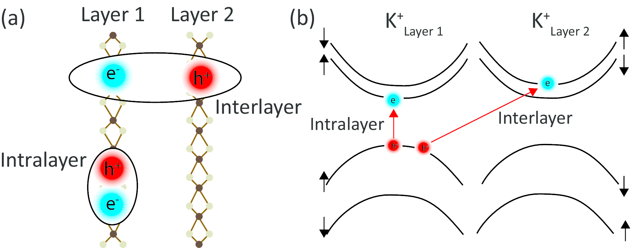

In Fig. 1(a), we schematically show the real-space configuration of the interlayer exciton in a MoSe2 bilayer. Even though the transition from a direct to indirect gap in most vdWc multilayer structures already occurs for the bilayer, the direct gap at the -points of the Brillioun zone is preserved even in the bulk limit, with a dispersion that is flat along the directionYe et al. (2015). This flat dispersion indicates that even in a multilayer structure, the near -point quasi-particles can be considered as effectively two-dimensional, and are strongly confined within individual layers, with the potential to build bound interlayer excitons even in multilayer structures consisting of identical monolayers.
In Fig. 1(b), we show the band and spin configuration for the non-interacting band structure around the -point in an A-B stacked MoSe2 bilayer. Whereas the -points of a monolayer are nonequivalent and related by the parity transformation, they are equivalent in an inversion symmetric bilayer. At each -point, the non-interacting bandstructure is composed of the spin-split valence and conduction bands of layer 1 and a mirror identical copy with reversed spin ordering of layer 2Xu et al. (2014). Consequently, dipole allowed intralayer excitons corresponding to the A-series in MoSe2 are formed by an electron in the lowest conduction band and a hole in the highest valence band, whereas the correspondent interlayer exciton uses the upper spin-split conduction band (see arrows in Fig. 1(b)). Thus, the optical selection rules for the interlayer excitons exhibit similar symmetry properties as those for the intra-layer excitons with the difference that the spin-valley selectivity in a monolayer is replaced by spin-layer selectivity for the excitation with circular polarized light.
To experimentally identify interlayer excitons in vdWc multilayers, we perform confocal reflection spectroscopy with a tungsten lamp light source at 5 K to study the bound electron-hole pairs on MoSe2 flakes with a spatial resolution of m. Signals from the sample were normalized against a point on nearby substrate to produce reflection contrast. Fig. 2(a) shows an optical microscope image of sample A, consisting of an hBN-encapsulated monolayer and bilayer MoSe2. The measured reflection contrast spectrum () for the monolayer region on this sample is shown as black curve in Fig. 2(b), where and are reflection spectrum taken from sample and substrate area, respectively. A typical spectrum of monolayer MoSe2 was observed with reflection peaks corresponding to ( meV) and ( meV) excitons. Due to the sharp linewidth resulting from the hBN encapsulation, we can also identify the excited excitons at meV and at meV, both with much smaller oscillator strengths relative to the states. Because of the rapid decrease of spectral weight with increasing quantum number and interference between different species of excitons, we cannot resolve the excitons states experimentally.
The corresponding optical spectrum in the encapsulated bilayer region is shown in Fig. 2(c). The bilayer spectrum has somewhat broader and resonances and we note a red shift of the dominant resonance of meV and a small blue shift of the resonance of meV, respectively. Strikingly, we also observe two additional peaks above the transition at meV and meV with similar oscillator strength, and a weak spectral feature at meV. Naively, one could try to assign the two peaks above the resonance to the and exciton resonances that are red shifted by the presence of the second layer. However, this assignment is unreasonable due to the similar oscillator strength of the two observed peaks.
To understand the physical origin of the observed features, we employ the theoretical framework that combines an electrostatic model for the Coulomb interaction potential in an anisotropic medium, i.e. the gap equations to determine the interacting gap, and the Dirac-Bloch-Equations (DBE) to compute the linear optical responseMeckbach et al. (2017a). Within this model, the electronic and optical properties around the K-points of the multilayer structures are treated by considering the symmetry induced spin locking of the individual layers and the inter- and intralayer Coulomb interaction. Treating the Hamiltonian of the isolated monolayer within an effective four-band modelXiao et al. (2012), screening of the bands under consideration is included dynamically, whereas screening of all remaining bands and the dielectric environment is contained in the Coulomb matrix element. The material parameters used are listed in Ref. not . This model is based on the observation that the direct gap at the K-points, which contributes dominantly to the optical absorption, is preserved while increasing the number of layers from a monolayer to bulk Ye et al. (2015). At the K points, the out-of-plane effective masses of the valence and conduction bands are typically much larger than those in the in-plane directions. Consequently, the out-of-plane component of the kinetic energy can be neglected and the quasi-particles at the K-points can be considered as quasi-two dimensional, well confined within the layers. These assumptions are strongly supported by recent ARPES measurements, which have revealed the two-dimensional nature of the bands at the K point of the Brillouin zone Riley et al. (2014)
The theory predicts the resonance positions meV and meV at zero density and temperature respectively, which shift to meV and meV in the presence of a small carrier density of . The computed optical spectrum for the encapsulated monolayer is plotted in Fig. 2(b) for comparison with the experiment. In the numerical evaluations, we introduced a phenomenological linewidth with full-width-at-half-maximum(FWHM) of 4 meV for the , 30 meV for other A-exciton resonances and 40 meV for the B-series. The calculation agrees well with the experimentally observed peaks in energy as well as oscillator strengths, allowing for an unambiguous state assignment of the monolayer excitons.
Next, we apply the combined gap and DBE equations to compute the linear optical response for bilayer MoSe2, using the same DFT parameters for the noninteracting band structure as for the monolayer. As long as one considers only the intralayer contributions, the Elliot formulaHaug and Koch (2009) for an arbitrary layer within the multilayer structure is formally identical to that of a monolayer. However, quantitatively, the intralayer contributions are modified via their dependence on the detailed Coulomb matrix elements which are modified by both, the presence of the substrate and the other layers. As a result, each layer in a multilayer configuration experiences a different dielectric environment, generally leading to an intrinsic inhomogeneous broadening of the resonances due to the slightly different contributions from the individual layers. However, for an inversion symmetric bilayer, e.g. a suspended or encapsulated system, both layers are equivalent and resonances corresponding to different intralayer excitons should be degenerate, and thus, do not give rise to additional resonances. For the encapsulated bilayer configuration at zero temperature and carrier density, we theoretically find the lowest -type intra-layer resonances at meV, meV, and meV, with a relative oscillator strength of respectively. Whereas the shift of the exciton resonance agrees with the experimental observations within an accuracy of 10%, the resonance positions and oscillator strengths of the and intralayer states do not match the experimental data, showing that these states are not responsible for the experimentally observed features.
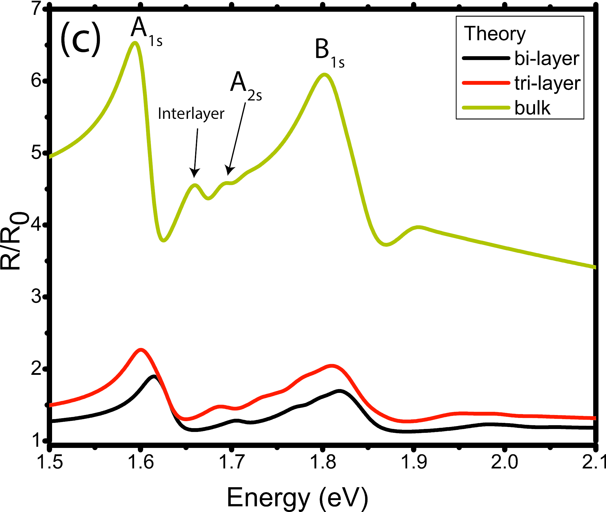
In addition to the intralayer interactions, the theory predicts that the Coulomb attraction between electrons and holes in adjacent layers should give rise to additional bound interlayer excitons. For the encapsulated bilayer configuration, we find a binding energy of meV for the interlayer exciton, only 27% less than the binding energy of meV for the lowest intralayer exciton. As the interlayer exciton uses conduction-band states from the opposite K-valley, introducing a spin splitting of the conduction band leads to a blue shift of the A-interlayer exciton, and a simultaneous red shift of the B-intralayer exciton. Using a meV spin splitting of the conduction band, we find the lowest inter-layer exciton at meV, between the and resonances of the intralayer exciton. To determine the relative oscillator strength, we estimate the dipole matrix element for the inter-layer transition from the -type Mo-orbital centered around the central positions of the adjacent layers, giving . The resulting simulated spectrum for the encapsulated bilayer is shown in Fig. 2(c). The calculations have been performed assuming a nm hBN capping, and we included a phenomenological broadening(FWHM) of meV and meV for A- and B- series, respectively. The results show excellent agreement with the experimentally observed spectra. With the quantitative agreement between theory and experiment, we assign the meV and meV peaks as exciton and A-interlayer exciton, respectively.
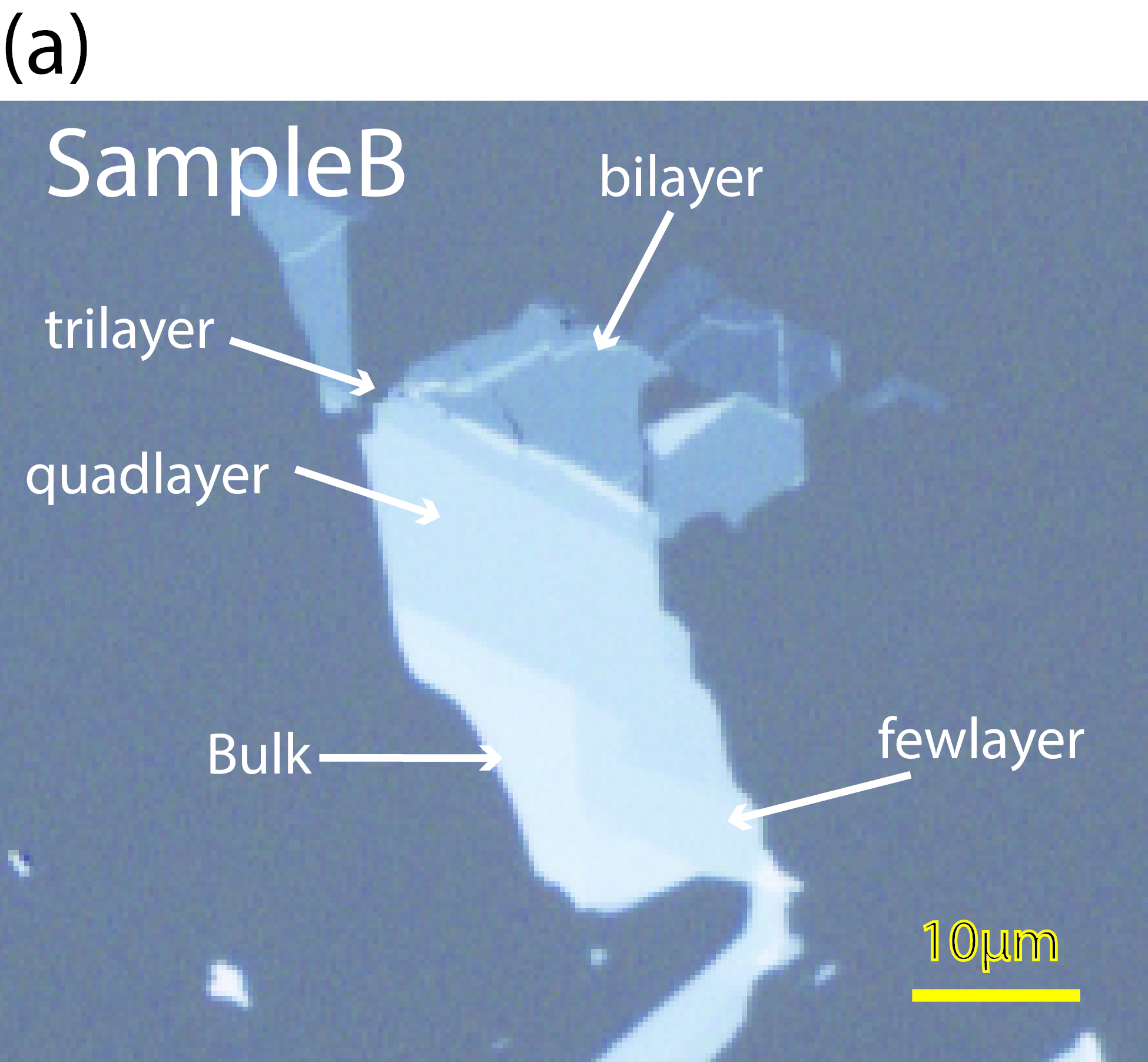
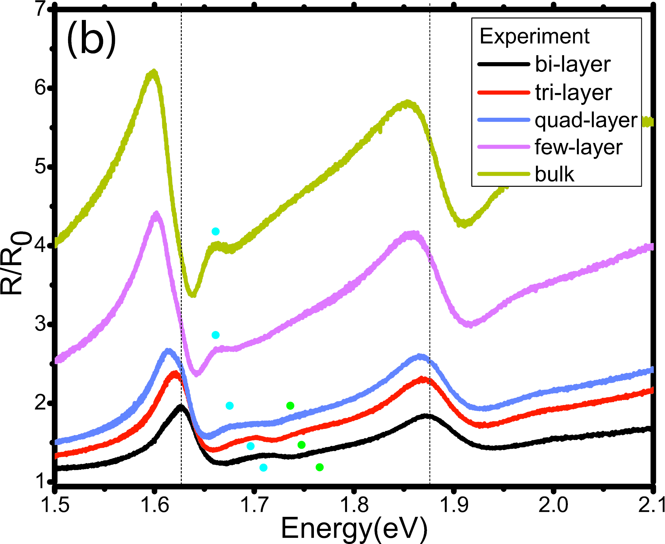
To further support our interpretation based on interlayer exciton states, we study the influence of thickness on the resonance position and oscillator strength in MoSe2 multilayer systems. We prepare sample B (optical microscope image in Fig. 3(a), consisting of MoSe2 monolayer, bilayer, tri-layer, quad-layer and multilayers on a sapphire substrate. In Fig. 3(b), we show the measured reflection contrast for various sample thicknesses. The two main transitions around meV and meV correspond to the and excitons, respectively. Aside from these two features, we also observed the interlayer peak ( meV, blue dot) and shoulder ( meV, green dot) in the bilayer spectrum. As the layer number increases, both intralayer exciton and interlayer exciton should show a redshift behavior due to increasing dielectric screening. Experimentally, the bulk intralayer species and redshift about meV and meV, respectively, from bilayer samples, whereas the observed A-interlayer shows a rather strong redshift of meV as approaching to the bulk limit. Similar to the monolayer, the shifts result from a simultaneously redshift of the interacting gap and exciton binding energy. As can be recognized, the interlayer exciton also becomes more apparent in the bulk limit. Apart from the narrower linewidth ( meV in bilayer and meV in bulk), which is expected due to reducing inhomogeneous broadening arising from the from MoSe2 surfaces, the reason for this is the relative oscillator strength. Whereas intralayer contributions increase linearly with the number of layers, the number of next neighbours and therewith the interlayer contributions increase as , thus doubling the relative oscillator strength going from bilayer to bulk.
We also perform DBE calculations to predict the linear optical response for numbers of layers. Again, we use the same monolayer DFT parameters including the same wavefunction overlap between adjacent layers. The computed optical spectra are plotted in Fig. 3(c). For the A-exciton series, we find good agreement with the experimental data in terms of both exciton resonance energies and oscillator strengths. In particular, we observe the increasing oscillator strength of the interlayer exciton compared to the intralayer exciton. Whereas the shifts of the B-excitons with increasing layer thickness is predicted very accurately, the theoretical results for the multilayers show a systematic red shift of the B-exciton series as compared with experiment, which is not apparent for the monolayer. This systematic discrepancy indicates that interlayer interactions might change the DFT bandstructure going from mono- to bilayer, which is not captured by our model system. Despite this shortcoming, the qualitative and quantitative agreement between theory and experiment provides strong evidence to assign the second peak to the interlayer exciton.
We note that in the ref. Chernikov et al. (2014), the second-lowest feature in WS2 reflection spectra was assigned to the exciton. According to our simulation and experiment, the correct assignment should be A-interlayer exciton.
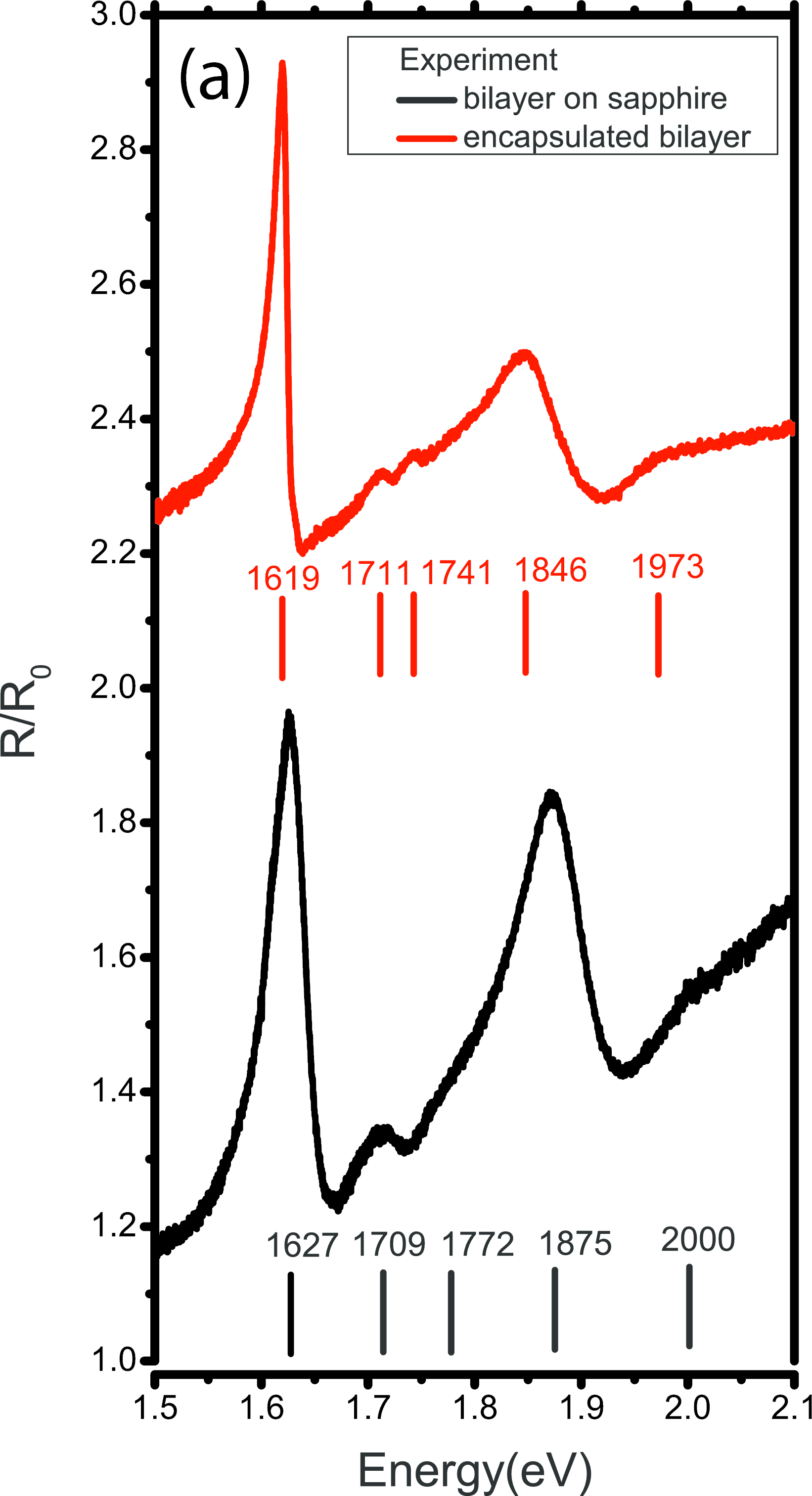
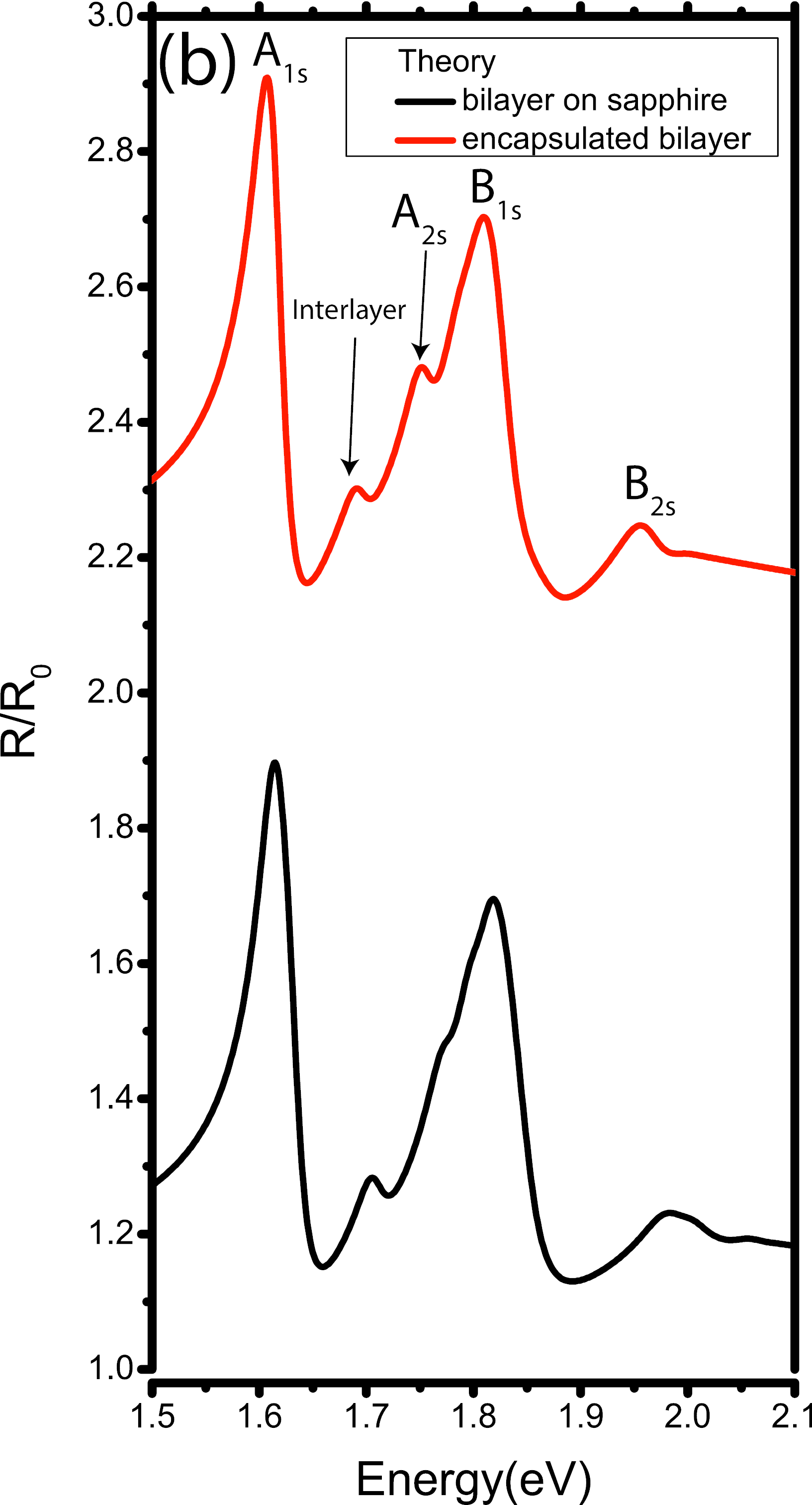
At last, we compare the measured spectra of bilayer MoSe2 with and without hBN encapsulation (Fig. 4(a)). The encapsulated sample is from sample A (bilayer in Fig.2(a)) and the non-encapsulated sample is from sample B (bilayer in Fig. 3(a)). The computed spectra for the above sample structures are also plotted in Fig. 4(b) to show that our model well accounts for the excitonic shift in different screening environments. A direct observation is that both the intralayer and interlayer exciton peaks become sharper upon encapsulation. Recently, there are studiesCadiz et al. (2017); Ajayi et al. (2017) showing the hBN encapsulation provides a clean platform for high quality monolayer TMDC with narrow excitonic linewidth comparable with theoretical radiative broadening limit. We show that the encapsulation technique can also be applied to bilayer MoSe2 for creating high quality samples. The intralayer exciton linewidth narrowing (from meV to meV for state) can be explained by reduced inhomogeneity with hBN interfaces as well as a more symmetric dielectric screening provided by hBN encapsulation, which removes the energy difference between intralayer excitons dwells in the top and bottom layer. The observed interlayer exciton also exhibits linewidth narrowing from meV to meV, enabling us to identify the interlayer peak unambiguously. Note that the interlayer exciton in current work shows a narrower linewidth and a much larger oscillator strength than those observed in TMD heterojunctions, which typically have linewidth around 50-100 meV and oscillator strength 1/100 of the state.Michael Förg et al. ; Miller et al. (2017); Baranowski et al. (2017)
In summary, the strongly confined quasi-particles in vdWc layered semiconductors provide an interesting platform to form bound interlayer excitons. Through comparison between experimental and theoretical studies on linear optical spectra, we clearly identify the A-interlayer exciton in few-layer MoSe2 systems. We first demonstrate that our DBE model reproduces the experimental monolayer MoSe2 optical spectrum with a quantitative match and apply the same method to the few-layer MoSe2 situation. The existence of interlayer excitons in layered single crystals substantiates the two-dimensional nature of electron behaviors, therefore our work is an essential step towards understanding the interlayer microscopic interactions in van der Waals materials.
The observed interlayer exciton has a large binding energy of meV, suggesting high thermal stability compared with conventional spatially indirect excitons, and a linewidth of meV, which is sharper than the interlayer exciton observed in TMD heterojunctions. Such strong Coulomb interaction in high quality vdWc materials suggest the possibility of using them as an interlayer exciton platform. Although the current interlayer exciton is in an indirect bandgap semiconductor, one can apply various methods to engineer the bandstructure of vdWc as well as the binding energy of excitons for creating long-lived interlayer excitons E.V. Calman ; Zhao et al. (2015); Lloyd et al. (2016). Our current work will provide a cornerstone for future fundamental research in interlayer excitons of 2D materials.
Acknowledgment The experimental work in Michigan is supported by the United States Army Research Office MURI award W911NF-17-1-0312. The Marburg part of the work is a project of the Collaborative Research Center SFB 1083 funded by the Deutsche Forschungsgemeinschaft.
References
- Frenkel (1931) J. Frenkel, Physical Review 37, 17 (1931).
- Wannier (1937) G. H. Wannier, Physical Review 52, 191 (1937).
- Colocci et al. (1990) M. Colocci, M. Gurioli, A. Vinattieri, F. Fermi, C. Deparis, J. Massies, and G. Neu, EPL (Europhysics Letters) 12, 417 (1990).
- Butov et al. (1994) L. V. Butov, A. Zrenner, G. Abstreiter, G. Böhm, and G. Weimann, Phys. Rev. Lett. 73, 304 (1994).
- Geim and Grigorieva (2013) A. K. Geim and I. V. Grigorieva, Nature 499, 419 (2013).
- Jariwala et al. (2016) D. Jariwala, T. J. Marks, and M. C. Hersam, Nature Materials 16, 170 (2016).
- Rivera et al. (2015) P. Rivera, J. R. Schaibley, A. M. Jones, J. S. Ross, S. Wu, G. Aivazian, P. Klement, K. Seyler, G. Clark, N. J. Ghimire, J. Yan, D. G. Mandrus, W. Yao, and X. Xu, Nature Communications 6, 6242 (2015).
- Philipp Nagler et al. (2017) Philipp Nagler, Gerd Plechinger, Mariana V Ballottin, Anatolie Mitioglu, Sebastian Meier, Nicola Paradiso, Christoph Strunk, Alexey Chernikov, Peter C M Christianen, Christian Schüller, and Tobias Korn, 2D Materials 4, 025112 (2017).
- Zhu et al. (2015) X. Zhu, N. R. Monahan, Z. Gong, H. Zhu, K. W. Williams, and C. A. Nelson, Journal of the American Chemical Society 137, 8313 (2015).
- Schaibley et al. (2016) J. R. Schaibley, P. Rivera, H. Yu, K. L. Seyler, J. Yan, D. G. Mandrus, T. Taniguchi, K. Watanabe, W. Yao, and X. Xu, Nature Communications 7, 13747 (2016).
- Ross et al. (2017) J. S. Ross, P. Rivera, J. Schaibley, E. Lee-Wong, H. Yu, T. Taniguchi, K. Watanabe, J. Yan, D. Mandrus, D. Cobden, W. Yao, and X. Xu, Nano Letters 17, 638 (2017).
- Meckbach et al. (2017a) L. Meckbach, T. Stroucken, and S. W. Koch, arXiv:1709.09056 (2017a).
- Meckbach et al. (2017b) L. Meckbach, T. Stroucken, and S. W. Koch, Submitted to Apllied Physics Letters (2017b).
- Fogler et al. (2014) M. M. Fogler, L. V. Butov, and K. S. Novoselov, Nature Communications 5, 4555 (2014).
- (15) E.V. Calman, arXiv:1709.07043v1 .
- Mathieu Alloing et al. (2014) Mathieu Alloing, Mussie Beian, Maciej Lewenstein, David Fuster, Yolanda González, Luisa González, Roland Combescot, Monique Combescot, and François Dubin, EPL (Europhysics Letters) 107, 10012 (2014).
- Monique Combescot et al. (2017) Monique Combescot, Roland Combescot, and François Dubin, Reports on Progress in Physics 80, 066501 (2017).
- Su and MacDonald (2017) J.-J. Su and A. H. MacDonald, Phys. Rev. B 95, 045416 (2017).
- Berman and Kezerashvili (2017) O. L. Berman and R. Y. Kezerashvili, Phys. Rev. B 96, 094502 (2017).
- Deng et al. (2010) H. Deng, H. Haug, and Y. Yamamoto, Reviews of Modern Physics 82, 1489 (2010).
- Carusotto and Ciuti (2013) I. Carusotto and C. Ciuti, Reviews of Modern Physics 85, 299 (2013).
- Ye et al. (2015) M. Ye, D. Winslow, D. Zhang, R. Pandey, and Y. K. Yap, Photonics 2, 288 (2015).
- Xu et al. (2014) X. Xu, W. Yao, D. Xiao, and T. F. Heinz, Nature Physics 10, 343 (2014).
- Xiao et al. (2012) D. Xiao, G.-B. Liu, W. Feng, X. Xu, and W. Yao, Phys. Rev. Lett. 108, 196802 (2012).
- (25) In the massive Dirac-Fermion for MoSe2 layers, we use the parameters the energy gap eV, the effetive hopping matrix element , the lattice constant and the spin splitting of valence and conduction band eV and eV, as given in Ref.Xiao et al. (2012); kosmider2013. The in-plane and out-of-plane background dielectric constants are 3.36 and 5.16, respectively. Furthermore, we use a natural layer-to-layer distance of and an effective thickness parameter characterizing the finite extension of the Mo--orbitals in out-of-plane direction of .
- Riley et al. (2014) J. M. Riley, F. Mazzola, M. Dendzik, M. Michiardi, T. Takayama, L. Bawden, C. Graner d, M. Leandersson, T. Balasubramanian, M. Hoesch, T. K. Kim, H. Takagi, W. Meevasana, P. Hofmann, M. S. Bahramy, J. W. Wells, and P. D. C. King, Nature Physics 10, 835 (2014).
- Haug and Koch (2009) H. Haug and S. W. Koch, Quantum Theory of the Optical and Electronic Properties of Semiconductors, 5th ed. (World Scientific Publishing, Singapur, 2009).
- Chernikov et al. (2014) A. Chernikov, T. C. Berkelbach, H. M. Hill, A. Rigosi, Y. Li, and O. B. Aslan, Phys. Rev. Lett. 113, 076802 (2014).
- Cadiz et al. (2017) F. Cadiz, E. Courtade, C. Robert, G. Wang, Y. Shen, H. Cai, T. Taniguchi, K. Watanabe, H. Carrere, D. Lagarde, M. Manca, T. Amand, P. Renucci, S. Tongay, X. Marie, and B. Urbaszek, Phys. Rev. X 7, 021026 (2017).
- Ajayi et al. (2017) O. A. Ajayi, J. V. Ardelean, G. D. Shepard, J. Wang, A. Antony, T. Taniguchi, K. Watanabe, T. F. Heinz, S. Strauf, X.-Y. Zhu, and J. C. Hone, 2D Materials 4, 031011 (2017).
- (31) Michael Förg, Léo Colombier, Robin K. Patel, Jessica Lindlau, Aditya D. Mohite, Hisato Yamaguchi, David Hunger, and Alexander Högele, arXiv:1710.00990v2 .
- Miller et al. (2017) B. Miller, A. Steinhoff, B. Pano, J. Klein, F. Jahnke, A. Holleitner, and U. Wurstbauer, Nano Letters 17, 5229 (2017).
- Baranowski et al. (2017) M. Baranowski, A. Surrente, L. Klopotowski, J. M. Urban, N. Zhang, D. K. Maude, K. Wiwatowski, S. Mackowski, Y. C. Kung, D. Dumcenco, A. Kis, and P. Plochocka, Nano Letters 17, 6360 (2017).
- Zhao et al. (2015) Y.-H. Zhao, F. Yang, J. Wang, H. Guo, and W. Ji, Scientific Reports 5, 8356 (2015).
- Lloyd et al. (2016) D. Lloyd, X. Liu, J. W. Christopher, L. Cantley, A. Wadehra, B. L. Kim, B. B. Goldberg, A. K. Swan, and J. S. Bunch, Nano Letters 16, 5836 (2016), pMID: 27509768.