Tunable ferroelectricity and anisotropic electric transport in monolayer -GeSe
Abstract
Low-dimensional ferroelectricity has attracted tremendous attention due to its huge potential in device applications. Here, based on first-principles calculations, we predict the existence of spontaneous in-plane electrical polarization and ferroelectricity in monolayer -GeSe, a polymorph of GeSe with a boat conformation newly synthesized in experiment. The magnitude of the polarization is about nC/m, which is comparable to that of monolayer SnTe studied in recent experiment, and the intrinsic Curie temperature is estimated to be above 200 K. Interestingly, owing to its puckered structure, the physical properties of -GeSe can be easily controlled by strain. The Curie temperature can be raised above room temperature by applying a 1% tensile strain, and the magnitude of polarization can be largely increased by strains in either armchair or zigzag directions. Furthermore, we find that for the case with electron doping, applying strain can readily tune the anisotropic electric transport with the preferred conducting direction rotated by , which is connected with a strain-induced Lifshitz transition. The ratio between the effective masses along the two in-plane directions can undergo a dramatic change of two orders of magnitude even by a 2% strain. Our result reveals monolayer -GeSe as a promising platform for exploring ferroelectricity in two-dimensions and for nanoscale mechano-electronic device applications.
I Introduction
Achieving ferroelectricity in low-dimensional materials and structures has been a long-sought goal in physics research because of its importance in fundamental science and its great potential for nanoscale device applications Setter et al. (2006); Scott (2007); Nuraje and Su (2013). For conventional three-dimensional bulk ferroelectrics, such as the perovskite BaTiO3 and PbTiO3, the Curie temperature rapidly decreases with the reduction of thickness, due to the increasing cost in energy from the depolarization field, suppressing ferroelectricity in the monolayer limit Batra et al. (1973); Zhong et al. (1994); Dawber et al. (2005). The rise of two-dimensional (2D) materials opens up new perspectives Castro Neto et al. (2009); Butler et al. (2013); Tan et al. (2017). From theoretical calculations, several atomic-thick 2D materials have been predicted to exhibit ferroelectricity, including the distorted 1T-MoS2 monolayer Shirodkar and Waghmare (2014), the low-buckled hexagonal III-V binary monolayers Di Sante et al. (2015), the unzipped graphene oxide monolayer Noor-A-Alam and Shin (2016), the III2-VI3 van der Waals materials Ding et al. (2017), and the monolayer Group-IV monochalcogenides Wu and Zeng (2016); Fei et al. (2016); Wang and Qian (2017); Wan et al. (2017). In a recent work, Xiao et al. also predicted the first elemental ferroelectric materials in the Group-V monolayers Chengcheng Xiao (2017). On the experimental side, Chang et al. have successfully detected the ferroelectricity in monolayer SnTe by using the scanning tunneling microscopy and spectroscopy techniques Chang et al. (2016). And Zhou et al. have detected the ferroelectricity in -In2Se3 nanoflakes by piezo-response force microscopy Zhou et al. (2017). These findings stimulate great interest in searching for other 2D ferroelectric materials and in studying the interplay between ferroelectricity and unique properties of 2D materials.
Recently, a new polymorph of GeSe, known as -GeSe, has been synthesized in experiment and found to be stable at ambient condition von Rohr et al. (2017). Its structure has a boat conformation for the Ge-Se six-membered ring, and like -GeSe, it does not possess an inversion center when thinned down to the monolayer limit. Regarding the electronic properties, from calculations, -GeSe was shown to be an indirect-gap semiconductor both for its bulk and for its monolayer form von Rohr et al. (2017). Given that the monolayer -GeSe was previously predicted to be a ferroelectric material Fei et al. (2016), one naturally wonders whether monolayer -GeSe would also be a 2D ferroelectric. In addition, puckered lattice structure taken by -GeSe is especially susceptible to strain tuning. For example, the black phosphorene Li et al. (2014), which has the similar structure, exhibit extraordinary properties such as the ultrahigh critical strain (30%) Peng et al. (2014), the negative Poisson ratio Jiang and Park (2014), the strain-controllable anisotropic transport Fei and Yang (2014) as well as topological properties Lu et al. (2016). Since strain-engineering has been proven to be a powerful tool in the field of 2D materials, it is interesting to investigate the strain effects on the possible ferroelectricity and other properties of -GeSe.
Motivated by the recent experimental success in the synthesis of -GeSe von Rohr et al. (2017) and by the surge of research activities on 2D ferroelectric materials, in this work, through first-principles simulations, we investigate the ferroelectricity and the strain effects in monolayer -GeSe. We show that the material has a sizable in-plane spontaneous electric polarization about 0.16 nC/m, which is comparable to that of monolayer SnTe. The intrinsic Curie temperature is estimated to be 212 K by using Monte Carlo (MC) simulations. A rather small strain () can greatly enhance the value of polarization and raise above the room temperature. Interestingly, we find that strain can also control the anisotropy in electron transport, with the preferred conducting direction rotated by . With electron doping, the Fermi surface topology changes under strain, corresponding to Lifshitz transitions, and there appears different valley features. Our result reveals monolayer -GeSe as a new 2D ferroelectric material and as a promising platform for studying the intriguing interplay between ferroelectricity, lattice strain, electronic transport, and valley degrees of freedom. It may also lead to potential applications in nanoscale ferroelectric and mechano-electronic devices.
II COMPUTATIONAL DETAILS
The first-principles calculations were performed based on the density functional theory (DFT), using the projector augmented wave method Blöchl (1994) as implemented in the Vienna ab-initio Simulation Package Kresse and Hafner (1993); Kresse and Furthmüller (1996). The exchange-correlation functional was modeled within the generalized gradient approximation (GGA) with the Perdew-Burke-Ernzerhof (PBE) realization Perdew et al. (1996). A plane-wave basis set with cutoff of 350 eV was used. Monkhorst-Pack -point mesh with size of 18281 was applied for the Brillouin zone (BZ) sampling. The artificial interaction between periodic images was minimized by adding a vacuum layer of 16 Å thickness. The lattice constants and the ionic positions were fully optimized until energy and force are converged with accuracy of eV and 0.005 eV/Å, respectively. The phonon spectrum calculation was performed with a supercell using the PHONOPY code through the DFPT approach Togo and Tanaka (2015). The spontaneous polarization was calculated using the Berry phase approach King-Smith and Vanderbilt (1993); Resta (1994). A supercell of 31311 unit cells was used in the Monte Carlo (MC) simulations. The interaction between nearest neighboring dipole moments in a supercell was described in the mean-field approximation Zhong et al. (1995); Fei et al. (2016). The effect of van der Waals (vdW) correction was tested (with the DFT-D2 method Grimme (2006)), which yield qualitatively the same results. Hence, in the following discussion on the monolayer structure, we focus on the result without the vdW correction.
III RESULTS
III.1 Ferroelectricity in monolayer -GeSe
Single crystals of -GeSe have been experimentally synthesized from -GeSe at high pressure (6 GPa) and high temperature (1200 ∘C), and found to remain stable under ambient conditions von Rohr et al. (2017). In its monolayer form, -GeSe belongs to the space group with a boat conformation. We have calculated the phonon spectrum for monolayer -GeSe (See the Supplemental Material SuppMater (2017)) and confirmed that the structure is dynamically stable because of the absence of any imaginary frequency in the spectrum.
The top view of the lattice structure is shown in Fig. 1(a). The unit cell (indicated by the dashed lines) has a rectangular shape, in which there are two germanium atoms and two selenium atoms. The lattice parameters and are calculated to be 5.895 Å and 3.670 Å, which are consistent with the previous work Yuanfeng Xu and Zhu (2017). In our setup as in Fig. 1(a), the armchair and the zigzag directions are along the and axis, respectively. From the side view [Fig. 1(b)], we can see that the atoms are arranged in the sequence of Ge-Se-Ge-Se in the unit cell, with the Se atoms displaced along the armchair () direction with respect to the Ge atoms, leading to the breaking of inversion symmetry. The lack of inversion symmetry implies the potential for a spontaneous electric polarization in the material.
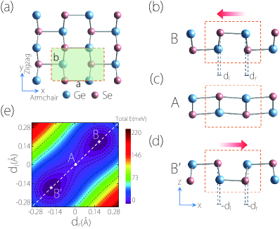
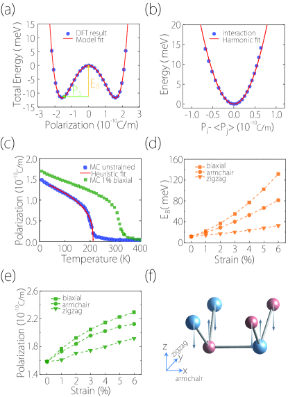
To investigate the lattice distortion that breaks the inversion symmetry, we define () to be the displacement between the neighbouring Ge and Se atoms along the armchair direction in the left (right) part of the unit cell, as indicated in Fig. 1(b). When , we have a centrosymmetric structure, denoted as the A state [see Fig. 1(c)], which forbids an electric polarization. In comparison, the stable structure in Fig. 1(b) has (denoted as B), and the finite displacements breaks the inversion symmetry. One also notes that via a spatial inversion operation, the B structure is mapped to the B’ shown in Fig. 1(d), which is also stable and degenerate with B in energy. Hence, B and B’ belong to a single (ferroelectric) phase. In Fig. 1(e), we plot the free-energy contours with respect to the two displacements and . The result shows that B and B’ indeed correspond to the two minimum points on the energy surface. They are connected through a saddle point which is just the centrosymmetric A state. This kind of double well structure is typical for ferroelectric materials, hence its appearance here strongly hints at possible ferroelectricity in monolayer -GeSe.
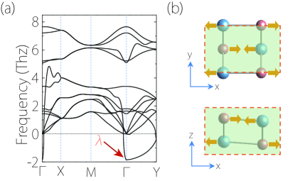
The instability towards lattice distortion for ferroelectric materials is often associated with the soft optical phonon modes for the undistorted structure which corresponds to the A state here. In Fig. 2(a), we plot the calculated phonon spectrum for the A state, in which one observes a pronounced soft optical mode at the BZ center . From the phonon eigenvector shown in Fig. 2(b), we find that this mode corresponds to the movement of neighboring atoms of the same atomic plane in opposite directions along with , which just leads to the distortion towards the non-centrosymmetric B or B’ structures.
Ferroelectricity in monolayer -GeSe is indeed confirmed by our DFT calculation using the Berry phase method King-Smith and Vanderbilt (1993); Resta (1994). The spontaneous polarization (per area of the 2D sheet) at zero temperature () is calculated to be 0.159 nC/m, which is comparable to the value for monolayer SnTe ( nC/m) Wan et al. (2017) that was successfully detected in recent experiment Chang et al. (2016). The corresponding bulk value is about 0.39 C/m2 if we estimate the effective thickness of the monolayer to be 0.41 nm von Rohr et al. (2017). The energy difference between the ferroelectric and the centrosymmetric states gives an estimation of the transition barrier , which is about 11.66 meV [5.83 meV per formula unit (f.u.)]. The obtained is much smaller than that for the conventional ferroelectric PbTiO3 ( 200 meV/f.u.) Cohen (1992), indicating that a much lower electric field is required to switch the direction of the electric polarization, which could be advantageous for achieving high energy efficiency for ferroelectric devices. It should be mentioned that a small energy barrier may lead to possible quantum tunneling effects. However, we note that for the confirmed 2D ferroelectric SnTe, the barrier is even smaller, meV/f.u. Wan et al. (2017). Yet the ferroelectricity in SnTe is stable up to 270 K, as demonstrated in experiment Chang et al. (2016). Therefore, we expect that the ferroelectricity in -GeSe can be robust.
| Material | |||||||
|---|---|---|---|---|---|---|---|
| -GeSe | 11.66 | 0.159 | -15.261 | 1.8389 | 1.7137 | 8.0904 | 212 |
Having confirmed the existence of ferroelectricity in monolayer -GeSe, we then check the stability of ferroelectricity by estimating its Curie temperature , above which the macroscopic spontaneous polarization is suppressed. Following the approach in Refs. Fei et al. (2016); Wan et al. (2017), we estimate using the MC method. A Landau-type theory is developed with the polarization taken as the order parameter. For this purpose, we need to map out the (, ) free-energy surface [as in Fig. 1(e)] as a function of . However, this is a computationally formidable task. Fortunately, one observes the steep gradients traverse to the diagonal line in Fig. 1(e) (marked by the white dashed line), which indicates that the structure prefers the so-called “-covariant” states with . Therefore, we may consider mapping only the one-dimensional subset of all configurations, leading to a significant reduction of the parameter space. The free energy curve along the -covariant line as a function of has been calculated and plotted in Fig. 3(a). Then we can construct a Landau-Ginzburg-type expansion of the total energy in the following form Fei et al. (2016); Wan et al. (2017):
| (1) |
where is the polarization of the -th unit cell, indicates the nearest neighbors, and , , , are constant coefficients. The first three terms capture the anharmonic double-well potential [see Fig. 3(a)]. The last term describes the dipole-dipole interaction between the nearest neighboring unit cells, which includes the geometry of the system and is crucial for phase transition. In Fig. 3(b), we show the comparison between the DFT result based on the supercell calculation and the fit using a quadratic function, which validates the harmonic approximation taken for the interaction term. All the coefficients in Eq. (1) are obtained by fitting the DFT results in the mean-field approximation Zhong et al. (1995); Fei et al. (2016), and their values are listed in Table 1.
With the effective model in Eq. (1), we can proceed to perform the MC simulation to investigate the temperature effects and the ferroelectric phase transition. The simulation results are plotted in Fig. 3(c). The intrinsic of monolayer -GeSe is estimated to be around 212 K. The average polarization in the vicinity of the transition follows a heuristic form with for , where is some constant and is the critical exponent. We fit MC simulation results with the heuristic form, and the obtained is around 0.347, which is lower than from the standard mean field theory of the 2D Ising model Fridkin and Ducharme (2014). This kind of behavior is consistent with the previous findings in Refs. Fei et al. (2016); Wan et al. (2017) for other 2D ferroelectric materials.
Before proceeding, we mention that in the MC approach, we did not consider the possible coupling term between the polarization and lattice strain, which is a standard approximation and yields good agreement between theory and experiment (e.g., for 2D SnTe, from such MC approach is K, very close to the experimental value of K) Wan et al. (2017); Chang et al. (2016). Here, to further consolidate our result, we perform the ab-initio molecular dynamics simulations, which give a result of K (see Supplemental Material SuppMater (2017)), which agrees well with the MC result.
III.2 Enhancement of ferroelectricity by strain
Strain engineering can effectively modify the electronic properties of 2D materials, and even produce remarkable quantum phase transitions, such as the bonding/nonbonding and magnetic phase transition in monolayer MoN2 Wang et al. (2016) as well as the semiconductor/topological-semimetal phase transition in blue phosphorene oxide Zhu et al. (2016). Effective strain tuning of ferroelectricity has also been demonstrated on the SrTiO3 thin films, where an enhancement of above room temperature has been observed Haeni et al. (2004).
Here we study the effects of three types of strain on the ferroelectric properties. These include the in-plane biaxial strain and the two uniaxial strains along armchair and zigzag directions. In Figs. 3(d,e), we plot the transition energy barrier and the polarization as functions of the applied strain. One observes that the biaxial and the uniaxial tensile strain along the armchair direction can enlarge both and , which can be expected by noticing that both strains tend to increase the relative displacements and between Ge and Se atoms. At 6% biaxial strain, the value of can be increased by more than 40% to 0.23 nC/m. Interestingly, we find that the the uniaxial tensile strain along the zigzag direction also increases and . This seemingly counterintuitive behavior is originated from the puckered lattice structure. As illustrated in Fig. 3(f), the tensile strain along the zigzag direction tends to pull the ions towards the same - plane, decreasing the distance between the neighboring atomic sites along the -direction. Then the repulsion between the ions (which tends to maintain the bond length) will lead to increased relative displacement between the neighbors along the -direction, thereby increasing and .
The enhancement in and by strain will also increase the Curie temperature. We repeat the MC simulations for the strained monolayer -GeSe. The result indeed shows that is increased by the applied strain. Excitingly, the enhancement is quite significant. For example, under a 1% biaxial strain, can already be increased to about 320 K, above the room temperature [see Fig. 3(c)]. This implies the great potential for the application of monolayer -GeSe in ferroelectric devices, and its sensitive strain dependence also allows promising applications in mechanical sensors.
III.3 Strain controlled anisotropic transport and Lifshitz transition
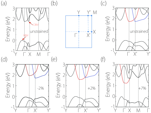
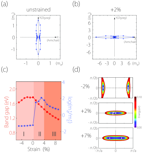
In the following, we focus on the electronic band structure of monolayer -GeSe. The DFT result of the band structure is plotted in Fig. 4(a). One observes that it has a indirect band gap about 1.77 eV with conduction band minimum (CBM) (marked by red arrow) located on the -X path, whereas the valence band maximum (VBM) is on the -Y path. As illustrated in Fig. 4(b), we label the location of CBM by X’. To see the band dispersion around CBM (X’ point) more clearly, we re-plot the band structure along the new route in Fig. 4(c), which includes the dispersion along the perpendicular direction X’-Y’. Interestingly, the band dispersion is highly anisotropic around the CBM (marked by the blue color): the band is highly dispersive along the -X’ direction, whereas its dispersion is quite small along the X’-Y’ direction. The -X’ and X’-Y’ paths correspond to the armchair and the zigzag directions in real space. The large difference in the dispersions reflects the anisotropy in the lattice structure. As a result, the effective mass of the electron carriers, which are proportional to the inverse of the curvature of the band dispersion, are also highly anisotropic. We plot the electron effective mass along different in-plane directions in Fig. 5(a), which shows an approximate “8” shape. The values of the effective mass of electrons differ by an order of magnitude for the two orthogonal directions: the effective mass along the armchair direction is about 0.086 ( is the bare electron mass), whereas the effective mass along the zigzag direction is about 1.392.
Interestingly, we find that an applied strain can switch the anisotropy in dispersion by 90∘. In Fig. 4(c), one observes that there is another conduction band (marked by the red color) with a band minimum located at the point, the energy of which is only slightly above CBM. Moreover, the dispersion of this red-colored band is also highly anisotropic: it is highly dispersive along the -Y (zigzag) direction while nearly flat along the -X’ (armchair) direction. The anisotropy pattern is orthogonal to that of the blue-colored band. (These features have also been confirmed by our calculations using the hybrid functional (HSE06) Heyd et al. (2003). See the Supplemental Material SuppMater (2017).) Hence the anisotropic dispersion of the electron carriers will be dramatically changed if the orderings of these two colored bands are switched. In the following, we show that the applied strain can readily generate this band switching and hence change the anisotropy in the carrier dispersion.
In Fig. 4(d-f), we show the band structure results with applied uniaxial strains along the zigzag direction. One observes that a compressive strain can shift the red-colored band up relative to the blue-colored one, whereas a tensile strain can pull the red-colored band below the blue-colored one. Figure 4(e) shows that a small (2%) tensile strain can switch the CBM from X’ to . (The transition occurs at a critical strain less than 1%.) Comparing Fig. 4(d) and Fig. 4(e), one observes that the dispersions of the two bands near their respective minima are almost unchanged. In Fig. 5(b), we plot the electron effective mass variation for the strained sample (corresponding to Fig. 4(e)). One indeed observe that the anisotropy is rotated by 90∘ compared to the unstrained case: now whereas . If we take the ratio as a measure of the anisotropy, then its values changes dramatically from for the intrinsic (unstrained) case to for the strained case. The change is above 600 times. In Fig. 5(c), we plot the ratio along with the variation of the bandgap versus the applied strain. One clearly observes the abrupt jump at the critical strain when the CBM is switched between the two bands (i.e., between I and II).
For the electron doped case, the switch of band ordering discussed above is accompanied by a transformation of the Fermi surface topology, i.e., a Lifshitz transition. And our result shows that there also appear interesting valley features in the conduction band. In Fig. 5(d), we plot the equi-energy contours around the CBM for three representative strains. One observes that at strain, there are two separate valleys located on the -X path, related by the time reversal symmetry. At strain, the CBM is switched to , hence there is only one valley. In addition, at even larger strains (% strain in Fig. 5(d)), the single valley at further split into two along the -X path, corresponding to the band structure in Fig. 4(f). The three cases in Fig. 5(d) correspond to the three different shaded regions in Fig. 5(c).
In the above discussion, we focus on the uniaxial strain along the zigzag direction. These effects can also be achieved by biaxial strain or uniaxial strain along the armchair direction. We find that the results for the armchair uniaxial strain and the biaxial strain are similar to that for the zigzag uniaxial strain (see Supplemental Material SuppMater (2017)).
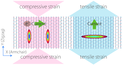
The strong anisotropy in the band dispersion will be reflected in electric transport. For example, the small ratio for the unstrained or compressed case indicates that the electric conduction (conductivity) is easier (larger) in the armchair direction. Across the transition from Region I to Region II in Fig. 5(c), the easy-conduction direction is switched to the zigzag direction. These two scenarios are schematically shown in Fig. 6. The sudden change induced by strain can be directly probed in the electric transport measurement. In addition, the abrupt change in Fermi surface topology discussed above can be probed as the change in magnetic quantum oscillations (like the Shubnikov-de Haas oscillations) under strain.
IV Discussion and conclusion
As we have mentioned, the 3D bulk -GeSe have already been synthesized in experiment and is stable under ambient conditions von Rohr et al. (2017). This would greatly facilitate the realization of the 2D monolayer, e.g., by using the mechanical exfoliation method. Experimentally, it has been demonstrated that the structurally similar Group-IV monochalcogenides can be thinned down to few layers by mechanical exfoliation Ye et al. (2017). Therefore, we expect that monolayer -GeSe could also be fabricated in the near future. Once realized, the ferroelectricity can be detected by the standard probes, such as the synchrotron X-ray scattering Fong et al. (2004), ultraviolet Raman spectroscopy Tenne et al. (2009), polarized second-harmonic generation measurement Sheng et al. (2010), piezoresponse force microscope Garcia et al. (2009), and STM/STS measurements Chang et al. (2016).
Electronic and optical properties of -GeSe were also theoretically studied in Ref. 37, in which the strong anisotropy in carrier transport and the strain effects on the bandgap where reported. In comparison, the present work reveals that strain can tune the ferroelectricity to a large extent, switch the anisotropy in carrier transport, and induce interesting Lifshiftz transition for doped samples, associated with changes in the valley configurations. These points have not been addressed before.
Techniques for applying strain on 2D materials have been well developed. For example, strain can be applied by using the beam bending apparatus Conley et al. (2013) or by using the AFM tips Lee et al. (2008). Generally, tensile strains would be easier to apply than compressive strains, because 2D materials tend to buckle under compression. Experimentally, small compressive strains may be achieved by attaching the 2D sample to substrate and applying compression on the substrate.
2D materials typically have excellent mechanical flexibility. For example, graphene, MoS2, and black phosphorene can sustain strains above 25% Lee et al. (2008); Castellanos-Gomez et al. (2012); Bertolazzi et al. (2011); Peng et al. (2014). Experimentally, strains above 15% have been demonstrated Lee et al. (2008); Kim et al. (2009). For monolayer -GeSe, our estimation shows that its critical tensile stain can be up to 16% (see Supplemental Material SuppMater (2017)). We have calculated the Young s modulus, which is about 83 GPa along the zigzag direction and about 85 GPa along the armchair direction. These values are comparable to that of phosphorene ( GPa along the zigzag direction and GPa along the armchair direction) Wei et al. (2014), and is less than that for graphene ( GPa) Lee et al. (2008) and MoS2 ( GPa) Castellanos-Gomez et al. (2012). These results indicate the feasibility of the strain engineering on -GeSe discussed in this work.
The major band structure features discussed in Sec. III.3 have been checked by our calculations including SOC or using hybrid functional method (see Supplemental Material SuppMater (2017)). Hence our predictions are robust. The band-switching transition occurs at a very small strain around . Similar strain effect on anisotropic transport was also predicted in monolayer black phosphorene Fei and Yang (2014). We mention that, for monolayer -GeSe, the required strain for the switching is much smaller than that in monolayer black phosphorene () Fei and Yang (2014). This could make the effect for monolayer -GeSe more easily observed in experiment.
In conclusion, based on first-principles calculations, we have demonstrated ferroelectricity in monolayer -GeSe. We find that the spontaneous polarization and the transition energy barrier can be significantly enhanced by various types of strains. The Curie temperature is estimated to be 212 K, and it can be increased above room temperature by applying a tensile strain. From band structure analysis, we identify highly anisotropic dispersions for the electron carriers. We find that the preferred conduction direction can be rotated by under strain. Particularly, the ratio between the effective masses along the two in-plane directions can undergo a abrupt change of two orders of magnitude by a 2% strain. For electron doped case, the effect is associated with a strain-induced Lifshitz transition and there also appear interesting valley features in the band structure. Our findings thus provide a promising platform to explore the intriguing physics of ferroelectricity in two dimensions and reveal the great potential of -GeSe for the nanoscale mechano-electronic device applications.
Acknowledgements.
The authors thank D.L. Deng for helpful discussions. The work is supported by the MOST Project of China (Grants No. 2014CB920903), the NSF of China (Grants Nos.11574029, 11734003), the National Key R&D Program of China (Grant No.2016YFA0300600), the Singapore Ministry of Education Academic Research Fund Tier 1 (SUTD-T1-2015004). We acknowledge computational support from the Texas Advanced Computing Center and the National Supercomputing Centre Singapore.References
- Setter et al. (2006) N. Setter, D. Damjanovic, L. Eng, G. Fox, S. Gevorgian, S. Hong, A. Kingon, H. Kohlstedt, N. Y. Park, G. B. Stephenson, I. Stolitchnov, A. K. Taganstev, D. V. Taylor, T. Yamada, and S. Streiffer, Journal of Applied Physics 100, 051606 (2006), .
- Scott (2007) J. F. Scott, Science 315, 954 (2007), .
- Nuraje and Su (2013) N. Nuraje and K. Su, Nanoscale 5, 8752 (2013).
- Batra et al. (1973) I. P. Batra, P. Wurfel, and B. D. Silverman, Phys. Rev. Lett. 30, 384 (1973).
- Zhong et al. (1994) W. Zhong, D. Vanderbilt, and K. M. Rabe, Phys. Rev. Lett. 73, 1861 (1994).
- Dawber et al. (2005) M. Dawber, K. M. Rabe, and J. F. Scott, Rev. Mod. Phys. 77, 1083 (2005).
- Castro Neto et al. (2009) A. H. Castro Neto, F. Guinea, N. M. R. Peres, K. S. Novoselov, and A. K. Geim, Rev. Mod. Phys. 81, 109 (2009).
- Butler et al. (2013) S. Z. Butler, S. M. Hollen, L. Cao, Y. Cui, J. A. Gupta, H. R. Guti茅rrez, T. F. Heinz, S. S. Hong, J. Huang, A. F. Ismach, E. Johnston-Halperin, M. Kuno, V. V. Plashnitsa, R. D. Robinson, R. S. Ruoff, S. Salahuddin, J. Shan, L. Shi, M. G. Spencer, M. Terrones, W. Windl, and J. E. Goldberger, ACS Nano 7, 2898 (2013) .
- Tan et al. (2017) C. Tan, X. Cao, X.-J. Wu, Q. He, J. Yang, X. Zhang, J. Chen, W. Zhao, S. Han, G.-H. Nam, M. Sindoro, and H. Zhang, Chemical Reviews 117, 6225 (2017) .
- Shirodkar and Waghmare (2014) S. N. Shirodkar and U. V. Waghmare, Phys. Rev. Lett. 112, 157601 (2014).
- Di Sante et al. (2015) D. Di Sante, A. Stroppa, P. Barone, M.-H. Whangbo, and S. Picozzi, Phys. Rev. B 91, 161401 (2015).
- Noor-A-Alam and Shin (2016) M. Noor-A-Alam and Y.-H. Shin, Phys. Chem. Chem. Phys. 18, 20443 (2016).
- Ding et al. (2017) W. Ding, J. Zhu, Z. Wang, Y. Gao, D. Xiao, Y. Gu, Z. Zhang, and W. Zhu, Nature Communications 8, 14956 (2017).
- Wu and Zeng (2016) M. Wu and X. C. Zeng, Nano Letters 16, 3236 (2016).
- Fei et al. (2016) R. Fei, W. Kang, and L. Yang, Phys. Rev. Lett. 117, 097601 (2016).
- Wang and Qian (2017) H. Wang and X. Qian, 2D Materials 4, 015042 (2017).
- Wan et al. (2017) W. Wan, C. Liu, W. Xiao, and Y. Yao, Applied Physics Letters 111, 132904 (2017) .
- Chengcheng Xiao (2017) C. C. Xiao, F. Wang, S. A. Yang, Y. H. Lu, Y. P. Feng, S. B. Zhang, Adv. Funct. Mater. 1707383 (2018) .
- Chang et al. (2016) K. Chang, J. Liu, H. Lin, N. Wang, K. Zhao, A. Zhang, F. Jin, Y. Zhong, X. Hu, W. Duan, Q. Zhang, L. Fu, Q.-K. Xue, X. Chen, and S.-H. Ji, Science 353, 274 (2016) .
- Zhou et al. (2017) Y. Zhou, D. Wu, Y. Zhu, Y. Cho, Q. He, X. Yang, K. Herrera, Z. Chu, Y. Han, M. C. Downer, H. Peng, and K. Lai, Nano Letters 17, 5508 (2017)
- von Rohr et al. (2017) F. O. von Rohr, H. Ji, F. A. Cevallos, T. Gao, N. P. Ong, and R. J. Cava, Journal of the American Chemical Society 139, 2771 (2017).
- Li et al. (2014) L. Li, Y. Yu, G. J. Ye, Q. Ge, X. Ou, H. Wu, D. Feng, X. H. Chen, and Y. Zhang, Nat Nano 9, 372 (2014).
- Peng et al. (2014) X. Peng, Q. Wei, and A. Copple, Phys. Rev. B 90, 085402 (2014).
- Jiang and Park (2014) J.-W. Jiang and H. S. Park, Nature Communications 5, 4727 (2014).
- Fei and Yang (2014) R. Fei and L. Yang, Nano Letters 14, 2884 (2014) .
- Lu et al. (2016) Y. Lu, D. Zhou, G. Chang, S. Guan, W. Chen, Y. Jiang, J. Jiang, X.-s. Wang, S. A. Yang, Y. P. Feng, Y. Kawazoe, and H. Lin, npj Computational Materials 2, 16011 (2016) .
- Blöchl (1994) P. E. Blöchl, Phys. Rev. B 50, 17953 (1994).
- Kresse and Hafner (1993) G. Kresse and J. Hafner, Phys. Rev. B 47, 558 (1993).
- Kresse and Furthmüller (1996) G. Kresse and J. Furthmüller, Phys. Rev. B 54, 11169 (1996).
- Perdew et al. (1996) J. P. Perdew, K. Burke, and M. Ernzerhof, Phys. Rev. Lett. 77, 3865 (1996).
- Togo and Tanaka (2015) A. Togo and I. Tanaka, Scripta Materialia 108, 1 (2015).
- King-Smith and Vanderbilt (1993) R. D. King-Smith and D. Vanderbilt, Phys. Rev. B 47, 1651 (1993).
- Resta (1994) R. Resta, Rev. Mod. Phys. 66, 899 (1994).
- Zhong et al. (1995) W. Zhong, D. Vanderbilt, and K. M. Rabe, Phys. Rev. B 52, 6301 (1995).
- Grimme (2006) S. Grimme, J.Comput.Chem. 27, 1787 (2006) .
- SuppMater (2017) See Supplemental Material at http://link.aps.org/supplemental/xxx/PhysRevB.xxx for the phonon spectrum, strain-stress relation, ab-initio MD simulation result, band structure with SOC included and with HSE06 method, band feature variation under other types of strains for monolayer -GeSe .
- Yuanfeng Xu and Zhu (2017) Y. F. Xu, H. Zhang, H. Z. Shao, G. Ni, J. Li,H. L. Lu, R. J. Zhang, B. Peng, Y. Y. Zhu, H. Y. Zhu, and C. M. Soukoulis, Phys. Rev. B 96, 245421 (2017).
- Cohen (1992) R. E. Cohen, Nature 358, 136 (1992).
- Fridkin and Ducharme (2014) V. Fridkin and S. Ducharme, Ferroelectrics 466, 133 (2014) .
- Wang et al. (2016) Y. Wang, S.-S. Wang, Y. Lu, J. Jiang, and S. A. Yang, Nano Letters 16, 4576 (2016) .
- Zhu et al. (2016) L. Zhu, S.-S. Wang, S. Guan, Y. Liu, T. Zhang, G. Chen, and S. A. Yang, Nano Letters 16, 6548 (2016).
- Haeni et al. (2004) J. H. Haeni, P. Irvin, W. Chang, R. Uecker, P. Reiche, Y. L. Li, S. Choudhury, W. Tian, M. E. Hawley, B. Craigo, A. K. Tagantsev, X. Q. Pan, S. K. Streiffer, L. Q. Chen, S. W. Kirchoefer, J. Levy, and D. G. Schlom, Nature 430, 758 (2004).
- Heyd et al. (2003) J. Heyd, G. E. Scuseria, and M. Ernzerhof, The Journal of Chemical Physics 118, 8207 (2003).
- Ye et al. (2017) Y. Ye, Q. Guo, X. Liu, C. Liu, J. Wang, Y. Liu, and J. Qiu, Chemistry of Materials 29, 8361 (2017) .
- Fong et al. (2004) D. D. Fong, G. B. Stephenson, S. K. Streiffer, J. A. Eastman, O. Auciello, P. H. Fuoss, and C. Thompson, Science 304, 1650 (2004) .
- Tenne et al. (2009) D. A. Tenne, P. Turner, J. D. Schmidt, M. Biegalski, Y. L. Li, L. Q. Chen, A. Soukiassian, S. Trolier-McKinstry, D. G. Schlom, X. X. Xi, D. D. Fong, P. H. Fuoss, J. A. Eastman, G. B. Stephenson, C. Thompson, and S. K. Streiffer, Phys. Rev. Lett. 103, 177601 (2009).
- Sheng et al. (2010) Z. Sheng, N. Ogawa, Y. Ogimoto, and K. Miyano, Adv. Mater. 22, 5507 (2010).
- Garcia et al. (2009) V. Garcia, S. Fusil, K. Bouzehouane, S. Enouz-Vedrenne, N. D. Mathur, A. Barthelemy, and M. Bibes, Nature 460, 81 (2009).
- Conley et al. (2013) H. J. Conley, B. Wang, J. I. Ziegler, R. F. Haglund, S. T. Pantelides, and K. I. Bolotin, Nano Letters 13, 3626 (2013) .
- Wei et al. (2014) Q. Wei, and X. H. Peng, Appl. Phys. Lett. 104, 251915 (2014).
- Lee et al. (2008) C. Lee, X. Wei, J. W. Kysar, and J. Hone, Science 321, 385 (2008) .
- Castellanos-Gomez et al. (2012) A. Castellanos-Gomez, M. Poot, G. A. Steele, H. S. van der Zant, N. Agraït, and G. Rubio-Bollinger, Nanoscale Research Letters 7, 233 (2012).
- Bertolazzi et al. (2011) S. Bertolazzi, J. Brivio, and A. Kis, ACS Nano 5, 9703 (2011).
- Kim et al. (2009) K. S. Kim, Y. Zhao, H. Jang, S. Y. Lee, J. M. Kim, K. S. Kim, J.-H. Ahn, P. Kim, J.-Y. Choi, and B. H. Hong, Nature 457, 706 (2009).