Fabrication of (111)-Faced Single-Crystal Diamond Plates
by Laser Nucleated Cleaving
Abstract
Single-crystal diamond plates with surfaces oriented in a (111) crystal plane are required for high-performance solid-state device platforms ranging from power electronics to quantum information processing architectures. However, producing plates with this orientation has proven challenging. In this paper, we demonstrate a method for reliably and precisely fabricating (111)-faced plates from commercially available, chemical-vapor-deposition-grown, type-IIa single-crystal diamond substrates with (100) faces. Our method uses a nanosecond-pulsed visible laser to nucleate and propagate a mechanical cleave in a chosen (111) crystal plane, resulting in faces as large as with atomically flat surfaces, negligible miscut angles, and near zero kerf loss. We discuss the underlying physical mechanisms of the process along with potential improvements that will enable the production of millimeter-scale (111)-faced single-crystal diamond plates for a variety of emerging devices and applications.
keywords:
single-crystal diamond, cleaving, (111) orientation, surface roughness1 Introduction
Advances in homoepitaxial chemical vapor deposition (CVD) of high-purity single-crystal diamond (SCD) have made the exceptional material properties of SCD available for a variety of new and exciting applications [1, 2, 3, 4]. In particular, the wide bandgap, high carrier mobility, large thermal conductivity, corrosion resistance, and biocompatibility of SCD have enabled new devices for high-power electronics [5], ultraviolet light sources [6] and detectors [7], nonlinear optics [8, 9, 10], quantum information processing [11], biomedical applications [12, 13], magnetometry [14], and integrated photonics [15, 16, 17, 18, 19].
Many of these diverse applications benefit from the advantageous mechanical, thermal, and bond properties along . For example, the (111) crystal plane is the hardest face [20, 21], making it more resilient to damage and desirable for industrial scale diamond cutting tools [1]. Similarly, the Raman gain coefficient is strongest when the optical polarization axis is aligned along [22, 23]. For this reason, integrating on-chip Raman lasers requires precise crystallographic orientation of the diamond layer to maximize the laser efficiency [10]. High-power electronic devices also benefit from (111) faces, which provide improved donor incorporation efficiency and correspondingly higher mobility [24, 25, 26, 27, 5, 28]. Finally, point defects in SCD that are used as single-photon sources and spin qubits, such as the nitrogen-vacancy and silicon-vacancy centers, have a symmetry axis aligned along directions [29, 30, 31, 32]. Thus, a (111) face maximizes the interaction with normally-incident light fields and optimizes the photon collection efficiency from these emitters, which is critically important for light-matter quantum interfaces [33] and high-sensitivity magnetometry [34, 35].
While (100)-faced SCD plates are commonly produced by homoepitaxial CVD, growth of (111)-faced SCD plates has proven challenging due to twinning and stacking faults that form along directions [36, 2, 28]. Despite some recent advances [4, 37], inherent challenges still remain in growing (111)-oriented layers thicker than with low surface roughness. For this reason, macroscopic (111)-faced plates are typically cut from larger (100)-faced starting plates using micro-machining laser ablation tools [38] and subsequent polishing steps are used to reduce the surface roughness [39, 40]. This process results in substantial loss of costly SCD material (kerf loss) along with misalignment of the resulting face relative to [111], since it is nearly impossible to polish the (111) face using traditional methods [20]. Furthermore, the mechanical polishing step induces sub-surface damage that can only be removed by further chemical etching [36].
An alternate approach, traditionally used to shape diamond gemstones, is mechanical cleaving, where a small scribe, or kerf, is created and struck by hand with a knife to initiate a cleave. It is not feasible, however, to perform this process by hand with the micron-scale accuracy needed to create large, thin, parallel plates for electronic and optical applications from small samples of SCD. Instead, it would be valuable to establish a process similar to silicon stealth dicing [41], whereby a laser is used to nucleate and propagate a mechanical cleave with high spatial precision and control of the cleaving dynamics.
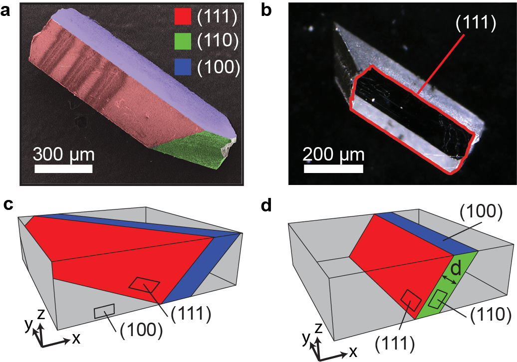
In this paper, we present a laser-nucleated cleaving (LNC) process for SCD. Rather than machining the entire surface of a desired face, the LNC process uses a pulsed, focused laser with sub-bandgap photon energy () to locally graphetize a thin ( diameter) line that propagates a mechanical cleave along a desired (111) plane. As shown in Fig. 1, (111)-faced plates are fabricated by generating two parallel (111) cleave planes, forming a parallelepiped shape. This process results in large, atomically-flat (111)-faced SCD plates while eliminating kerf loss and removing the need for mechanical polishing.
The paper is organized as follows: first, a step-by-step description of the LNC process is provided, followed by atomic force microscopy (AFM) and X-ray diffraction measurements that determine the surface roughness and confirm the crystal orientation, respectively. Then, the potential physical mechanisms that contribute to the LNC process are discussed. Finally, avenues for improving the process to optimize the size and flatness of (111)-faced SCD plates are presented.
2 Materials and methods
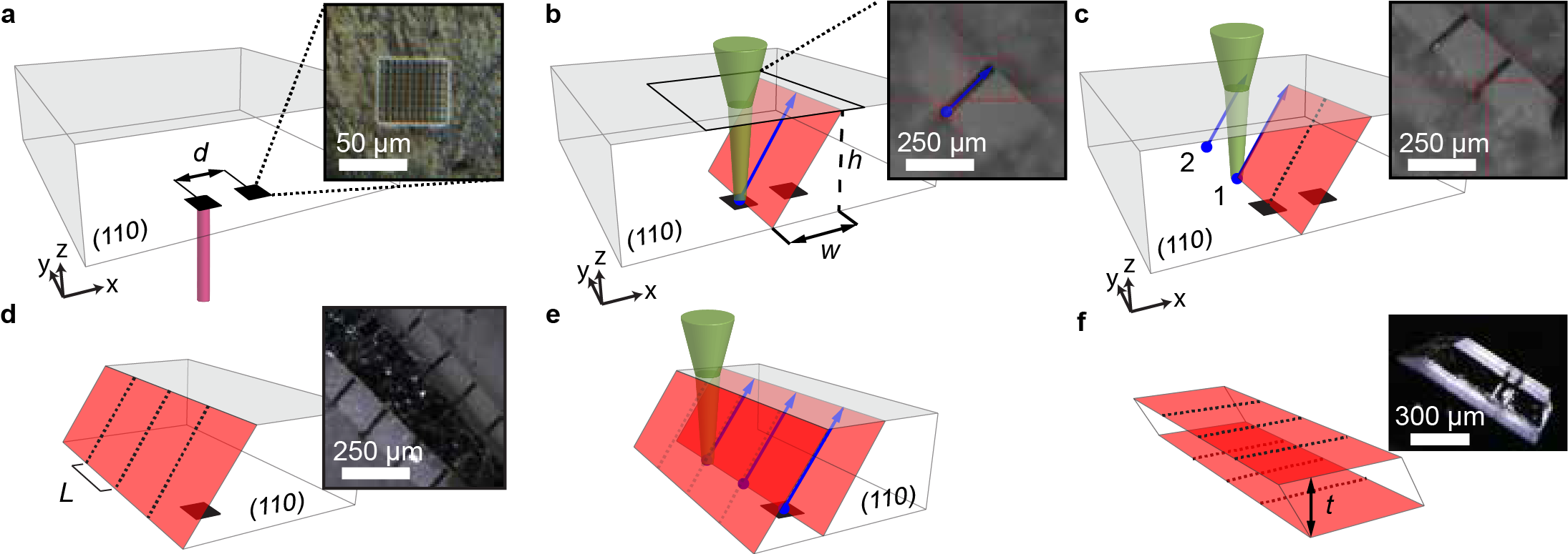
The LNC process is illustrated in Fig. 2 and the individual steps are described in the section below. We begin by discussing the types of SCD plates used in this study followed by the micro-machining laser specifications. Then, we outline the LNC process which is grouped into four sub-processes consisting of nucleation site creation, initiation of the cleave, propagating the cleave front, and backside cleaving to produce a free standing (111)-faced SCD plate. Finally, the details concerning the characterization of the SCD plates’ physical properties are covered. Additional details are included in the supporting information [42].
2.1 Materials
2.2 Nucleation site creation
The LNC process begins with the creation of a nucleation site on the bottom surface of the starting SCD plate. The nucleation site acts as a seed for producing the initial cleave. For samples with two polished (100) faces, textured regions [Fig. 2(a), inset] are laser-machined onto the backside using an excimer laser [42]. Only one textured site per desired (111) face is required. For single-side polished pieces, the unpolished side of as-received samples with a surface roughness of [43] was found to be sufficient to nucleate cleaves without any additional patterning.
2.3 Micromachining laser beam preparation
We perform LNC using a nanosecond pulsed, frequency-doubled Yb-doped fiber laser operating at a wavelength of with a repetition rate of , integrated in a micromachining laser system (IPG Photonics, IX-280-ML). The primary focusing optic is a -focal-length objective that produces a beam waist of diameter , a beam quality factor of , and a depth of field . In this system, the laser focus and course lateral position are controlled using a motorized stage, and cuts are made by steering the beam with a galvo scanner. The starting SCD plate is fixed to a -thick glass microscope slide with double-sided tape so that the micromaching laser can be focused through the air/diamond interface (referred to as the top surface) onto the tape-diamond interface (referred to as the bottom surface).
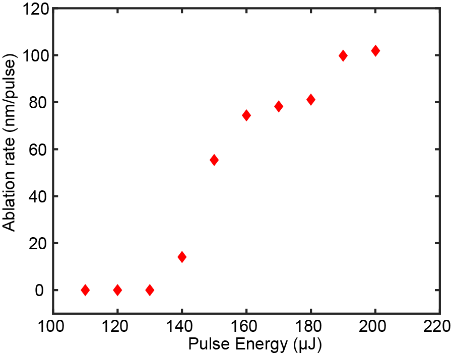
The beam focus is positioned such that the bottom surface of the SCD plate ablates while the top surface does not. SCD ablation by sub-bandgap light is a nonlinear optical process, and the ablation rate depends sensitively on the pulse fluence [44]. Positioning the laser focus close to the bottom surface establishes a fluence gradient such that the top surface is unaffected by the micromaching laser beam, whereas the bottom surface is above the threshold for ablation and graphetization. The presence of a nucleation site or unpolished bottom surface further lowers the threshold for ablation. Figure 3 depicts the experimentally measured ablation rate of a top polished SCD surface as a function of pulse energy for our micromaching laser, exhibiting an abrupt threshold around .
2.4 Initiating the cleave
To initiate a cleave, the micromachining laser beam is aligned over a textured nucleation site, or a target region of an unpolished bottom surface using the sample stage. The laser beam is then switched on and laterally scanned in at a speed of by a distance , as illustrated in Fig. 2(b). The scan distance is calculated according to , where is the starting SCD plate thickness, and is the angle between the [111] and [100] lattice vectors. This translation distance ensures that the cleave extends through the full thickness of the SCD (- plane). After this step, a darkened line appears and a new reflective surface can be seen within the diamond [Fig. 2(b), inset]. The combination of these two observations heralds the presence of a cleave along a (111) face.
2.5 Propagating the cleave
As seen in Fig. 2(b), a typical cleave only propagates a few hundred microns away from the laser scan line in the -direction. The (111) crystal face is extended by repeating the lateral laser scans used in the previous step, but with the beam translated along near the edge of the newly-created (111) face. Scanning the laser again along extends the cleave further along , as shown in Fig. 2(c). As such, a textured nucleation site is only required at the position of the first laser scan line to initiate a cleavage plane. After each subsequent extension of the (111) face, a new boundary is identified in the microscope and the laser scan process is repeated until the cleave has been extended across the entire width of the starting SCD plate, creating a fully exposed (111) face [Fig. 2(d)].
2.6 Backside cleaving
To complete the (111)-faced SCD plate fabrication, a second (111) crystal face is generated that is parallel to the initial exposed face. The distance between the two nucleation sites sets the resulting plate thickness as can be seen in Fig. 2(f). For reliable performance, we find that the second nucleation site should be offset by a distance greater than the beam translation distance, () [Fig. 2(e)], hence the minimum (111)-faced plate thickness is limited by the starting plate height, .
2.7 Characterization
Measurements of the cleaved-face lattice orientation were made at room temperature using X-Ray diffraction with a source, a divergence slit, scatter slit, receiving slit, and a scintillator detector. Plates were mounted on a glass slide using crystal bond. Surface roughness was characterized using an Asylum MFP-3D atomic-force scanning probe with -axis noise (average deviation) in a - bandwidth.
3 Results
3.1 Plate dimensions
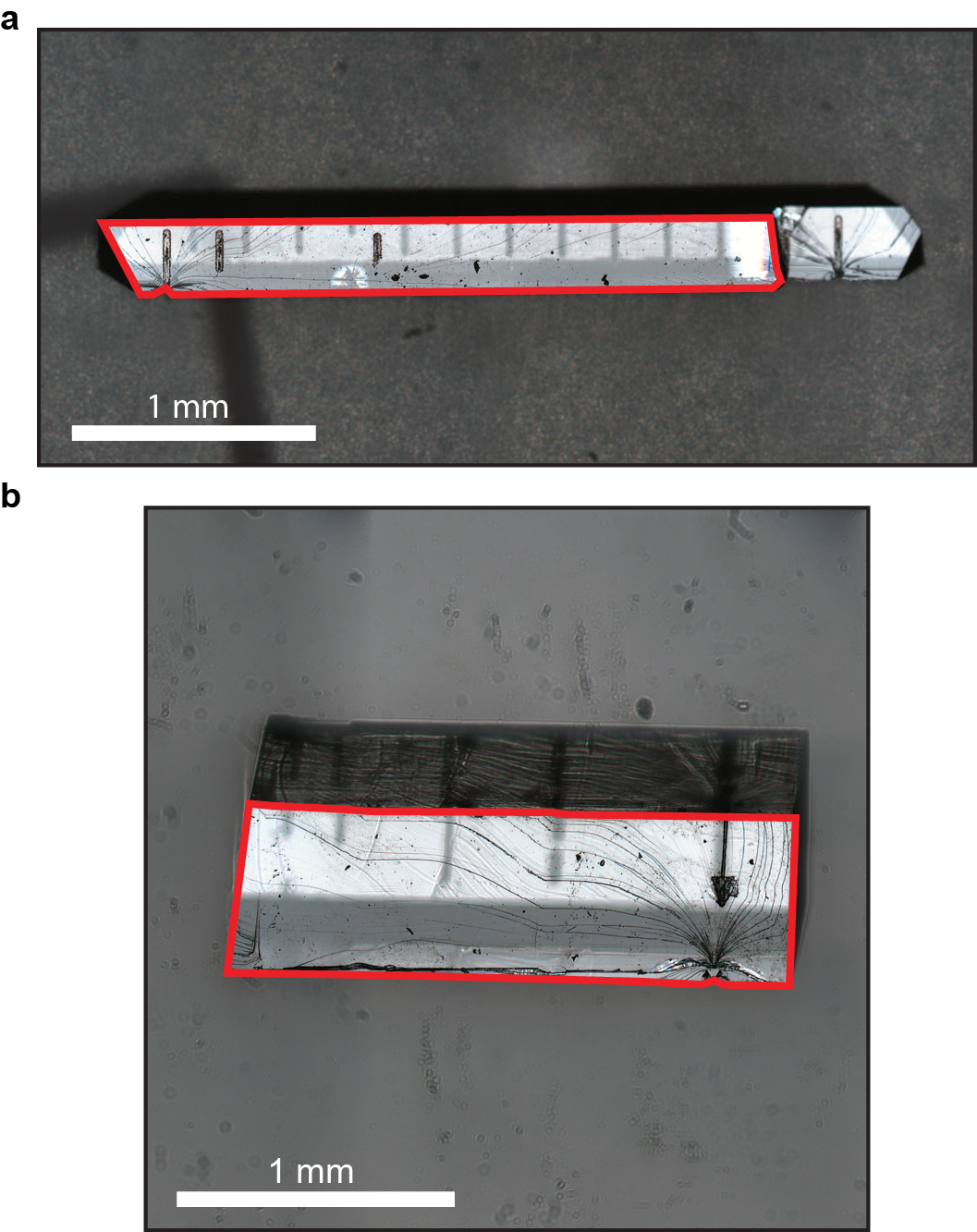
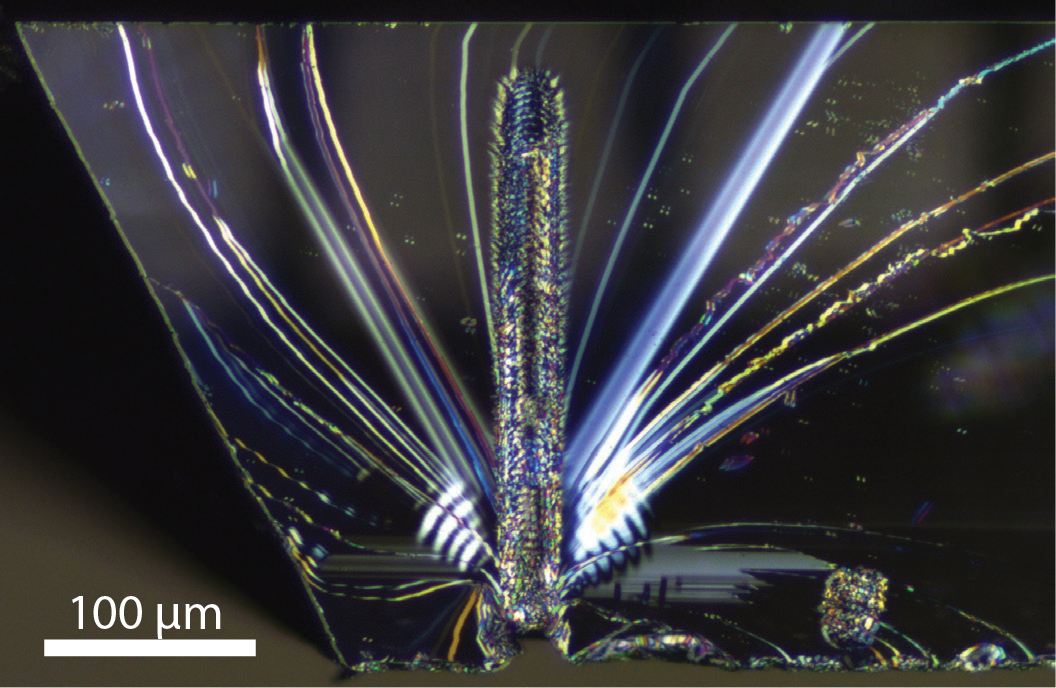
Representative (111)-faced plates produced by the LNC process are shown in Fig. 1(a)-(b), Fig. 2(f), and Fig. 4. The dark lines on the top and bottom surfaces of the plates are the locations of the micromachining laser scan lines. A laser-scan-line separation in of was found to be suitable for reliably propagating the cleave using an automated process [Fig. 4, bottom surface]. However, by manually identifying the cleavage plane boundary in the microscope, much larger spacings can be realized [Fig. 4, top surface], resulting in laser-scan-line-free areas ranging from 2 [Fig. 2(f) inset] to 2 [Fig. 4(b)].
Fabricated plate thicknesses vary from [Fig. 2(f) inset] to [Fig. 4(b)]. Minimum thicknesses of and are reliably produced for starting plate thicknesses of and , respectively. A single (100) SCD plate can typically yield up to 10 (111)-faced plates. The number is limited due to the increasing number of stochastically-generated cracks along undesired planes as the original SCD plate is diced into multiple (111)-faced plates.
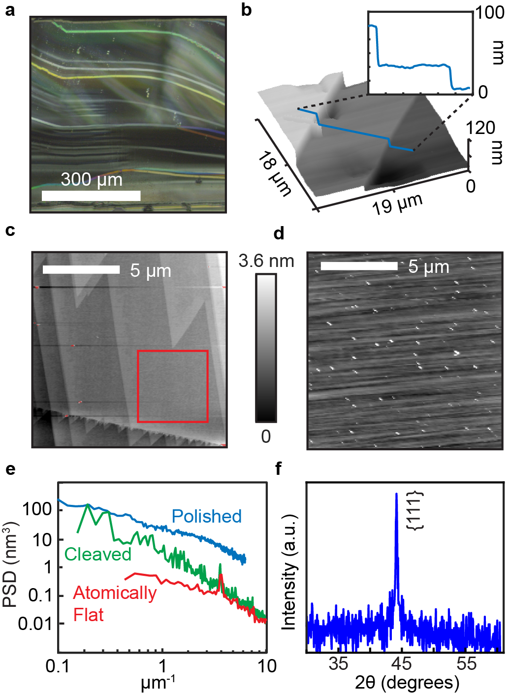
3.2 Surface Morphology
Lines running along the (111) face in the direction of the cleave propagation can be observed in the differential-interference-contrast optical microscope image shown in Fig. 5(a). These nanometer-scale steps or ridges are known as Wallner lines, which appear ubiquitously on cleaved surfaces of brittle materials as a result of the interaction between the crack front and transverse acoustic waves [45, 39]. Using atomic force microscopy (AFM), we find that the Wallner lines typically exhibit step heights of 10– [Fig 5(b)], with separations that vary from near the initial laser scan line to in regions farther away.
As shown in Fig. 5(c), the areas between Wallner lines exhibit atomically-flat (111) surfaces characterized by micron-scale, triangular terraces with step heights consistent with the expected spacing of (111) atomic planes [4]. The terraces are occasionally intersected by linear features as observed in the bottom-left of Fig. 5(c). For comparison, the polished (100) surface of an EG-SCD plate, as-received from the manufacturer [43] following cleaning using an acid bath and O2 plasma treatment, is displayed in Fig. 5(d).
Clearly, the morphologies of the cleaved and polished surfaces are very different. Figure 5(e) shows the power spectral density (PSD) of the AFM scans in Figs. 5(c,d), as well as the PSD for the region of a single atomic plateau indicated by a red box in Fig. 5(c). Over the entire AFM scan windows, we calculate root-mean-square (RMS) surface roughness values of and for the cleaved (111) and polished (100) surfaces, respectively. The LNC surface roughness represents an order-of-magnitude improvement compared to the manufacturer’s specification for the polished surface (average roughness ) and a smoothness comparable to the best values reported from advanced polishing techniques of [46]. Furthermore, the majority of the cleaved-surface roughness occurs in the form of atomic steps with micron-scale spacings, whereas the polished surface exhibits roughness over a broad range of spatial frequencies. The calculated RMS roughness of the region on an atomic terrace is , corresponding to the noise floor of the AFM tool. Further details the AFM surface roughness analysis are provided in the supporting information [42].
3.3 Face Orientation
Crystallographic faces were indexed using X-ray diffraction [Fig. 5(f)], showing a peak at that corresponds to first order Bragg diffraction from {111} planes. Since the spacing between individual (111) planes is , where is the lattice constant of diamond, the first (111) diffraction peak should appear at . These measurements have insufficient accuracy to determine the miscut angle, but we can use the features in AFM scans like Fig. 5(b)-(c) to estimate the miscut based on the heights and spacings of atomically-flat plateaus. In between Wallner lines, we typically observe atomic terraces with spacings, corresponding to a miscut angle of . Over larger length scales, Wallner lines of height are typically separated by , corresponding to an overall miscut angle [42].
4 Discussion
While further studies are required to fully elucidate the physics underlying the LNC process, the observation of dark laser-induced lines in Figs. 1(a), 2, and 4 suggest that the LNC process initiates and propagates a graphitization wave with a sufficiently large diameter to locally stress the SCD beyond its fracture threshold. In effect, LNC is a mechanical cleaving process in which the laser acts as a sub-micron knife striking a kerf, with the potential for creating large-area, atomically flat faces in SCD plates and gemstones for a variety of applications.
Pulsed-laser graphitization and laser-guided graphitization wave propagation in SCD have been studied extensively in the context of 3D-laser writing [40]. In LNC, graphitization waves are propagated by focusing the laser through the starting SCD plate such that the beam fluence is sufficiently large at the bottom surface nucleation site to initiate graphitization, while the defocused beam throughout the bulk of the SCD does not create any material damage, as illustrated in Fig. 3. Once the graphitization wave is initiated at the nucleation site, the ablation threshold drops abruptly such that the fluence required to propagate the wave is much lower than the bulk graphitization threshold [40], allowing for the wavefront to be guided along a (111) plane by laterally scanning the laser in the -direction as indicated in Fig. 2. Using the appropriate laser fluence, spot size, and scan speed, we are able to create a graphite wave with a sufficiently large transverse diameter to fracture SCD as it propagates in a (111) plane.
Local crack formation from laser-guided graphitization waves has been previously observed in diamond [47], and has been attributed to the substantially greater specific volume (lower density) of graphite as compared to SCD, resulting in strong tensile stresses in the vicinity of the graphitized region. Assuming that the laser can provide adequate fluence, the requirement for producing sufficiently large internal stresses to cause cracking is determined by the area and speed of graphite generation. Romano et al. developed an empirical threshold for crack propagation of per laser shot, where is the laser scan speed, is the laser spot size, and is the pulse repetition rate [40]. The laser micromachining system used for our LNC process has a minimum spot size and a scan speed of with a laser pulse repetition rate of , which gives a value of per laser shot. The fact that our processing parameters are well above the threshold for exceeding the tensile strength of SCD provides further evidence that laser-guided graphitization waves are the dominant physcial mechanism behind LNC. Since SCD preferentially cleaves along {111} planes [39] due to the tensile strength being lowest along directions [48], the graphitization wave and resultant cleave are self guiding along the chosen (111) surface, even though the laser focus is fixed below the sample throughout the entire scan.
In contrast to traditional mechanical cleaving of diamond, LNC provides the opportunity for precise control of the cleave propagation by tuning the scan speed of the laser. Similar to what has been done with silicon stealth dicing [49], where the laser power and stage translation speed have been tuned to achieve Wallner-line-free cleaves [50], further analysis of the mechanisms involved in LNC should allow for drastic reduction of the Wallner lines that form during crack propagation [39]. Furthermore, by simultaneously scanning the laser position and focus, it may be possible to propagate cleaves along {100} or {110} planes in SCD.
The precision and flexibility of the LNC process will make it useful for many applications. Since kerf loss is minimized, LNC may be desirable for faceting diamond gems or cutting tools. The large, perfectly flat (111) atomic planes are believed to be ideal for stabilizing the spin and electronic properties of sub-surface quantum sensors for nanoscale magnetic resonance imaging [51]. Additionally, the LNC process has potential for reducing or completely eliminating plate wedge, which adversely affects diamond photonic devices [10, 9, 52, 19]. In addition to generating (111)-faced SCD substrates for diamond electronics, photonics, and quantum technologies, LNC will also prove useful for fabricating seed crystals required for improving CVD growth of customized [111]-oriented samples [36, 2, 28, 4, 37, 53].
5 Conclusion
We have demonstrated a new process for fabricating (111)-faced SCD plates by laser-nucleated cleaving. Multiple plates with thicknesses down to and face areas up to are reliably produced from (100) SG crystals with starting dimensions . The plates exhibit micron-scale atomically-flat terraces, with large areas (up to ) unmarred by laser damage. With the ability to produce large (111) faces out of commercially available CVD diamond plates comes the opportunity for further exploration of, and access to, SCD as an integral component in high-power electronics, architectures for quantum computing and quantum communication, and ultra-sensitive magnetometers.
Acknowledgements
We thank S. Szewczyk for assistance with X-ray diffraction measurements; B. Peterson and E. Johnston for assistance with micromaching lasers; and A. L. Exharos, T.-Y. Huang, and J. Tabeling for their insightful discussions and comments. This work was supported by an NSF CAREER grant (ECCS-1553511) and the Singh Center for Nanotechnology at the University of Pennsylvania.
References
References
- [1] R. S. Balmer, J. R. Brandon, S. L. Clewes, H. K. Dhillon, J. M. Dodson, I. Friel, P. N. Inglis, T. D. Madgwick, M. L. Markham, T. P. Mollart, N. Perkins, G. A. Scarsbrook, D. J. Twitchen, A. J. Whitehead, J. J. Wilman, S. M. Woollard, Chemical vapour deposition synthetic diamond: materials, technology and applications, Journal of Physics: Condensed Matter 21 (36) (2009) 364221. doi:10.1088/0953-8984/21/36/364221.
- [2] J. Gracio, Q. Fan, J. Madaleno, Diamond growth by chemical vapour deposition, Journal of Physics D: Applied Physics 43 (37) (2010) 374017. doi:10.1088/0022-3727/43/37/374017.
- [3] The Element Six CVD diamond handbook, https://e6cvd.com/media/wysiwyg/pdf/E6_CVD_Diamond_Handbook_A5_v10X.pdf ().
- [4] N. Tokuda, Homoepitaxial Diamond Growth by Plasma-Enhanced Chemical Vapor Deposition, Springer International Publishing, 2015, pp. 1–29. doi:10.1007/978-3-319-09834-0_1.
- [5] J. Achard, F. Silva, R. Issaoui, O. Brinza, A. Tallaire, H. Schneider, K. Isoird, H. Ding, S. Koné, M. Pinault, et al., Thick boron doped diamond single crystals for high power electronics, Diamond and Related Materials 20 (2) (2011) 145–152. doi:10.1016/j.diamond.2010.11.014.
- [6] T. Makino, K. Yoshino, N. Sakai, K. Uchida, S. Koizumi, H. Kato, D. Takeuchi, M. Ogura, K. Oyama, T. Matsumoto, et al., Enhancement in emission efficiency of diamond deep-ultraviolet light emitting diode, Appl. Phys. Lett. 99 (6) (2011) 061110. doi:10.1063/1.3625943.
- [7] A. Balducci, M. Marinelli, E. Milani, M. Morgada, A. Tucciarone, G. Verona-Rinati, M. Angelone, M. Pillon, Extreme ultraviolet single-crystal diamond detectors by chemical vapor deposition, Applied Physics Letters 86 (19) (2005) 193509. doi:10.1063/1.1927709.
- [8] R. P. Mildren, J. E. Butler, J. R. Rabeau, CVD-diamond external cavity raman laser at 573 nm, Opt. Express 16 (23) (2008) 18950–18955. doi:10.1364/OE.16.018950.
- [9] B. Hausmann, I. Bulu, V. Venkataraman, P. Deotare, M. Lončar, Diamond nonlinear photonics, Nature Photon. 8 (5) (2014) 369–374. doi:10.1038/nphoton.2014.72.
- [10] P. Latawiec, V. Venkataraman, M. J. Burek, B. J. Hausmann, I. Bulu, M. Lončar, On-chip diamond raman laser, Optica 2 (11) (2015) 924–928. doi:10.1364/OPTICA.2.000924.
- [11] D. M. Toyli, L. C. Bassett, B. B. Buckley, G. Calusine, D. D. Awschalom, Engineering and quantum control of single spins in semiconductors, MRS Bulletin 38 (2013) 139–143. doi:10.1557/mrs.2013.21.
- [12] G. Balasubramanian, A. Lazariev, S. R. Arumugam, D.-W. Duan, Nitrogen-vacancy color center in diamond–emerging nanoscale applications in bioimaging and biosensing, Current opinion in chemical biology 20 (2014) 69–77. doi:10.1016/j.cbpa.2014.04.014.
- [13] R. J. Narayan, R. D. Boehm, A. V. Sumant, Medical applications of diamond particles & surfaces, Materials today 14 (4) (2011) 154–163. doi:10.1016/S1369-7021(11)70087-6.
- [14] L. Rondin, J. Tetienne, T. Hingant, J. Roch, P. Maletinsky, V. Jacques, Magnetometry with nitrogen-vacancy defects in diamond, Reports on Progress in Physics 77 (5) (2014) 056503. doi:10.1088/0034-4885/77/5/056503.
- [15] I. Aharonovich, A. D. Greentree, S. Prawer, Diamond photonics, Nature Photonics 5 (7) (2011) 397–405. doi:10.1038/nphoton.2011.54.
- [16] I. Aharonovich, E. Neu, Diamond nanophotonics, Advanced Optical Materials 2 (10) (2014) 911–928. doi:10.1002/adom.201400189.
- [17] T. Schröder, S. L. Mouradian, J. Zheng, M. E. Trusheim, M. Walsh, E. H. Chen, L. Li, I. Bayn, D. Englund, Quantum nanophotonics in diamond [invited], JOSA B 33 (4) (2016) B65–B83. doi:10.1364/JOSAB.33.000B65.
- [18] R. R. Grote, L. C. Bassett, Single-mode optical waveguides on native high-refractive-index substrates, APL Photonics 1 (7) (2016) 071302. doi:10.1063/1.4955065.
- [19] F. Gao, Z. Huang, B. Feigel, J. Van Erps, H. Thienpont, R. G. Beausoleil, N. Vermeulen, Low-loss millimeter-length waveguides and grating couplers in single-crystal diamond, J. Lightwave Technol. 34 (23) (2016) 5576–5582. doi:10.1109/JLT.2016.2622620.
- [20] E. M. Wilks, J. Wilks, The resistance of diamond to abrasion, Journal of Physics D: Applied Physics 5 (10) (1972) 1902. doi:10.1088/0022-3727/5/10/323.
- [21] J. Field, The mechanical and strength properties of diamond, Reports on Progress in Physics 75 (12) (2012) 126505. doi:10.1088/0034-4885/75/12/126505.
- [22] R. P. Mildren, A. Sabella, O. Kitzler, D. J. Spence, A. M. McKay, Diamond raman laser design and performance, Optical Engineering of Diamond (2013) 239–276doi:10.1002/9783527648603.ch8.
- [23] A. Sabella, J. A. Piper, R. P. Mildren, 1240 nm diamond raman laser operating near the quantum limit, Opt. Lett. 35 (23) (2010) 3874–3876. doi:10.1364/OL.35.003874.
- [24] M. Katagiri, J. Isoya, S. Koizumi, H. Kanda, Lightly phosphorus-doped homoepitaxial diamond films grown by chemical vapor deposition, Appl. Phys. Lett. 85 (26) (2004) 6365–6367. doi:10.1063/1.1840119.
- [25] H. Kato, S. Yamasaki, H. Okushi, n-type doping of (001)-oriented single-crystalline diamond by phosphorus, Appl. Phys. Lett. 86 (22) (2005) 222111. doi:10.1063/1.1944228.
- [26] H. Kato, J. Barjon, N. Habka, T. Matsumoto, D. Takeuchi, H. Okushi, S. Yamasaki, Energy level of compensator states in (001) phosphorus-doped diamond, Diamond and Related Materials 20 (7) (2011) 1016–1019. doi:10.1016/j.diamond.2011.05.021.
- [27] H. Kato, M. Ogura, T. Makino, D. Takeuchi, S. Yamasaki, N-type control of single-crystal diamond films by ultra-lightly phosphorus doping, Applied Physics Letters 109 (14) (2016) 142102. doi:10.1063/1.4964382.
- [28] A. Tallaire, J. Achard, A. Boussadi, O. Brinza, A. Gicquel, I. Kupriyanov, Y. Palyanov, G. Sakr, J. Barjon, High quality thick CVD diamond films homoepitaxially grown on (111)-oriented substrates, Diamond and Related Materials 41 (2014) 34–40. doi:10.1016/j.diamond.2013.11.002.
- [29] D. D. Awschalom, L. C. Bassett, A. S. Dzurak, E. L. Hu, J. R. Petta, Quantum spintronics: engineering and manipulating atom-like spins in semiconductors, Science 339 (6124) (2013) 1174–1179. doi:10.1126/science.1231364.
- [30] C. Hepp, T. Müller, V. Waselowski, J. N. Becker, B. Pingault, H. Sternschulte, D. Steinmüller-Nethl, A. Gali, J. R. Maze, M. Atatüre, C. Becher, Electronic structure of the silicon vacancy color center in diamond, Phys. Rev. Lett. 112 (2014) 036405. doi:10.1103/PhysRevLett.112.036405.
- [31] M. K. Bhaskar, D. D. Sukachev, A. Sipahigil, R. E. Evans, M. J. Burek, C. T. Nguyen, L. J. Rogers, P. Siyushev, M. H. Metsch, H. Park, F. Jelezko, M. Lončar, M. D. Lukin, Quantum nonlinear optics with a germanium-vacancy color center in a nanoscale diamond waveguide, Phys. Rev. Lett. 118 (2017) 223603. doi:10.1103/PhysRevLett.118.223603.
- [32] E. Neu, P. Appel, M. Ganzhorn, J. Miguel-Sánchez, M. Lesik, V. Mille, V. Jacques, A. Tallaire, J. Achard, P. Maletinsky, Photonic nano-structures on (111)-oriented diamond, Appl. Phys. Lett. 104 (15) (2014) 153108. doi:10.1063/1.4871580.
- [33] H. Bernien, B. Hensen, W. Pfaff, G. Koolstra, M. S. Blok, L. Robledo, T. H. Taminiau, M. Markham, D. J. Twitchen, L. Childress, R. Hanson, Heralded entanglement between solid-state qubits separated by three metres, Nature 497 (7447) (2013) 86–90. doi:10.1038/nature12016.
- [34] L. M. Pham, N. Bar-Gill, D. Le Sage, C. Belthangady, A. Stacey, M. Markham, D. J. Twitchen, M. D. Lukin, R. L. Walsworth, Enhanced metrology using preferential orientation of nitrogen-vacancy centers in diamond, Phys. Rev. B 86 (2012) 121202. doi:10.1103/PhysRevB.86.121202.
- [35] H. Ozawa, K. Tahara, H. Ishiwata, M. Hatano, T. Iwasaki, Formation of perfectly aligned nitrogen-vacancy-center ensembles in chemical-vapor-deposition-grown diamond (111), Appl. Phys. Express 10 (4) (2017) 045501. doi:10.7567/APEX.10.045501.
- [36] I. Friel, S. Clewes, H. Dhillon, N. Perkins, D. Twitchen, G. Scarsbrook, Control of surface and bulk crystalline quality in single crystal diamond grown by chemical vapour deposition, Diamond and Related Materials 18 (5–8) (2009) 808 – 815, proceedings of Diamond 2008, the 19th European Conference on Diamond, Diamond-Like Materials, Carbon Nanotubes, Nitrides and Silicon Carbide. doi:10.1016/j.diamond.2009.01.013.
- [37] C. Widmann, M. Hetzl, S. Drieschner, C. Nebel, Homoepitaxial growth of high quality (111)-oriented single crystalline diamond, Diamond and Related Materials 72 (2017) 41 – 46. doi:10.1016/j.diamond.2016.12.020.
- [38] S. Stoupin, S. Antipov, J. E. Butler, A. V. Kolyadin, A. Katrusha, Large-surface-area diamond (111) crystal plates for applications in high-heat-load wavefront-preserving X-ray crystal optics, Journal of Synchrotron Radiation 23 (5) (2016) 1118–1123. doi:10.1107/S1600577516011796.
- [39] J. R. Hird, Polishing and shaping of monocrystalline diamond (2013) 71–107doi:10.1002/9783527648603.ch3.
- [40] V. I. Konov, T. V. Kononenko, V. V. Kononenko, Laser Micro-and Nanoprocessing of Diamond Materials, Wiley Online Library, 2013, pp. 385–443. doi:10.1002/9783527648603.ch12.
- [41] M. Kumagai, N. Uchiyama, E. Ohmura, R. Sugiura, K. Atsumi, K. Fukumitsu, Advanced dicing technology for semiconductor wafer—stealth dicing, IEEE Transactions on Semiconductor Manufacturing 20 (3) (2007) 259–265. doi:10.1109/TSM.2007.901849.
- [42] See the supporting information available online.
- [43] Element six, https://e6cvd.com/us/ ().
- [44] V. I. Konov, Laser in micro and nanoprocessing of diamond materials, Laser & Photonics Reviews 6 (6) (2012) 739–766. doi:10.1002/lpor.201100030.
- [45] A. Rabinovitch, V. Frid, D. Bahat, Wallner lines revisited, J. Appl. Phys. 99 (2006) 076102. doi:10.1063/1.2181692.
- [46] Applied diamond, inc., http://usapplieddiamond.com/ ().
- [47] T. Kononenko, V. Konov, S. Pimenov, N. Rossukanyi, A. Rukovishnikov, V. Romano, Three-dimensional laser writing in diamond bulk, Diamond and Related Materials 20 (2) (2011) 264–268. doi:10.1016/j.diamond.2010.12.013.
- [48] R. H. Telling, C. J. Pickard, M. C. Payne, J. E. Field, Theoretical strength and cleavage of diamond, Phys. Rev. Lett. 84 (2000) 5160–5163. doi:10.1103/PhysRevLett.84.5160.
- [49] E. Ohmura, M. Kumagai, M. Nakano, K. Kuno, K. Fukumitsu, H. Morita, Analysis of processing mechanism in stealth dicing of ultra thin silicon wafer, Journal of Advanced Mechanical Design, Systems, and Manufacturing 2 (4) (2008) 540–549. doi:10.1299/jamdsm.2.540.
- [50] R. Casquel, M. Holgado, J. García-Ballesteros, K. Zinoviev, C. Férnandez-Sánchez, F. Sanza, C. Molpeceres, M. Laguna, A. Llobera, J. Ocaña, et al., Uv laser-induced high resolution cleaving of Si wafers for micro–nano devices and polymeric waveguide characterization, Applied Surface Science 257 (12) (2011) 5424–5428. doi:10.1016/j.apsusc.2010.11.021.
- [51] J.-P. Chou, A. Retzker, A. Gali, Nitrogen-terminated diamond (111) surface for room-temperature quantum sensing and simulation, Nano Letters 17 (4) (2017) 2294–2298. doi:10.1021/acs.nanolett.6b05023.
- [52] B. J. Hausmann, I. Bulu, P. Deotare, M. McCutcheon, V. Venkataraman, M. Markham, D. Twitchen, M. Lončar, Integrated high-quality factor optical resonators in diamond, Nano Lett. 13 (5) (2013) 1898–1902. doi:10.1021/nl3037454.
- [53] K. Ohno, F. J. Heremans, L. C. Bassett, B. A. Myers, D. M. Toyli, A. C. B. Jayich, C. J. Palmstrøm, D. D. Awschalom, Engineering shallow spins in diamond with nitrogen delta-doping, Appl. Phys. Lett. 101 (8) (2012) 082413. doi:10.1063/1.4748280.