Effect of Tensile Strain in GaN Layer on the Band Offsets and 2DEG Density in AlGaN/GaN Heterostructures
Abstract
We have addressed the existing ambiguity regarding the effect of process-induced tensile strain in the underlying GaN layer on AlxGa1-xN/GaN heterostructure properties. The bandgaps and offsets for AlxGa1-xN on strained GaN are first computed using a cubic interpolation scheme within an empirical tight-binding framework. These are then used to calculate the polarization charge and two-dimensional electron gas density. Our bandstructure calculations show that it is not possible to induce any significant change in band offsets through strain in the GaN layer. The charge-density calculations indicate that such strain can, however, modulate the polarization charge and thereby enhance the 2DEG density at the AlGaN/GaN hetero-interface substantially, by as much as for low Al mole fraction.
I INTRODUCTION
In the past few decades, GaN-based heterostructure device technologies have been developed intensively for high-frequency, high-voltage, and optoelectronic device applications. Alloying this semiconductor with AlN produces AlxGa1-xN where is the Aluminium mole fraction, and the heterostructure between AlGaN and GaN is the key in realizing High Electron Mobility Transistors (HEMTs). In these devices, a two-dimensional electron gas (2DEG) is formed at the hetero-interface due to large polarization fields coupled with the donor-like surface statesAmbacher ; Ibbetson . The growth of these AlGaN/GaN heterostructures on significantly mismatched substrates has always been a coveted goal. For instance, GaN on a Si substrate would be both economical, compared to SiC say,Dadgar and would open up the possibility of heterogeneous integration with CMOS electronics. Now, when Si is used as the substrate, there would be lattice mismatch at the GaN and Si interface, introducing a substrate-induced tensile strain in the GaN layerAzize ; similarly, GaN on the popular sapphire substrate could also have substrate-induced strain. Conventionally, the GaN layer is thick and the strain therein has therefore been assumed to be insignificant or localized. However, even a thick GaN layer may not be free from growth or anneal process-induced strain. Lee et al. Lee reported that in AlGaN/AlN/GaN heterostructures, the strain in the GaN layer significantly affects the 2DEG carrier concentration as well as the electron mobility. Intuitively, same effect should be present in AlGaN/GaN heterostructures as well. Recent studies carried out by Kadir et al. Kadir have concluded that it is more accurate to assume the Si substrate as the reference material than GaN in order to account for the stresses at the GaN-Si interface. Liu et al. Liu , on the other hand, has suggested that referencing Si does not offer any significant advantage.
Physics-based models have been developed and extensive simulations performed by several groups to predict the 2DEG density as well as the bare surface barrier height in different GaN-based heterostructures Gordon ; Goyal2012 ; Goyal2013 ; Ghosh2017 . Indeed, the 2DEG density depends on the band-gap, lattice mismatch, and the surface state parameters. Now, as mentioned above, the GaN substrate has always been considered relaxed. However, in view of the aforementioned experimental works, it now becomes imperative to investigate and clarify how strain in the GaN layer - due to a mismatched substrate or other process-related reasons - impacts the 2DEG concentration in the AlGaN/GaN heterostructure. It is practical to imagine that the GaN layer could be strained due to a combination of mismatched substrate, defects in the heterostructure, and other residual stresses arising from the growth and processing steps. Strain in the GaN is therefore an input parameter in our calculations that represents the cumulative effect of the these factors. We calculate the dependence of strain and Al mole fraction on the band offsets and thereby simulate the 2DEG density. The next section lays out the bandstructure calculation methodology and the resulting bandgap and band offsets. The following one deals with charge-density simulations that take these as inputs to obtain the polarization charge and 2DEG density.
II BANDSTRUCTURE CALCULATION
The starting point for our empirical bandstructure calculation is the nearest-neighbor tight-binding Hamiltonian with a 4-atom (2 anion, 2 cation), basis for Wurtzite crystalsKobayashi . The matrix elements thereof may be represented as:
| (1) |
where, label the localized orbitals, label the ’anion’ and ’cation’, and labels the position vector of the central atom in the basal hexagonal plane of the Wurtzite unit cell. In what follows, we will simply denote these tight-binding parameters as , keeping the basis indices in the subscript and superscript implicit.
We construct the Hamiltonian matrix following Kobayashi et al. Kobayashi , using tight-binding parameters that they showed to be equivalent to those in the Slater-Koster approachslater . The values of the parameters for GaN and AlN were obtained from Coughlan et al. Coughlan ; these parameters were seen to provide the best match to the experimental data, as described below. The parameters for AlxGa1-xN for a couple of values were first obtained by linearly mixing those for and as prescribed in Gürel et alGurel . The parameters for general were then calculated using a cubic interpolation scheme. They are shown in Table 1 below. The Hamiltonian matrix is then transformed to a basis following Kobayashi et al. Kobayashi , and diagonalized to obtain the bandstructure as usual.
| T.B. Parameters | ||||
|---|---|---|---|---|
| -10.615 | ||||
| 0.912 | ||||
| 0.818 | ||||
| 6.678 | ||||
| -1.493 | ||||
| 1.771 | ||||
| 3.752 | ||||
| 3.319 | ||||
| -0.782 |
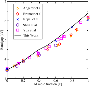
The bandgaps calculated using the above method for relaxed AlxGa1-xN (Figure 1) are seen to match quite closely with several reported experimental results. This provides validation for our cubic interpolation methodology.
Now, for strained AlxGa1-xN, the on-site energies may be assumed to remain unchanged since they correspond to the atomic energies, while the the coupling parameters from Table 1 are modified per Harrison’s ruleHarrison :
| (2) |
() being the strained (unstrained) lattice constant. Our calculations are meant for typical device applications where the AlxGa1-xN film thicknesses would be less than 25nm, implying pseudomorphic AlxGa1-xNGoyal2013 wherein the strain is given by:
| (3) |
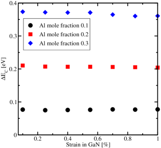
We point out that uniform scaling of the bond lengths and coupling parameters may be expected to lead to an overestimation of the effect of strain. This is because there is a compression along the c-axis for biaxial tensile strain in the basal hexagonal plane. However, the former is only about a fifth of the latter, due to a Poisson ratio of about 0.2 Lee . Further, the results of the following band offset calculations indicate that our assumption - of all the bond lengths scaling like the sides of the hexogonal base - do not make a material difference. In this work, band offsets have been defined as the difference between the conduction band edges of strained AlxGa1-xN and strained GaN. We have first estimated the bandgaps from the bandstructure. A fraction thereof, viz. 0.63 Ambacher , then gives the conduction band offset; this fraction was calibrated to match the experimentally reported 2DEG density Gordon using the calculation to be described in the following section. Figure 2 shows that while the band offset varies significantly with the Al mole fraction as expected, it changes only slightly as a function of the strain in the GaN layer. This is because, when the GaN is tensile strained, the conduction band minima of AlxGa1-xN shifts nearly as much as that of the GaN. We note that the relative insensitivity of the band offsets to GaN-layer strain renders our prior overestimation harmless. In the following section, we proceed to perform simulations based on the obtained results in order to estimate the 2DEG density.
III CHARGE-DENSITY SIMULATION
In order to study the impact of the GaN substrate strain on the 2DEG density at the AlxGa1-xN/GaN hetero-interface, we make use of the TCAD software package SILVACOSilv . Our approach involves calculation of the polarization charge in the heterostructure, followed by self-consistent solution of the one-dimensional Schrödinger and Poisson equations along the growth direction. The total polarization charge () at the AlxGa1-xN/GaN hetero-interface is obtained from the expression:
| (4) |
Here, () denotes the spontaneous (piezoelectric) polarization charges which is obtained from empirical expressions given by Ambacher et al. Ambacher . Thereafter, we follow a procedure due to Gordon et al. Gordon to obtain the self-consistent barrier height and 2DEG density . Here, the charge density transferred out of the surface donor states is calculated as:
| (5) |
where is the estimated surface barrier height, and is the constant surface donor density (cm-2eV-1) below the surface donor level (eV). Iteratively with this, the SILVACO Schrödinger-Poisson solver is used to calculate the 2DEG density n2DEG for a given . The latter is varied until the condition n is satisfied. At this point, and n. Note that we have considered a uniform distribution of the surface donor states Gordon ; Goyal2012 . Our results are observed to match well with the experimental data as given in Gordon et al. Gordon .
In the next step, we introduce strain in the GaN layer. This will introduce an additional piezoelectric polarization charge in the GaN layer itself. Further, it necessitates a recalculatation of the piezoelectric polarization charge term in AlGaN layer. The total polarization charge is thus modified as:
| (6) |
Where
| (7) |
| (8) |
Here, denotes the bulk lattice constant, () is the elastic constant, and () is the piezoelectric constant. The strained GaN lattice parameter is: with as the process-induced strain in the GaN layer. Indeed, the strain in the underlying GaN layer would not influence AlGaN surface state parameters. The basic bandstructure parameters for the strained GaN (namely electron affinity and bandgap) and its band offsets with the pseudomorphic AlxGa1-xN were taken from the bandstructure calculation described earlier and provided as inputs to the simulator through its C-Interpreter interface. Thereby, we can obtain the 2DEG density for different Aluminum mole fraction and GaN layer strain.
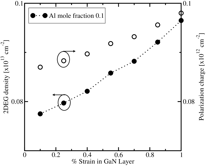
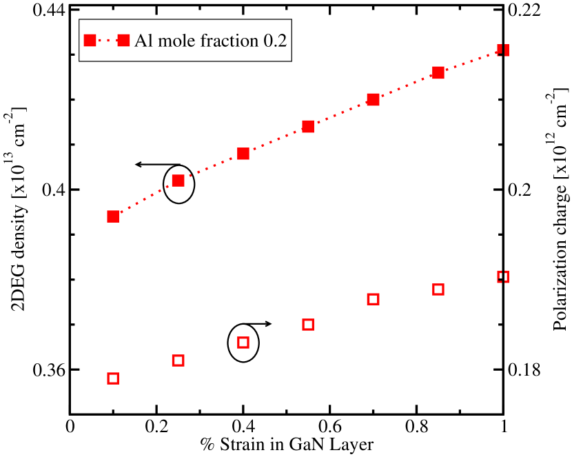
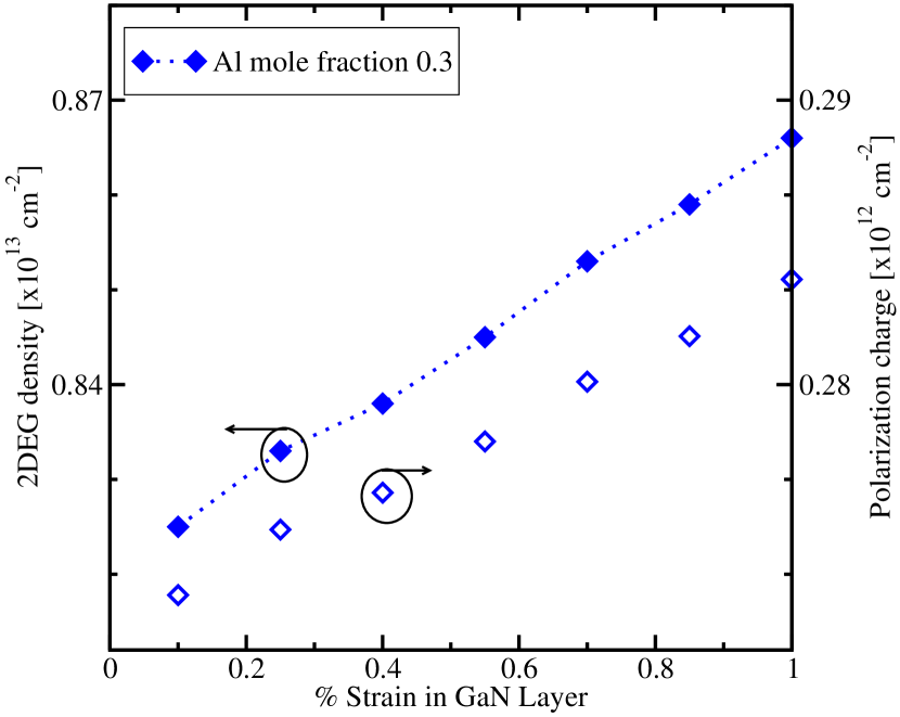
Figure 3 shows the simulated 2DEG density as a function of strain in the GaN substrate. The Al mole fraction is used as a parameter, and the AlGaN barrier thickness is set to 10nm. We find that the 2DEG density increases modestly with the strain in the GaN layer for a given . By following Equation 6 to Equation 8, we hypothesize that the strain in the GaN layer modulates the strain in the AlGaN layer, and thence the piezoelectric polarization therein. Figure 3 also shows the variation of polarization charge with strain. We find that the increase in in the AlGaN/GaN hetero-interface more or less tracks that of the 2DEG density, and thereby, explains its origin.
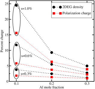
The percentage increase in the 2DEG density due to strain in GaN layer as a function of is shown in Figure 4. We have chosen three values of to show the impact of GaN layer strain on the 2DEG density. This impact is seen to decrease sharply with increasing . This happens because when increases, increases significantly: both the terms and are enhanced (c.f. Equation 6). Therefore, the impact of the incremental polarization charge due to strain in the GaN layer on will be marginalized. Our calculations predict maximal increase in the 2DEG at small , as much as 25% increase in the 2DEG density for =0.1.
IV CONCLUSION
The properties of AlxGa1-xN/GaN heterostructures have been computed for the case where the underlying GaN is tensile strained. Bandgaps and band offsets are calculated using the empirical tight-binding method, the polarization charge is calculated, and then a self-consistent Schrödinger-Poisson solver yields the 2DEG concentration at the hetero-interface. The strain in the GaN induces incremental strain in the AlGaN layer; this in turn leads to increased piezoelectric polarization. It is found that the band offsets have weak dependence on the GaN layer strain, because the latter induces roughly the same amounts of shift in the GaN and AlGaN conduction band edges. On the other hand, substantial enhancement in the 2DEG density is possible when the GaN layer is strained - this is due to the consequent increase in polarization. For larger Al mole fraction, the polarization is large anyway and the relative boost due to the GaN layer strain becomes smaller; therefore, the enhancement falls steeply with increasing Al mole fraction. Our work suggests that strain in the GaN layer - which might be unintentional today - could be used to achieve higher 2DEG density in the future if it can be engineered controllably. Lastly, it provides a framework to extend this effect to other III-N heterstructures.
References
- (1) O. Ambacher, J. Smart, J. R. Shealy, N. G. Weimann, K. Chu, M. Murphy, W. J. Schaff, and L. F. Eastman, R. Dimitrov, L. Wittmer, and M. Stutzmann, W. Rieger and J. Hilsenbeck, J. of Appl. Phys. 85:6, 3222 (1999).
- (2) J. P. Ibbetson, P. T. Fini, K. D. Ness, S. P. DenBaars, J. S. Speck, and U. K. Mishra, Appl. Phys. Lett. 77, 250 (2000).
- (3) A. Dadgar, J. Blaesing, A. Diez, A. Alam, M. H. and A. Krost, Jpn. J. Appl. Phys. 39, L1183 (2000).
- (4) M. Azize and T. Palacios, J. of Appl. Phys. 108, 023707 (2010).
- (5) H.-P. Lee, J. Perozek, L. D. Rosario and C. Bayram, Sci. Reports 6, 37588 (2016).
- (6) A. Kadir, C. C. Huang, K. E. K. Lee, E. A. Fitzgerald, and S. J. Chua, Appl. Phys. Lett. 105, 232113 (2014).
- (7) H. F. Liu, S. B. Dolmanan, T. N. Bhat, and S. Tripathy, Appl. Phys. Lett. 106, 176101 (2015).
- (8) L. Gordon, M-S. Miao, S. Chowdhury, M. Higashiwaki, U. K. Mishra, and C. G. Van de Walle, J. Phys. D:Appl. Phys. 43, 505501 (2010).
- (9) N. Goyal, B. Iniguez, and T. A. Fjeldly, Appl. Phys. Lett. 101, 103505 (2012).
- (10) N. Goyal, and T. A. Fjeldly, J. of Appl. Phys. 113, 014505 (2013).
- (11) J. Ghosh, A. Laha, D. Saha, and S. Ganguly, Proc. EUROSOI-ULIS, 156 (2017).
- (12) A. Kobayashi, O. F. Sankey, S. M. Volz, and J. D. Dow, Phys. Rev. B 28, 935, (1983).
- (13) J. C. Slater and G. F. Koster, Phys. Rev. 94, 1498 (1954).
- (14) C. T. Coughlan, PhD Thesis, University College Cork (2016).
- (15) H. H. Gürel, Ö. Akinci, H. Ünlü, Computational Materials Science 33:1-3, 269 (2005).
- (16) W. Shan, J. W. Ager, K. M. Yu, W. Walukiewicz, E. E. Haller, M. C. Martin, W. R. McKinney, and W. Yang, J. of Appl. Phys. 85, 8505 (1999).
- (17) D. Brunner, H. Angerer, E. Bustarret, F. Freudenberg, R. Höpler, R. Dimitrov, O. Ambacher, and M. Stutzmann, J. of Appl. Phys. 82, 5090 (1997).
- (18) N. Nepal, J. Li, M. L. Nakarmi, J. Y. Lin, and H. X. Jiang, Appl. Phys. Lett. 87, 242104 (2005).
- (19) H. Angerer, D. Brunner, F. Freudenberg, O. Ambacher, and M. Stutzmann, R. Höpler, T. Metzger, E. Born, G. Dollinger, A. Bergmaier, S. Karsch, and H.-J. Körner, Appl. Phys. Lett. 71, 1504 (1997).
- (20) F. Yun, M. A. Reshchikov, L. He, T. King, H. Morkoc, S. W. Novak, L. Wei, J. of Appl. Phys. 92:8, 4837 (2002).
- (21) W. A. Harrison, and S. Ciraci, Phys. Rev. B 10:4, 1516, (1974).
- (22) Atlas User’s Manual, https://www.silvaco.com.