Imaging Pulsed Laser Deposition oxide growth by in-situ Atomic Force Microscopy
Abstract
To visualize the topography of thin oxide films during growth, thereby enabling to study its growth behavior quasi real-time, we have designed and integrated an atomic force microscope (AFM) in a pulsed laser deposition (PLD) vacuum setup. The AFM scanner and PLD target are integrated in a single support frame, combined with a fast sample transfer method, such that in-situ microscopy can be utilized after subsequent deposition pulses. The in-situ microscope can be operated from room temperature (RT) up to 700∘C and at (process) pressures ranging from the vacuum base pressure of 10-6 mbar up to 1 mbar, typical PLD conditions for the growth of oxide films. The performance of this instrument is demonstrated by resolving unit cell height surface steps and surface topography under typical oxide PLD growth conditions.
I Introduction
A fascinating material class are the perovskite oxides due to their wealth in physical properties such as superconductivity, ferromagnetism, ferro- and dielectricity Eason (2009). Induced by the discovery of high- superconductors, pulsed laser deposition (PLD) has become a popular thin film growth technique to fabricate high quality oxide materials Bednorz and Muller (1986); Dijkkamp et al. (1987). The strength of depositing complex oxides with PLD comes from the fact that relative high oxygen pressures can be used while still having high kinetic energy ablated species, which strongly influences the films properties. Development of the current diagnostic tools such as high-pressure reflection high-energy electron diffraction (RHEED) Rijnders et al. (1997), surface x-ray diffraction (SXRD) Eres et al. (2002) and the more rarely used optical spectroscopic ellipsometry (SE), enabled to observe the oxide thin film growth. Using RHEED e.g., the growth mode and in some conditions the number of grown unit cells can be deduced by measuring the step density over time Neave et al. (1983); Shitara et al. (1992); Blank et al. (1999). The specular rod in SXRD descibes layer filling when the diffuse scattering contains information about the spatial distribution of islands, whereas with SE the evolution of the electronic structure can be monitor during film growth Blank and Rogalla (1997); Bijlsma et al. (1998). Although these scattering techniques are well established tools for monitoring the growth of oxides , the reciprocal information contained can be hard to interpret and they do not allow to probe growth properties of individual thin film islands as the surface reflectivity signal typically probes and averages over a surface area of millimeters in size. Besides this, diffraction techniques typically require crystalline surface planes to enable observation at all.
For microscopic real-space observations a popular diagnotic tool available are the scanning probe microscopes (SPM), enabling monitoring the surface topology at the (sub)nanometer spatial resolution Lippmaa et al. (1998, 2000); Iwaya et al. (2010); Shimizu et al. (2014). As most perovskite oxides are insulators or have a large band gap, application of scanning tunneling microscopy (STM) is rather limited as it is based on a tunneling current flowing between sample and tip Binnig et al. (1982); Sudheendra et al. (2007). Within the field of (PLD) oxide growth, microscopy analysis on surfaces is therefore typically done by post-deposition atomic force microscopy (AFM) or by ultra high vacuum (UHV) AFM. However, microscopically probing the surface during deposition is however a prerequisite in order to broaden our understanding of thin oxide film growth. Real space microscopy during film growth would give complementary information besides reciprocal techniques about microscopic events in thin film growth such as diffusion processes, ripening, defect formation etc. by measuring the nucleation density and individual thin film island evolution over time in between subsequent deposition pulses Rost et al. (2009), as in PLD deposition and growth are separated in time.
A first design and demonstration of a conventional AFM operating at metal-oxide PLD conditions has been reported Broekmaat et al. (2008); Broekmaat (2008), however the main drawback of typical AFM is the low sample throughput, as monitoring requires high-speed AFM instrumentation. Conventional AFMs are slow due to the low bandwidth of the cantilever, AFM scanner and electronics and optical detection signal. Recently, a lot of progress has been made to increase the bandwidth of these components in different enviroments, which shows the potential of high speed AFM in PLD conditions Rost et al. (2005); Kodera, Sakashita, and Ando (2006); Ando, Uchihashi, and Fukuma (2008); Schitter and Rost (2008); Ando (2012).
Here, we present the concept, specifications, design and performance of an atomic force microscope (AFM) in a pulsed laser deposition (PLD) vacuum setup. The setup consists of an in-situ AFM joined in an aluminum frame with an in geometrically position separated PLD position. Combined with a fast sample transfer system, this enables in-situ microscopy after subsequent deposition pulses. The AFM has been developed such that tapping mode (TM) and frequency modulated (FM) AFM can be applied at typical PLD conditions ranging from room temperature (RT) up to 700∘C and at (process) pressures ranging from the vacuum base pressure of 10-6 mbar up to 1 mbar. The performance of this instrument is demonstrated by resolving unit cell height steps of a SrTiO3(001) surface at PLD conditions as well as the evolution of the surface topography of a grown BiFeO3 film, a prototypical perovskite film. We conclude this paper with an outlook towards future applications as well as limitations of the current design.
II Concept
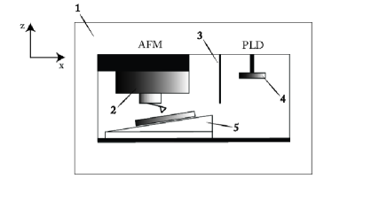
Fig. 1 shows a schematic illustration of a concept of AFM during PLD. In a support frame, an AFM scanner and PLD target are installed and a sample transfer stage is included. The AFM scanner is positioned geometrically separated from the PLD position for a main reason: It prevents blocking of deposition on the as-grown surface and unwanted AFM tip contamination. As deposition and growth in PLD are separated in time, growth can be studied in between subsequent pulses using this concept. A plasma screen between AFM and PLD should prevent any PLD plasma contamination on the AFM scanner.
In this concept, a sample is transferred back and forth between AFM and PLD, where the sample transfer is based on linear motion, see Fig. 1. A sample heater is mounted on top of a linear motion slider. The concept is such that the side approach Wessels et al. (2013) can be applied to reduce the time delay between PLD and AFM monitoring of the sample surface. The proposed configuration is straightforward to combine PLD with other diagnostics tools, such as scattering techniques as RHEED and plasma diagnostic tools for an increased understanding of thin film growth in PLD.
III Specifications
To image the surface topography at PLD conditions, the AFM has to be operated at pressures ranging from 10-6 mbar up to process pressures of 10-1 mbar. The applied gases typically involve (a mixture of) oxygen, argon and/or nitrogen.
The temperature window of typical growth conditions runs from room temperature (RT) up to about 700∘C, where the exact substrate temperature depends on the substrate material and ablated species.
AFM imaging, resolving the growth properties of individual thin film islands requires a stable AFM imaging at an image size of about 11m2 A short mechanical loop between the to be imaged substrate and AFM cantilever is required such that the noise levels, both, electronic and vibrational, should not exceed the substrate stepheight, typical 0.4 nm as typical oxide substrate steps are around 0.4 nm in height. This resolution is required both out-of-plane and in-plane.
To suppress thermal drift, an effective temperature stabilization is required. A thermal drift out-of-plane and in-plane, which enables measurement during 1 h would be required, as it is a typically duration involved in a PLD experiment. As we want to make use of image sizes of about 11 m2, this requires any in-plane drift to stay below 50 nm/min, thereby requiring minimal manual correction for imaging. The perpendicular thermal drift should stay within the piezo range to circumvent the requirement of a slow re-approach procedure.
To visualize the rapid growth processes involved, one needs to scan at high-speed, typically an image within seconds would be desirable, possibly even faster.
In order to reduce the dwell time between deposition and imaging, a fast sample transfer is required to minimize the time between geometrically seperated PLD position and AFM imaging. The repositioning error for subsequent back and forth motions has to stay below 100 nm.
The requirements can be summarized as follows:
-
•
Pressures during imaging: Ranging from 10-6 mbar (vacuum) up to 10-1 mbar in background gasses of (a mixture of) oxygen, argon and/or nitrogen.
-
•
Temperature range for imaging: RT up to 700∘C.
-
•
Imaging resolution: step resolution at oxide substrates (0.4 nm) at all mentioned pressure and temperature conditions.
-
•
Imaging rate: on the order of (tens of) seconds per image of 256256 pixels with images of about 11m2.
-
•
Thermal drift: below 700 nm/h in perpendicular direction, below 50 nm/min in-plane.
-
•
Transfer time before and after imaging: transfer time back and forth within 0.5 s with a repositioning error below 100 nm.
IV Design
In this section, the general architecture of the vacuum setup, the designed in-situ AFM within a PLD vacuum chamber and the design of the AFM scanhead is described in detail.
IV.1 Vacuum chamber and peripheral equipment
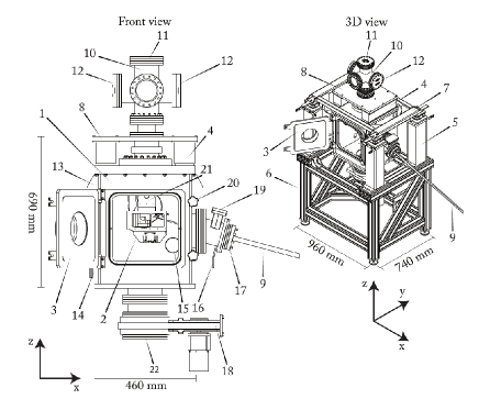
Fig. 2 shows a schematic representation of the designed PLD chamber and peripheral equipment. The PLD chamber is a single vacuum system, which differs in shape compared to traditional cylindrical chambers. In the designed vacuum system, the base pressure of 10-7 mbar is limited by O-rings of the vacuumdoor, valve on the flange on the laser beam path and the pressure controled valve. Typical PLD background pressures of 10-6 - 1 mbar are measured by almost closing this valve and varying the incoming gas flow between zero and 100 ml/min. The vacuumchamber is a square-like box design such that a vacuum chamber door is used to open up the system for accessibility to install the supporting frame for AFM and deposition. The vacuumdoor has a DN100CF flange viewport window, revolves by a shaft and can be closed by two closing knobs. Four airpod damping units together with matted corks placed underneath provide passive damping of system resonances validated by measuring the transfer function in x- and y-direction Segerink, Korterik, and Offerhaus (2011). The vacuum chamber houses an aluminum tube connecting the active damped system towards the supporting frame for AFM and deposition. The active damping stage is mounted as a lid on this PLD chamber ensuring good vibration isolation.
On top of the active damping stage, a five-way cross has been assembled providing feedtroughs for optical and electrical signals from and to the AFM scanner, coarse approach steppermotor, slider piezomotor drive and heater. The DN40CF flange ports are used for vacuum pressure gauges to measure both, process pressures as well as (high) vacuum pressures.
A KrF excimer laser beam aligned to an optical rail is integrated such that a 248 nm pulsed laser beam, having a typical pulse duration of 25 ns, is focused on the PLD target. As an entrance flange for the PLD excimer laser light, a flange is designed to enable the alignment of the laser onto the PLD target in an angle of 15∘ parallel to the targets surface. The flange is integrated with a valve to support laser intensity measurements behind the quartz window as well as a gasinlet for the applied background gasses. A flow meter controlled gas manifold has been designed to separately let (a mixture) of nitrogen, oxygen and/or argon into the vacuum chamber through this gas-inlet. At the bottom of the vacuum chamber, a DN200CF flange is connected to an adjustable valve typically used for automated pressure control followed by a turbomolecular pump.
IV.2 Support frame for microscopy and deposition
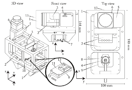
Fig. 3, schematically illustrates the supporting frame which contains the AFM and deposition stage. This aluminum frame, exhibiting a robust and high stiffness design, is attached by an aluminum tube to an active damping stage, see also Fig. 2. This damping stage has the functionality to lower the vibrational level in the mechanical loop of the AFM. The chosen shape and size of the support frame is based on required sizes and shape of the AFM scanner, PLD deposition and highest mechanical stiffness such that the required vibrational level is not exceeded. The aluminum frame consist of two assembled frames, where the top frame is used for integration of both the AFM scanner and PLD target. The -approach stage, containing a stepper motor having a step resolution of 100 nm/step, is positioned in the top frame to provide coarse approach towards the sample. A homebuilt mounting bracket connects the coarse approach stage to the AFM scanhead. The PLD target can be mounted onto a holder, adjustable in both height and lateral position along the sample transfer direction. In this design, the distance between the AFM tip and center of the PLD target is typically 50-60 mm, where the PLD target is shielded by a plasmascreen from the AFM scanhead.
The bottom frame has the functionality to integrate a sample transfer stage enabling back and forth sample transfer between the geometrically seperated AFM and deposition stage. A vacuum piezomotor with low vibrational level, a repositioning resolution within 20 nm and a maximum speed of 244 mm/s is installed in the bottom frame in order to propel the sample transfer stage which is designed to have minimal mass.
IV.3 AFM flexure scanner
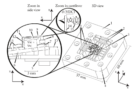
The AFM scanner is based on a flexure, see Fig. 4, which is often used in the field of high speed AFM Ando (2012). Flexure scanners are used as an alternative to commonly used low resonance frequency piezotubes to extend the mechanical scanner bandwidth several orders of magnitude into the kHz range Yong et al. (2012). In addition, stacked piezo’s integrated in a flexure results in less cross-coupling, hysteresis and creep as compared to generally used piezotubes. The AFM flexure in this work has been made out of Ti6Al4V to achieve high stiffness, a resulting high resonance frequency and low thermal expansion in order to minimize thermal drift. A simulation using finite element analysis resulted in a lowest resonance of 19 kHz for the flexure in the XY-plane. The maximum achievable linerate, estimated as 1/100th - 1/10th of the lowest resonance frequency Yong et al. (2012), is therefore between 0.19 - 1.9 kHz for this scanner design.
In order to achieve the desired scan range, we make use of piezo actuators with an expansion up to 4 m, which strongly reduces up to 1.4 m due to the high preload. The Z-flexure, a piezoring with an effective scan range of 1.4 m is aligned nearly in the center of the XY-flexure and can be positioned with high precision within the XY-plane by the double stacked XY-actuators. A counterbalance piezo, integrated in the Z-flexure, counters the momentum generated by center of mass movement of the Z-piezo. The unit, holding the AFM chip, is displaced by this Z-piezo such that the actual cantilever is excited, see the inset in Fig. 4.
The bottom part of this unit is screwed on top of the Z-flexure and is milled under an angle of 7∘. On top of this a flat plate with dither piezo stack is mounted. To detect the cantilevers deflection we make use of optical interferometry through the ZrO2 ferrule shown in Fig. 4 instead of the more common optical beam deflection method. Beam deflection requires use and adjustment of optical instrumentation, such as mirrors and is unpractical under PLD conditions, where space is lacking. Therefore, usage of interferometric detection results in a more compact design. A laser beam is reflected from the cantilever top side and fiber-air interface, where the cantilever and fiber are separated by 40-50 nm. A reference wave is reflected by the planar end of the fiber (glass-air interface). The detected wave is reflected by the top face of the cantilever. Both light waves interfere on a photodiode for detection. The optimal interference working point distance of the cavity can be adjusted by a DC voltage over the dither piezo. On top of this , an AC voltage (typically = 1 mV - 1 V) is applied to oscillate the cantilever at its resonance frequency in dynamic mode AFM.
V Performance
In this section we demonstrate the performance of the crucial components of the experimental setup. We focus here on the vibrational level and characteristics of the setup under PLD conditions. We then turn to the imaging performance by demonstrating the imaging of a typical oxide surface, SrTiO3(001), under some typical conditions experienced in a PLD experiment as well as the imaging of the growth of a BiFeO3 film under its PLD growth conditions.
V.1 Vibrational level and stage translation
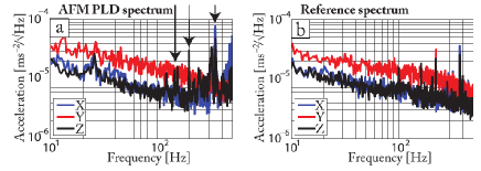
Fig. 5 shows the X,Y,Z acceleration levels of the AFM-PLD setup operating at 0.1 mbar oxygen background pressure in comparison to that of the acceleration levels of a commercial AFM setup (Bruker Dimension Icon) operating in ambient conditions. Both systems are placed on the same VC-G classified floor. The vibrational level sensors are positioned in the mechanical loop from tip to the sample, see Fig. 3. The passive damping system suppresses the higher frequencies 100 Hz, whereas the active damping stage significantly decreases acceleration levels from 10 - 100 Hz. Damping of the system by the airpods is mainly done in the Z-direction. There is no significant influence in acceleration levels observed for the peripheral equipment. Acceleration levels of the designed setup are similar to the commercial AFM setup, see Fig. 5. Only resonance frequencies of the aluminum support frame, see Fig. 2, are found at 140, 190 and several peaks between 300 - 400 Hz, marked by arrows in Fig. 5.
Crucial for the designed setup, is the performance (directly) after stage transfer. We therefore recorded the time domain signal together with the acceleration levels during such transfer. The vibrational decay time of the mechanical AFM tip-sample loop is determined from the time domain signal from the moment that the transfer stage velocity is zero at the AFM position after sample transfer from PLD position to the AFM position, for more details we refer to our earlier report Wessels et al. (2013). In the parallel acceleration level measurements, resonance peaks are observed at 140 and 280 Hz directly after stage deceleration and a corresponding delay time of 0.4 s. The back and forth sample transfer between AFM and PLD is possible in 0.5 s driving at maximum acceleration and velocity.
V.2 The role of PLD conditions
Typical PLD conditions involve substrates at elevated temperatures and process pressures up to several mbar, a pressure regime where cantilever response is known to alter dramatically Lübbe et al. (2011). The cantilever resonance frequency and the cantilever quality factor are nearly constant at pressures ranging from 10-6 - 0.1 mbar Mertens et al. (2003). However, increases from a few hundred to tens of thousands in the pressure regime 1 bar - 0.1 mbar Lübbe et al. (2011), corresponding to a broadening in its frequency response.
Also the elevated substrate temperatures involved in PLD growth, can result in temperature variations of the cantilever during stage transfer. These temperature variations are known to result in unwanted drift of the eigen frequency of the cantilever as the cantilevers dimensions alter and the Young’s modulus of silicon is known to vary reasonably upon temperature. Measuring at RT and within close vicinity of a sample heated up to 600∘C at a process pressure of 10-1 mbar resulted in a frequency shift of 200 Hz, corresponding to a temperature increase of the cantilever of 70 ∘C. By use of cantilevers with reasonable but rather low factors, the used side-approach Broekmaat et al. (2008) upon stage transfer can still be made succesfull, having the compromise of lower resolution. By the use of a radiation shield we prevented thermal radiation to influence the working point distance of the interferometric setup
V.3 AFM imaging
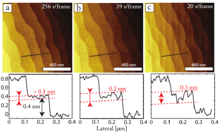
In order to demonstrate the scan speed performance we performed tapping mode (TM)-AFM measurements in air, shown in Fig. 6. The scan speed is increased for figures Fig. 6 (a-c) measuring the SrTiO3(001) substrate steps of 0.4 nm in height. At conventional AFM scan speeds, having a 2 Hz line rate (corresponding to an acquisition time of 256 s/frame), the subnanometer SrTiO3 substrate steps are clearly resolved, see also the height profiles in Fig. 6. From this line-profile, a peak-to-peak RMS of 0.1 nm was found. Upon reducing the acquisition time, see Fig. 6(b) and (c), towards respectively 39 s/frame and 20 s/frame, this peak-to-peak RMS increases towards 0.3 nm. In addition, a resonance frequency of 1.6 kHz is appearing, a vibrational mode of the mounting bracket connection with the coarse approach stage.
The increase in peak-to-peak z-noise can be attributed to two sources; firstly the electronic noise which increases proportional to , note that the used electronics are known to deliver sufficient resolution at video rate and beyond Rost et al. (2005). Secondly, the currently used photodetector which is limited to 400 kHz, thereby practically limiting to cantilevers of 300 kHz. A reduced pixel dwell time results in less oscillations used to determine a RMS value for every single pixel.
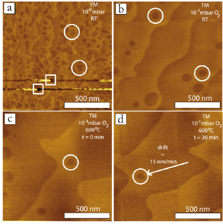
Typical PLD conditions involve process pressures ranging from high vacuum conditions up to 1 mbar. To demonstrate the use of the microscope at these conditions, in Fig. 7 we show AFM images recorded under typical PLD conditions. In Fig. 7(a), a frequency-modulated (FM) AFM image is depicted of a SrTiO3(001) substrate containing unit cell vacancy islands of 0.4 nm deep recorded in a background pressure of 10-6 mbar at RT Koster et al. (1998). In this pressure regime, the FM-AFM imaging mode is typically used due to the high for image stability reasons and lower transient time compared to TM-AFM Garcia and Perez (2002); Albrecht et al. (1991). In this FM-AFM image, the vertical resolution is similar to the z-noise level (0.1 nm) and unit cell (0.4 nm) deep vacancy islands are resolved having lateral sizes of 20 nm.
In Fig. 7(b), a TM-AFM image is depicted of a SrTiO3(001) substrate at 10-1 mbar oxygen background pressure , which is a typical PLD pressure to deposit perovskite oxide films ensuring good crystal quality, properties, stoichiometric transfer and 2D growth Groenen et al. (2015). At 10-1 mbar oxygen background pressure, the free cantilever amplitude was set to 120 nm and is found to be the most critical parameter for AFM imaging. The lateral AFM resolution on terraces is lowered as a SrTiO3(001) step broadening of 20 nm is found at this pressure. An average in-plane drift of 2 nm/min is measured over a period of 3.5 hours under these conditions.
The same AFM settings have been used for a sample measured at T=600∘C. At pressures of 10-1 mbar oxygen and sample temperatures of T=600∘C vacancy islands can easily be resolved. The AFM noise increase due to temperature is negligible based on the fact that z-noise level and SrTiO3(001) step broadening remained at T=600∘C Broekmaat (2008). Under these conditions, a drift of 15 nm/min is measured as depicted in Fig. 7. After hours of stable AFM imaging under oxide PLD conditions, the z-piezo stayed within range (700 nm).
V.4 AFM imaging during and after PLD
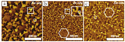
BiFeO3 has been deposited as a prototypical ABO3 film using the described PLD system. This material has multiferroic properties and its growth and property relation is intensively studied Lim et al. (2008); Béa et al. (2011); Kanashima et al. (2014); Deepak et al. (2015); Solmaz et al. (2016). It is reported that BiFeO3 tends to grow in several types of domains by modifying the SrTiO3(001) termination Solmaz et al. (2016). Dependent on the substrate termination, BiFeO3 grows either 1D/2D or 3D. Here, BiFeO3 films have been grown on TiO2 terminated SrTiO3(001) substrates anticipating 3D growth. BiFeO3 was deposited with a laser fluence of 2.0 J/cm2 , 0.3 mbar oxygen background pressure, a sample temperature of 600-670∘C during deposition and a repetition rate =0.5 Hz, all settings similar to previous work where only a target-substrate distance of 45 mm is used instead of 55 mm Solmaz et al. (2016). Fig. 8 shows AFM images obtained after and during BiFeO3 deposition. In Fig. 8(a), an ex-situ AFM image is depicted of a BiFeO3 film after deposition of 1000 pulses at 670∘C with a film thickness of 3-4 nm. This BiFeO3 film was deposited as a reference to reported literature Solmaz et al. (2016). It is reported that BiFeO3 grows 3D on TiO2 terminated SrTiO3(001), which is similar to the results obtained here. Terraces with on top 3D islands are visible after 1000 PLD pulses of BiFeO3 deposited on TiO2 terminated SrTiO3(001). The 3D BiFeO3 islands on top of the terraces suggest that next layer nucleation starts before a previous layer is completely covered. Island step heights are found of 0.2 nm, 0.4 nm and its multiples up to a maximum peak-to-peak height of 3 nm. Islands of 25-30 nm in lateral size are obtained on top of random shaped islands. From these results, it is expected that BiFeO3 growth will continue 3D, similar to what has been reported Solmaz et al. (2016).
In Fig. 8(b), an in-situ AFM image is presented, which was recorded at T=600∘C, as this is the maximum stable operating temperature for AFM measurements. The process pressure used was 0.3 mbar oxygen background pressure depositing again 1000 pulses of BiFeO3. The AFM image was taken after BiFeO3 deposition, sample transfer from PLD to AFM and an AFM stabilization time of 2h at the AFM position. After thermal stabilization, AFM was started with similar settings used for imaging of a SrTiO3(001) substrate. It became clear that due to an increase in surface roughness after deposition, the integral gain of AFM electronic feedback had to be increased significantly to visualize the smallest BiFeO3 islands. Stable AFM imaging was continued for several hours on BiFeO3 without thermally drifting out of the z-range. Thermal drift causes small distortions at AFM image edges. Smallest lateral BiFeO3 island sizes of 20-30 nm have been measured, similar to the results obtained with an ex-situ AFM on BiFeO3 after deposition at T=670∘C Solmaz et al. (2016). Some of these small islands are surrounded by a white circle marker in Fig. 8. In Fig. 8(b), the square white marker represents a zoom-in of a BiFeO3 taken from an 0.80.8 m2 AFM image.
Afterwards, the BiFeO3 film grown on SrTiO3(001) at T=600∘C had a cooldown of 15∘C/min in its deposition pressure of 0.3 mbar oxygen background pressure. Once the sample reached RT, it was exposed to a maximum oxygen flow up to atmospheric pressure. In Fig. 8(c), an ex-situ AFM image is depicted of BiFeO3 after oxygen exposure up to atmospheric pressure. The AFM image in Fig. 8(c) is slightly different compared to Fig. 8(b). One difference is that BiFeO3 islands of 20-30 nm are hardly visible in the ex-situ AFM image, see Fig. 8(c). Both AFM images have in common that BiFeO3 islands within polygon markers are similar in size. Note that, decreases more than an order of magnitude from 10-1 mbar background pressure up to atmospheric pressure.
This study reveals that BiFeO3 can be imaged using a Si AFM tip at T=600∘C and 0.3 mbar process pressure after deposition on a TiO2 terminated SrTiO3(001) substrate. Neck formation has not been observed using this tip-sample combination under these conditions. One of the ideas is to deposit BiFeO3 on mixed terminated SrTiO3(001) in order to study growth (front evolution) differences on both SrO and TiO2 termination. However, AFM imaging (Si tip) on mixed terminated SrTiO3 substrates results in neck formation at T=600∘C and 0.1 mbar process pressure, while stable AFM imaging was achieved on a TiO2 deposited film on TiO2 terminated SrTiO3(001) under the mentioned conditions. From the described measurements and the neck formation of a Si AFM tip with a SrRuO3 film (SrO termination) at T=600∘C and 0.1 mbar oxygen background pressure, it seems plausible to argue that a Si AFM tip forms a neck if the surface contains a SrO top layer Rijnders et al. (2004); Broekmaat (2008). For this tip-sample combination, another tip material/tip coating needs to be selected.
VI Conclusions and outlook
To visualize the topography of thin oxide films during growth, we have designed and integrated an atomic force microscope (AFM) in a pulsed laser deposition (PLD) vacuum setup. The in-situ microscope is demonstrated to operate at typical PLD conditions, thereby resolving unit cell height surface steps and surface topography.
We end this paper by discussing some aspects that might improve the performance of this microscope. The setup described here is a major step towards real-time AFM during PLD conditions. To enable quasi real-time AFM monitoring of island growth during PLD, the bandwidth of both the cantilever and (optical) detection system need to be improved, as the acquisition rate is currently limited by them. As high resonance cantilevers dictate smaller physical dimensions on the cantilever itself, the optical detection system might also need reconsideration. We are in the process of the development of self-sensing piezo-electric cantilevers in order to increase the bandwidth by (an) order(s) of magnitude.
Besides this, the thermal drift of the cantilever resulting from varying temperature gradients during sample transfer also needs reconsideration as slight temperature variations of the cantilever might result in a considerable eigenfrequency shift of it. Moreover, increasing both the AFM feedback bandwidth and transfer stage speed will result in a faster tip-sample approach time using the discussed side approach. We therefore currently develop a modification of the geometry such that the temperature of both sample and cantilever is better controlled together with a faster approach.
VII Acknowlegdement
This work is part of the research programme of NanoNext NL project 9A nanoinspectation and characterization, project 07 real-time atomic force microscopy growth monitoring during pulsed laser deposition of oxides.
VIII References
References
- Eason (2009) R. Eason, John Wiley and Sons, Hoboken, U.S.A. (2009).
- Bednorz and Muller (1986) J. Bednorz and K. Muller, Zeitschrift fuer Physik B Condensed Matter 64, 189 (1986).
- Dijkkamp et al. (1987) D. Dijkkamp, T. Venkatesan, X. D. Wu, S. A. Shaheen, N. Jisrawi, Y. H. Min-Lee, W. L. McLean, and M. C. P, Applied Physics Letters 51, 619 (1987).
- Rijnders et al. (1997) G. J. H. M. Rijnders, G. Koster, D. H. A. Blank, and H. Rogalla, Applied Physics Letters 70, 1888 (1997).
- Eres et al. (2002) G. Eres, J. Z. Tischler, M. Yoon, B. C. Larson, C. M. Rouleau, D. H. Lowndes, and P. Zschack, Applied Physics Letters 80, 3379 (2002).
- Neave et al. (1983) J. Neave, B. Joyce, P. Dobson, and N. Norton, Applied Physics A 31, 1 (1983).
- Shitara et al. (1992) T. Shitara, D. D. Vvedensky, M. R. Wilby, J. Zhang, J. H. Neave, and B. A. Joyce, Applied Physics Letters 60, 1504 (1992).
- Blank et al. (1999) D. Blank, G. Koster, G. Rijnders, E. van Setten, P. Slycke, and H. Rogalla, Applied Physics A 69, S17 (1999).
- Blank and Rogalla (1997) D. H. A. Blank and H. Rogalla, in Symposium II â In Situ Process Diagnostics and Intelligent Materials Processing, MRS Proceedings, Vol. 502 (1997).
- Bijlsma et al. (1998) M. E. Bijlsma, H. Wormeester, D. H. A. Blank, E. Span, A. v. Silfhout, and H. Rogalla, Phys. Rev. B 57, 13418 (1998).
- Lippmaa et al. (1998) M. Lippmaa, M. Kawasaki, A. Ohtomo, T. Sato, M. Iwatsuki, and H. Koinuma., Applied Surface Science 130, 582 (1998).
- Lippmaa et al. (2000) M. Lippmaa, N. Nakagawa, T. Kinoshita, T. Furumochi, M. Kawasaki, and H. Koinuma, Physica C Superconductivity 355, 196 (2000).
- Iwaya et al. (2010) K. Iwaya, T. Ohsawa, R. Shimizu, T. Hashizume, and T. Hitosugi, Applied Physics Express 3, 075701 (2010).
- Shimizu et al. (2014) R. Shimizu, T. Ohsawa, K. Iwaya, S. Shiraki, and T. Hitosugi, Crystal Growth & Design 14, 1555 (2014).
- Binnig et al. (1982) G. Binnig, H. Rohrer, C. Gerber, and E. Weibel, Physical Review Le 49, 57 (1982).
- Sudheendra et al. (2007) L. Sudheendra, V. Moshnyaga, E. D. Mishina, B. Damaschke, T. Rasing, and K. Samwer, Physical Review B 75, 172407 (2007).
- Rost et al. (2009) M. J. Rost, G. J. C. van Baarle, A. J. Katan, W. M. van Spengen, P. Schakel, W. A. van Loo, T. H. Oosterkamp, and J. W. M. Frenken, Asian Journal of Control 11, 110 (2009).
- Broekmaat et al. (2008) J. Broekmaat, A. Brinkman, D. H. A. Blank, and G. Rijnders, Applied Physics Letters 92, 043102 (2008).
- Broekmaat (2008) J. J. Broekmaat, In-situ growth monitoring with scanning force microscopy during pulsed laser deposition, Ph.D. thesis, Enschede (2008).
- Rost et al. (2005) M. J. Rost, L. Crama, P. Schakel, E. van Tol, G. B. E. M. van Velzen-Williams, C. F. Overgauw, H. ter Horst, H. Dekker, B. Okhuijsen, M. Seynen, A. Vijftigschild, P. Han, A. J. Katan, K. Schoots, R. Schumm, W. van Loo, T. H. Oosterkamp, and J. W. M. Frenken, Review of Scientific Instruments 76, 053710 (2005).
- Kodera, Sakashita, and Ando (2006) N. Kodera, M. Sakashita, and T. Ando, Review of Scientific Instruments 77, 083704 (2006).
- Ando, Uchihashi, and Fukuma (2008) T. Ando, T. Uchihashi, and T. Fukuma, Progress in Surface Science 83, 337 (2008).
- Schitter and Rost (2008) G. Schitter and M. J. Rost, Materials Today 11, 40 (2008).
- Ando (2012) T. Ando, Nanotechnology 23, 062001 (2012).
- Wessels et al. (2013) W. A. Wessels, J. J. Broekmaat, R. J. L. Beerends, G. Koster, and G. Rijnders, Review of Scientific Instruments 84, 123704 (2013).
- Segerink, Korterik, and Offerhaus (2011) F. B. Segerink, J. P. Korterik, and H. L. Offerhaus, Review of Scientific Instruments 82, 065111 (2011).
- Yong et al. (2012) Y. K. Yong, S. O. R. Moheimani, B. J. Kenton, and K. K. Leang, Review of Scientific Instruments 83, 121101 (2012).
- Lübbe et al. (2011) J. Lübbe, M. Temmen, H. Schnieder, and M. Reichling, Measurement Science and Technology 22, 055501 (2011).
- Mertens et al. (2003) J. Mertens, E. Finot, T. Thundat, A. Fabre, M.-H. Nadal, V. Eyraud, and E. Bourillot, Ultramicroscopy 97, 119 (2003).
- Koster et al. (1998) G. Koster, B. L. Kropman, G. J. H. M. Rijnders, D. H. A. Blank, and H. Rogalla, Applied Physics Letters 73, 2920 (1998).
- Garcia and Perez (2002) R. Garcia and R. Perez, Surface Science Reports 47, 197 (2002).
- Albrecht et al. (1991) T. R. Albrecht, P. Grütter, D. Horne, and D. Rugar, Journal of Applied Physics 69, 668 (1991).
- Groenen et al. (2015) R. Groenen, J. Smit, K. Orsel, A. Vailionis, B. Bastiaens, M. Huijben, K. Boller, G. Rijnders, and G. Koster, APL Materials 3, 070701 (2015).
- Lim et al. (2008) S. H. Lim, M. Murakami, J. H. Yang, S.-Y. Young, J. Hattrick-Simpers, M. Wuttig, L. G.Salamanca-Riba, and I. Takeuchi, Applied Physics Letters 92, 012918 (2008).
- Béa et al. (2011) H. Béa, B. Ziegler, M. Bibes, A. Barthélémy, and P. Paruch, Journal of Physics: Condensed Matter 23, 142201 (2011).
- Kanashima et al. (2014) T. Kanashima, J. M. Park, D. Ricinschi, and M. Okuyama, Ferroelectrics 466, 63 (2014).
- Deepak et al. (2015) N. Deepak, P. Carolan, L. Keeney, P. F. Zhang, M. E. Pemble, and R. W. Whatmore, Chemistry of Materials 27, 6508 (2015).
- Solmaz et al. (2016) A. Solmaz, M. Huijben, G. Koster, R. Egoavil, N. Gauquelin, G. V. Tendeloo, J. Verbeeck, B. Noheda, and G. Rijnders., Advanced Functional Materials 26, 2882 (2016).
- Rijnders et al. (2004) G. Rijnders, D. H. A. Blank, J. Choi, and C. B. Eom, Applied Physics Letters 84, 505 (2004).