Two-dimensional semimetal in HgTe quantum well under hydrostatic pressure
Abstract
We report results of systematic measurements of charge transport properties of the 20.5nm wide HgTe-based quantum well in perpendicular magnetic field, performed under hydrostatic pressures up to 15.1kbar. At ambient pressure transport is well described by the two-band semiclassical model. In contrast, at elevated pressure, we observed non-monotonic pressure dependence of resistivity at CNP. For pressures lower than kbar, resistivity grows with pressure, in accord with expectations from the band structure calculations and the model incorporating effects of disorder on transport in 2D semimetals with indirect band overlap. For higher pressures, the resistivity saturates and starts decreasing upon further increase of pressure. Above kbar the resistance and hopping transport character sharply change, which may indicate formation of the excitonic insulator state. The data also reveals strong influence of disorder on transport in 2D electron-hole system with a small band overlap.
I Introduction.
Two dimensional (2D) semimetals with coexisting electron and hole subsystems, attract considerable research interest due to a rich physics which is not fully understood. For a long time only one example of such system was known, the two-dimensional electron-hole system at the interface in GaSb-InAs-GaSb heterostructures Chang and Esaki (1980); Mendez et al. (1984, 1985); Washburn et al. (1985); Munekata et al. (1986); Washburn et al. (1986), where electrons and holes are spatially separated by an energy barrier. The discovery Kvon et al. (2008, 2011); Olshanetsky et al. (2012) of a new 2D e-h semimetallic system in HgTe quantum wells (QW) sparked interest to its studies and revived some long-standing problems in the physics of interacting low-dimensional systems as well as posed several new questions.
The HgTe QW becomes semimetallic when the thickness is greater than nm. The band overlap of about 1 meV Olshanetsky et al. (2012); Minkov et al. (2013) originates from the built-in strain due to the HgTe and CdTe lattice constant mismatch. The HgTe-based 2D semimetal is noticeably different from that for GaSb-InAs-GaSb in several important aspects: (1) it has much higher hole mobility and concentration, making the role of holes in transport much more pronounced; (2) electrons and holes are not spatially separated, therefore, one can expect more vivid manifestations of the electron-hole interactions; (3) the system is much more tunable by varying carrier concentrations in the gated structures, by engineering the QW width, and by tuning the energy spectrum with external pressure.
An old and famous problem in the physics of interacting electronic systems is the possibility of excitonic insulator (EI) formation. It is well known Halperin and Rice (1968) that semimetallic or semiconducting system should be unstable against exciton condensate formation, when band overlap or gap, EG, is lower than the exciton binding energy, EB. Significant complication comes from the strong influence of disorder on the EI formation. Since exciton is formed by oppositely charged particles, electrostatic potential of disorder produces the same effect on EI as magnetic impurity on superconductor: it lowers transition temperature and, for high enough concentration of impurities, suppresses pair condensation completely Zittartz (1967, 1968). As a result, only a few materials are considered suitable for observation of the EI state.
By now, several systems were suggested to exhibit the excitonic insulator state Neuenschwander and Wachter (1990); Brandt and Chudinov (1972); Du et al. (2015) In our previous work Olshanetsky et al. (2014), an attempt was made to realize this state in HgTe QW by tuning interaction with hydrostatic pressure. The idea behind the experiment was to diminish the indirect band overlap by applying pressure to the intrinsically strained heterostructure. Although in Ref. Olshanetsky et al., 2014 we observed an anticipated significant rise of resistivity under pressure of kbar at low temperature when the system was adjusted closely to the charge neutrality conditions (), a number of questions remained unaddressed.
The most important issue concerns evolution of the observed presumably EI state with pressure and the magneto-transport properties of the system. Recently, an alternative explanation of our results was suggested in Ref. Knap et al., 2014. This paper emphasized important role of disorder in transport properties of the 2D semimetals with a small band overlap. It was suggested, that in the presence of long-range disorder, the 2D semimetal with equal or nearly equal concentrations of electrons and holes should likely consist of spatially separated electron and hole puddles. Because of the indirect band overlap, the electron-hole scattering is mostly phonon-assisted and should freeze out at low enough temperatures. This should lead to a sharp increase of resistivity near the charge neutrality point when temperature decreases.
In this paper we report results of the extensive charge transport measurements for HgTe-based QW in perpendicular magnetic field, performed in the wide range of hydrostatic pressures, up to 15.1kbar. We significantly expanded the explored parameter space, as compared to Olshanetsky et al. (2014), and due to this, we traced the evolution of the transport with external pressure, temperature and magnetic field. Our current results suggest possible excitonic phase formation in high pressure range (>13 kbar) and also reveal strong influence of disorder on transport in 2D electron-hole system with a small band overlap.
II Experimental.
The CdxHg1-xTe/HgTe/ CdxHg1-xTe samples with 20.5nm wide HgTe-quantum well were grown by modified MBE technology on (100)-GaAs substrate. Details of the sample fabrication and structure design may be found elsewhere Dvoretsky et al. (2007); Olshanetsky et al. (2012); Kvon et al. (2008); Olshanetsky et al. (2009). The sample was lithographically defined as Hall bar in order to measure all components of the resistivity tensor. A TiAu film gate electrode deposited atop of the SiO2/Si3N4 gate insulator layer, enabled us to vary the density of holes and electrons in the QW in the range cm-2, at the rate cm.
Resistivity was measured by conventional four probe AC Lock-in technique. The current modulation frequency and amplitude were chosen in the range 5-20 Hz and 1-10 nA, correspondingly. The low currents ensured the absence of the electron overheating. Hydrostatic pressure was applied to the samples placed inside a BeCu cell of the piston-cylinder type with PES-1 as a pressure transmitting medium Kirichenko et al. (2005). All pressures were generated and clamped at room temperature. Then the pressure cell was cooled down to liquid helium temperatures. Pressure values cited below were determined from the superconducting transition of a tin gauge and refer to the low temperature conditions. The plate-like samples were oriented with 2D layer normal to the magnetic field direction. All magnetoresistance data presented below for diagonal and off-diagonal components of magnetoresistivity (magnetoconductivity) tensor, was symmetrized and antisymmetrized correspondingly by taking measurements in both magnetic field directions.
III Results and Discussion.
III.1 Zero magnetic field resistivity.
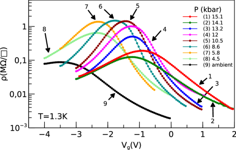
Figure 1 summarizes pressure evolution of the characteristics, measured at zero magnetic field and at K. Each curve was obtained by varying gate voltage at fixed temperature and pressure. For a fixed pressure, the maximal resistivity is achieved when the concentrations of electrons and holes are nearly equal; this is called ‘‘charge neutrality point’’ (CNP). The maximum is caused by two factors: when the system is close to CNP, concentrations of charge carriers are low. In addition, electron and hole scattering is stronger, because of the increased screening length. This type of dependence is well known and typical for 2D semimetallic system under considerationOlshanetsky et al. (2009); Kvon et al. (2011); Olshanetsky et al. (2012); Gusev et al. (2012).
In principle, one could determine more precisely the actual position of CNP from electron and hole concentration dependence on gate voltage, but in our case this was not possible for the reasons given below in the subsection ‘‘Magnetoresistance measurements’’. For low enough temperatures, true CNP and point of maximal resistivity are very close to each other, their minor difference is insignificant for our purpose, and in what follows we will refer to a point of maximal resistivity as CNP with no additional comments.
As shown in our earlier work Olshanetsky et al. (2014) the main difference in the characteristics under ambient and elevated pressure is that the resistivity near CNP sharply increases with pressure. New data reported here, indeed, confirms this previous result. Here we extend our measurements to pressures up to 15.1 kbar in order to trace systematically changes in the sample behavior with applied pressure. Measurements were made at the following sequence of applied pressure values: 0 15.114.11213.210.5 8.65.84.5 0 kbar.
When pressure rises up to 8.6 kbar, sample resistivity also rises. This is the type of behavior one expects from the band structure calculations Krishtopenko et al. (2016), which predict decrease in the band overlap when pressure increases. Resistivity behavior for higher pressures, however, is quite unexpected: as pressure rises above 8.6 kbar, the resistivity saturates and starts decreasing (see Fig. 1), indicating significant deviation from the simple band structure model.
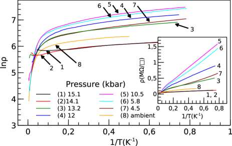
As was described in introduction, the most interesting physics is expected near CNP, therefore we measured temperature dependencies of resistivity at CNP for different pressure values. Figure 2 demonstrates vs dependencies for the same set of pressures as on Fig. 1. Gate voltage for each curve was set at the charge neutrality point and remained fixed during the temperature run.
The sheet resistance in Fig.2 typically exceeds 25 kOhm/ and one might anticipate a temperature activated or hopping type transport. This is indeed the case for high temperatures, K, however, for low temperatures the resistivity versus surprisingly slows down and follows law, rather than conventional hopping-type dependence Shklovskii and Efros (2013).
The slow temperature dependence is similar to that observed in a more narrow, 8–8.3 nm, HgTe quantum wells Gusev et al. (2013). In those structures saturation of the temperature dependence of resistivity at low temperatures was interpreted as a signature of edge transport. Although we didn’t explore other manifestations of edge-channel contribution to conductivity in our quantum wells, this explanation of the low temperature resistivity ‘‘slowing’’ seems plausible. We note, that the - type of the dependence was observed earlier Kvon et al. (2011) for semimetallic HgTe QW, grown on (112)-GaAs surface and remained unexplained. If one forces this dependence to fit temperature activated transport, , then the respective gap appears to be too small K to have a physical sense. For higher temperatures, K, (see the main panel in Fig.2) the versus is almost linear and is of the order of 100 K.
III.2 High temperature hopping transport
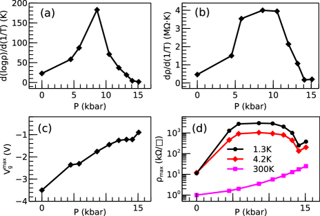
Interestingly, the slopes for both types of dependencies (at low and at high ) in appropriate coordinates and the value of resistivity at low temperatures as well, change with pressure in a non-monotonic manner. These changes are illustrated by Fig.3, which shows pressure dependencies of the slope, , maximum position () on ) characteristics, and resistivity at CNP (). Band structure calculations Krishtopenko et al. (2016) predict monotonic decrease of the band overlap with pressure. Correspondingly, one should expect a monotonic increase of resistivity at CNP with pressure. The observed nonmonotonic dependencies fall out of this semiclassical picture and we believe it results from the interplay of the band overlap and disorder, both parameters vary when pressure changes.
Pressure increase causes diminishing band overlap and, as a result, effective disorder becomes more important and leads to spatially inhomogeneous state. The inhomogeneous state may be viewed to consist of spatially separated conduction ‘‘lakes’’ and insulating ‘‘barriers’’; the activation energy in the temperature activated transport at high temperature therefore may be roughly related with a potential barrier height which the carriers need to overcome for hopping between the neighboring conduction lakes. In section III.3.3 further we will discuss the low-temperature ‘‘coherent’’ transport data which supports this conjecture of inhomogeneous state consisting of conduction lakes separated by potential barriers.
With this assumption, we conclude from Fig. 3a that the barrier height grows with pressure up to kbar. Upon further pressure increase, falls down to almost zero and tends to saturate, consistent with the power-low type dependence. The latter, in its turn, might indicate that the conduction areas start overlapping causing the barrier height to decrease. Finally, at 15 kbar the resistance sharply increases by a factor of 2-3 (see Fig. 3d). The latter increase might be caused by formation of EI; no such anomaly is seen at room temperature (see Fig. 3d, lower curve).
III.3 Magnetoresistance measurements
III.3.1 Overall behavior
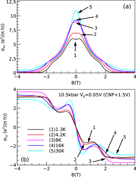
To gather more information on the origin of qualitative transformations of the charge transport with pressure, at each pressure point we performed a series of magnetoresistance (MR) measurements. The measurements were carried out for gate voltages ranging from -1.5 V to +1.5 V (relative to CNP), in the temperature interval from 1.3 to 30 K and in magnetic fields up to 4 T. The overall picture of magnetotransport looks more clear in terms of conductivity components, and , (rather than resistivity) which were obtained from resistivity tensor inversion. This will be further referred to as ‘‘magnetoconductivity’’(MC). We first consider the MC behavior at a particular representative pressure kbar.
The overall picture of МС at this pressure is shown on Fig. 4 for the lowest available temperature 1.3 K.
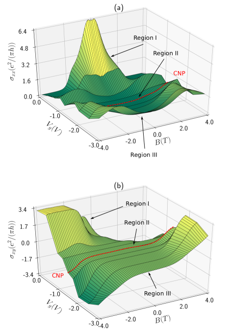
For the sake of convenience we divide the examined range of gate voltages into three regions as follows: (I) region of positive gate voltages relative to CNP, where electrons dominate in the charge transport, (II) region near CNP, and (III) region of negative voltages, where contribution to transport from holes is more significant than in region (I).
Region (I) is characterized by relatively high conductivity in low magnetic field and signatures of the developing quantum hall effect (QHE) in higher field (Fig. 5). The diagonal conductivity is negative for all magnetic fields, whereas off-diagonal exhibits emerging quantum Hall plateaus corresponding to filling factor. Figure 5 shows temperature evolution of the diagonal (panel (a)) and Hall (panel (b)) magnetoconductivity for the gate voltage V (i.e., +1.5 V relative to CNP). On Fig. 5 one can also see signatures of weak localization (WL) and weak antilocalization (WAL) in low fields T. They quickly vanish as increases above 1.3 K. (example of weak field MC fit with Hikami-Larkin-Nagaoka formula see on Fig. 13 in Appendix).
III.3.2 Smooth background semiclassical MC
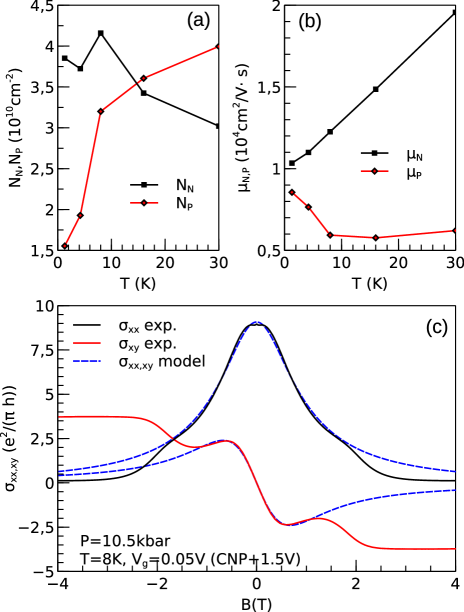
Besides quantum corrections, the MC has a smooth background, which persists throughout the examined temperature range in low magnetic fields (Fig. 5 a). Although the background MC presumably is of a semiclassical origin, temperature dependence of electron mobility, determined from the best fits of our data with two-band semiclassical model, contradicts the common sense arguments: the mobility grows with temperature, opposite to expectations based on usual scattering mechanisms. Would one attempts to explain these features by the CNP shift with temperature, the electron mobility would have dropped with temperature increasing. However, the fit with two-band model (for more detail, see Appendix) does not show such behavior of mobility and therefore this assumption does not make the two-band model relevant to our data. Moreover, the dependence also disagrees with the direct experimental data Olshanetsky et al. (2012). All these inconsistencies suggest that the two-band model, that successfully describes transport at ambient pressure Olshanetsky et al. (2012), is inadequate at high pressures.
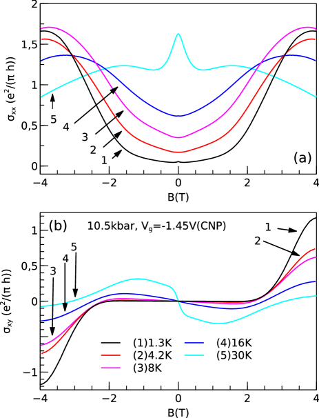
When we tune gate voltage close to CNP (region (II)), where concentrations of electrons and holes are equal (see Fig. 4), the overall picture changes drastically, as presented on Fig. 6. The diagonal conductivity falls down almost by an order of magnitude at K in comparison to that at , thus driving the system to the hopping conduction regime (see further for more detail). This regime corresponds to the wide ‘‘valley’’ of low conductivity in Fig. 4(a). The most striking is that the off-diagonal component of conductivity at low temperatures vanishes and remains zero in an extended range of fields (Fig. 4(b)). This effects persists in the interval of pressures from 4.5 to 12kbar and is missing at ambient pressure.
The zero Hall effect was observed earlier for a compensated electron-hole system in InAs/GaSb heterostructure Daly et al. (1996) in the quantum Hall effect regime. In that system, the zero Hall state emerges when the numbers of occupied electron and hole Landau levels are equal. This effect is concomitant of the strong peaks of between the quantized plateaus. The current situation is very different from the one observed in InAs/GaSb superlattice. In our case the low field magnetotransport is not determined by the energy spectrum quantization and certainly is of different origin. We believe that the low diagonal conductivity value, , is responsible for the seemingly unusual behavior of , which is simply a consequence of the fast growth of as temperature decreases.
III.3.3 Hopping transport features
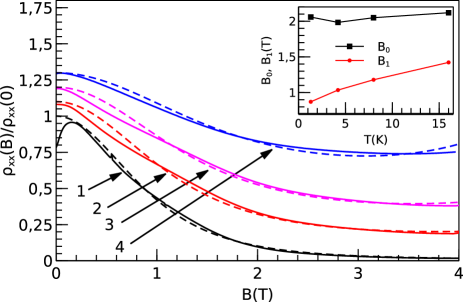
The second major feature of is that the low field magnetoconductivity in region II is positive (PMC), as opposed to that for region I; PMC persists up to, at least 16 K (Fig.6a). To understand this behavior we temporarily switch back from conductivity components to resistivity. The magnetoresistance data is shown on Fig. 7 by the solid lines. As one can see, resistivity here much exceeds 26k which is the upper limit for diffusive transport regime. Application of perpendicular magnetic field causes resistivity decrease by a factor of 50 at and . As temperature increases, the negative magnetoresistance gets smaller, but still is of the order of unity. For instance, changes by more than at K (Fig. 7).
The strong negative magnetoresistance is known to be intrinsic to the hopping conduction regime. A relatively simple model for negative MR of 2D disordered systems was proposed by Raikh and GlazmanRaikh and Glazman (1995). This model assumes carrier hopping between regions with delocalized states; it predicts quadratic fall of resistivity in low magnetic fields and exponential growth for higher fields. Such picture is feasible for 2D semimetal with small band overlap in the presence of impurity potential, as was pointed out in Knap et al. (2014), it was also observed for 2D electron system in the hopping regime Voiskovskii and Pudalov (1995) and seems applicable to our case. The analytical formula, describing resistivity behavior, with a number of simplifying assumptions is
| (1) |
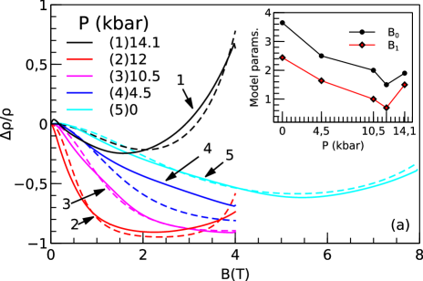
where B0 is connected to the parameters of potential barrier separating ‘‘lakes’’ of delocalized states, and B1 is related to geometry of the lakes being roughly inversely proportional to the average lake area. Fitting our data with this model and using two adjustable parameters is shown on Fig. 7 by dashed lines. One can see a satisfactory qualitative agreement of the model with experimental data.
Although in the original paper Raikh and Glazman (1995) the authors do not analyze temperature dependence of negative magnetoresistance, a brief comment is given there, that when the phase coherence length becomes comparable or shorter than the average lake size, one should expect the field dependence of resistivity to weaken. This is also in line with our observations. Temperature dependencies for the model parameters and , obtained from fitting, are shown on the insert to Fig.7. While is almost temperature independent, growth of indicates squeezing of the conducting lakes with temperature. The latter seems consistent with a simple picture of the lake, as a shallow potential well, where the number of bound carriers decreases as temperature becomes comparable with the confining potential.
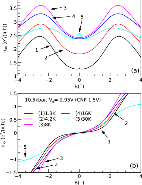
If one considers the negative (-1.5 V, relative to CNP) voltage biases (region(III)), the conductivity increases, but still corresponds to the hopping type transport. As well as in region II, the magnetoconductivity is well fitted with Glazman and Raikh model Raikh and Glazman (1995).
III.3.4 Weak antilocalization and puzzling MC in weak fields
In weak fields T and at the lowest temperatures, the narrow peak is observed both in the vicinity of CNP and far away of it, i.e. in regions I, II and III (see Figs. 5a, 6a, and 8a). Its width and magnitude correspond to the anticipated WAL; this effect was explored earlier Minkov et al. (2012) and is not discussed here. The WAL peak gradually disappears as temperature increases to 8K, which is also typical for the WAL effect.
Upon further increase in temperature above K, another, wider peak of negative magnetoconductivity emerges in low fields (see curve 5 in Figs. 5a, 6a, and 8a). The peak amplitude is much larger than that for the WAL and because of the high temperature it must be of a classical origin. This peak is accompanied with a sharp zig-zag change in the dependence, as can be seen on Figs. 5b, 6b, and 8b. The slope of the Hall conductivity at changes sign from positive to negative, indicating rise of electronic contribution to transport. Surprisingly, the peak amplitude grows as temperature increases from 16 to 30K.
This unusual behavior is qualitatively consistent with the predictions given in Ref. Knap et al., 2014 for temperature evolution of Hall conductivity for negative gate voltages. According to the theory, as temperature increases, the phonon-assisted electron-hole scattering grows and the electronic contribution to the transport becomes dominating because the electron mobility much exceeds that of holes. Physically, the conduction increases at high temperatures due to the increasing probability of carriers scattering between the electron and hole lakes, and transport obtains a conventional character typical for the two bands semiclassical transport regime. As magnetic field increases, the semiclassical two-band conduction produces negative magnetoconductivity; the interplay of these two factors shape the MC peak (curves 5 in Figs. 5a, 6a, and 8a). Upon further increase of field (e.g., above 0.5T on Fig. 6a) one can see a positive MR which may be interpreted as residues of the hopping-type NMR of the Raikh-Glazman type. >From the above considereation we conclude that at high temperatures two mechanisms, at least, contrbute to transport: (i) lake-to-lake hopping (with Raikh type negative MR), and (ii) electron-hole scattering leading to delocalization and diffusive transport.
To summarize this section, at a fixed pressure for high carrier concentrations (away of CNP), we observed developing of a conventional QHE regime with increasing magnetic field. For low carrier concentration, we see switching from semiclassical to hopping regime as temperature decreases from 30K to 1.3K. This behavior in some respects agrees with theoretical predictions, given in Ref. Knap et al., 2014, but some observed features don’t find explanation within the semiclassical framework.
III.3.5 Effect of pressure on magnetotransport.
Figure 9 shows how magnetotransport changes with pressure at CNP. Magnetoresistivity near CNP can be described by the model of Raikh and GlazmanRaikh and Glazman (1995) for all pressures. The corresponding model curves and dependencies of model parameters on pressure are shown on Fig. 9(a). As one can see, and decrease as pressure increases from zero to kbar. in other words, the electronic and hall lakes induced by the seeding disorder Knap et al. (2014) grow in size with pressure which may be interpreted as an effective delocalization. This behavior is consistent with the picture of the band overlap decrease with increase of pressure. The behavior of and for higher pressures (P kbar) sharply changes: both and start increasing thus indicating tendency to the disappearence of lakes and the barriers between them. Though the changes of and are not big, they produce an exponentially large impact on the resistivity. This agrees with sharp changes of the resistivity above 14 kbar (Fig. 3d). The sharp switching of the hopping transort characterstics above 14kbar may indicate formation of the EI state.
For pressures lower than 4.5 kbar, the low conductivity ‘‘valley’’ near CNP is almost absent supp . Magnetoconductivity here is consistent with the hopping transport model by Raikh and GlazmanRaikh and Glazman (1995).
Based on the observed evolution of magnetotransport we can conclude that (1) transport in a system near CNP corresponds to a hopping conductivity regime for pressures up to 14.1 kbar; (2) strong localization of carriers in this state seems to be driven by disorder, although the effect of electron-hole correlations can not be excluded; (3) transport properties near CNP strongly depend on the band overlap, tuned by application of pressure.
III.3.6 Irreversible effect of high pressure on the QW boundaries
After completion of the course of measurement on the way 15 kBar , when pressure was finally released, we observed an irreversible change of the sample resistivity in comparison to the initial value. This is shown on Fig. 10, where initial and final characteristics at ambient pressure and K are plotted.
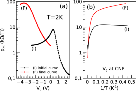
A detailed analysis of the data showed that the irreversible changes occurred right after application of the 15 kbar pressure, while further, as pressure was lowered, the sample properties changed quite reversibly.
To clarify the origin of the irreversible change in sample properties after pressure application cycle we made X-ray analysis of two samples: one exposed to high pressure and the pristine one. Rocking curve measurements revealed significant increase of dislocation density in QW after application of 15.1 kbar pressure. Therefore, the factor of ten increase in the sample resistivity after pressure release can be attributed to the generated dislocations. A concomitant effect of dislocation formation is the diffusion of Hg ions from the quantum well and barrier layers. The Hg ions are known to easily leave charged vacancies in a lattice. The structural changes impede disentangling the effects of disorder and lattice deformation on transport properties of the system. Nevertheless we made sure that behavior of the sample resistivity under pressure was quite reproducible, i.e. new defects were generated mainly at the initial loading of the cell. So we can attribute the reported changes of the sample resistivity with pressure to band structure changes rather than to changes in disorder. Strictly speaking, the disorder when compared with the band overlap, inevitably changes also with pressure, thus invoking both parameters to the problem.
IV Conclusion.
In summary, our experimental studies showed that application of pressure to a wide HgTe quantum well drastically alters its transport properties in comparison to ambient conditions. At ambient pressure transport is well described by the two-band semiclassical model. In contrast, at elevated pressure, we observed non-monotonic pressure dependence of resistivity at CNP. For pressures lower than kbar, resistivity grows with pressure, in accord with expectations from the band structure calculationsKrishtopenko et al. (2016) and the model incorporating effects of disorder on transport in 2D semimetals with indirect band overlapKnap et al. (2014).
For higher pressures, the resistivity saturates and starts decreasing upon further increase of pressure. Above pressure of kbar the resistance and hopping transport character sharply change, which may indicate formation of the EI state. Resistivity at CNP in the high temperature range follows the activated type temperature dependence, but its temperature changes weaken at low temperatures, where follows law. This can be compared to the temperature dependence of resistivity for 2D disordered semimetal, calculated in Ref. Knap et al., 2014. By redrawing it in logR-1/T and R-1/T coordinates, one can see that at low temperatures it is qualitatively very similar to our data: it saturates at low temperatures and demonstrates nearly linear shape in R-1/T coordinates. Nevertheless, calculated temperature dependence doesn’t show exponential growth at higher temperatures and do show saturation of R(1/T) dependence at low enough temperatures. The activation energy and the resistivity value itself change nonmonotonically with pressure, showing a maximum at kbar; we interpret this in terms of the pressure effect on the conductive lake size and insulating barriers between them. The resistivity at CNP and at negative gate voltages decrease dramatically with field at low B, followed by significant growth in higher magnetic field. This behavior is described reasonably well within the framework of Raikh and Glazman modelRaikh and Glazman (1995) of hopping conduction in the whole range of examined pressures. For temperatures above 16K we observe emergent conductivity peak and sharp sign change of the Hall conductivity in low magnetic fields, which may be explained as a result of the interplay of two different transport mechanisms, hopping and semiclassical two band diffusion.
As a side effect, we found that pressure also introduces defects in the crystal structure and revealed strong dependence of sample transport properties on disorder. Although we did not observe clear evidence of excitonic phase formation near CNP, a dielectric state, present at CNP is of quite unusual type and some of its unusual transport properties may be find explanation by taking the electron-hole interaction into account. We believe, further experimental research and development of appropriate theoretical models as well would be essential to understand the nature of possible electronic phases in disordered and interacting 2D semimetals.
V Acknowledgements
We thank S.S. Krishtopenko and V.P. Martovitsky for illuminating discussions. This work has been supported in part by RFBR Grant No. 16-32-00910. VMP acknowledges support by RSF 16-42-01100.
References
- Chang and Esaki (1980) L. Chang and L. Esaki, Surface Science 98, 70 (1980).
- Mendez et al. (1984) E. Mendez, L. Chang, C.-A. Chang, L. Alexander, and L. Esaki, Surface Science 142, 215 (1984).
- Mendez et al. (1985) E. Mendez, L. Esaki, and L. Chang, Physical review letters 55, 2216 (1985).
- Washburn et al. (1985) S. Washburn, R. A. Webb, E. Mendez, L. Chang, and L. Esaki, Physical Review B 31, 1198 (1985).
- Munekata et al. (1986) H. Munekata, E. Mendez, Y. Iye, and L. Esaki, Surface Science 174, 449 (1986).
- Washburn et al. (1986) S. Washburn, R. A. Webb, E. Mendez, L. Chang, and L. Esaki, Physical Review B 33, 8848 (1986).
- Kvon et al. (2008) Z. D. Kvon, E. Olshanetsky, D. A. Kozlov, N. N. Mikhailov, and S. A. Dvoretskii, JETP Letters 87, 502 (2008).
- Kvon et al. (2011) Z. Kvon, E. Olshanetsky, E. Novik, D. Kozlov, N. Mikhailov, I. Parm, and S. Dvoretsky, Physical Review B 83, 193304 (2011).
- Olshanetsky et al. (2012) E. Olshanetsky, Z. Kvon, N. Mikhailov, E. Novik, I. Parm, and S. Dvoretsky, Solid State Communications 152, 265 (2012).
- Minkov et al. (2013) G. M. Minkov, A. V. Germanenko, O. Rut, A. Sherstobitov, S. A. Dvoretski, and N. N. Mikhailov, Physical Review B 88, 155306 (2013).
- Halperin and Rice (1968) B. Halperin and T. Rice, Solid State Physics 21, 115 (1968).
- Zittartz (1967) J. Zittartz, Physical Review 164, 575 (1967).
- Zittartz (1968) J. Zittartz, Physical Review 165, 605 (1968).
- Neuenschwander and Wachter (1990) J. Neuenschwander and P. Wachter, PRB 41, 12693 (1990).
- Brandt and Chudinov (1972) N. Brandt and S. Chudinov, Journal of Low Temperature Physics 8, 339 (1972).
- Du et al. (2015) L. Du, W. Lou, K. Chang, G. Sullivan, and R.-R. Du, arXiv preprint arXiv:1508.04509 (2015).
- Olshanetsky et al. (2014) E. Olshanetsky, Z. D. Kvon, Y. A. Gerasimenko, V. Prudkoglyad, V. M. Pudalov, N. N. Mikhailov, and S. Dvoretsky, JETP Letters 98, 843 (2014).
- Knap et al. (2014) M. Knap, J. D. Sau, B. I. Halperin, and E. Demler, Physical review letters 113, 186801 (2014).
- Dvoretsky et al. (2007) S. Dvoretsky, D. Ikusov, D. K. Kvon, N. Mikhailov, N. Dai, R. Smirnov, Y. G. Sidorov, and V. Shvets, Optoelectronics, Instrumentation and Data Processing 43, 375 (2007).
- Olshanetsky et al. (2009) E. Olshanetsky, Z. Kvon, M. Entin, L. Magarill, N. Mikhailov, I. Parm, and S. Dvoretsky, JETP letters 89, 290 (2009).
- Kirichenko et al. (2005) A. Kirichenko, A. Kornilov, and V. Pudalov, Instruments and Experimental Techniques 48, 813 (2005).
- Gusev et al. (2012) G. Gusev, E. Olshanetsky, Z. Kvon, A. Levin, N. Mikhailov, and S. Dvoretsky, Physical review letters 108, 226804 (2012).
- Krishtopenko et al. (2016) S. Krishtopenko, I. Yahniuk, D. But, V. Gavrilenko, W. Knap, and F. Teppe, Physical Review B 94, 245402 (2016).
- Shklovskii and Efros (2013) B. I. Shklovskii and A. L. Efros, Electronic properties of doped semiconductors, Vol. 45 (Springer Science & Business Media, 2013).
- Gusev et al. (2013) G. Gusev, Z. Kvon, E. Olshanetsky, A. Levin, Y. Krupko, J. Portal, N. Mikhailov, and S. Dvoretsky, arXiv preprint arXiv:1308.4356 (2013).
- Daly et al. (1996) M. Daly, K. Dalton, M. Lakrimi, N. Mason, R. Nicholas, M. Van der Burgt, P. Walker, D. Maude, and J. Portal, Physical Review B 53, R10524 (1996).
- Raikh and Glazman (1995) M. Raikh and L. Glazman, Physical review letters 75, 128 (1995).
- (28) See Supplemental Material at [URL will be inserted by publisher] for more details on magnetoresistance evolution with pressure.
- Voiskovskii and Pudalov (1995) A. Voiskovskii and V. Pudalov, JETP Letters 62, 947 (1995).
- Minkov et al. (2012) G. Minkov, A. Germanenko, O. Rut, A. Sherstobitov, S. Dvoretski, and N. Mikhailov, Physical Review B 85, 235312 (2012).
*
Appendix A Modeling the magnetoconductivity for positive .
In this section we present a few additional pictures, which illustrate results of application of the two-band Drude model to the MC data for positive gate voltages.
Fitting procedure was as follows. In order to reduce the number of fitting parameters, at the first step, we determined the zero field slope of . Secondly, we determined the zero field conductivity by quadratic extrapolation of dependence in moderate fields (typically ) to zero. Direct determination of the Drude is rather difficult due to the presence of interference-induced corrections to conductivity at low temperatures and in low fields. Nevertheless, these contributions don’t affect the results in higher fields, may be reasonably excluded in weak field by parabolic extrapolation of the semiclassical fit to ; as will be shown further, both WAL and WL contributions may be then well fitted using the fitting parameters deduced at the first step. With these two quantities known, at the first step only two fitting parameters are left, i.e., electron and hole mobilities.
As one can see on Figs. 11(c) and 12(c) the model curves reproduce the low field behavior of both and with a reasonable set of parameters . The fit is successful for all pressures and temperatures as long as we consider positive gate voltages, far enough from CNP. Though there is some scattering of parameters (Fig. 12a), taken separately, each parameter has a feasible value for our system, but the whole set and temperature evolution of parameters appear to contradict expectations based on conventional models for transport in a 2D (semi) metallic systems. This can be clearly seen on Figs. 11 and 12 (a,b). Indeed, (i) the temperature dependencies of electron and hole concentrations and mobilities are opposite, (ii) the ratio of electron to hole mobility is unrealistically low. The electronic effective mass at ambient pressure was found to be an order of magnitude larger than that of the holesMinkov et al. (2013), therefore, one should expect much larger difference in the carrier mobility than the one, determined from our fitting parameters (see Fig. 12b). As was already mentioned in the main text, the small difference in mobilities also contradicts the results of earlier measurements with semimetallic HgTe QWs at ambient pressureOlshanetsky et al. (2012); Minkov et al. (2013).
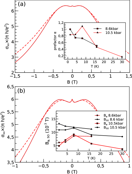
Despite low reliability of semiclassical parameters, they still can be used to calculate the WL and WAL corrections using conventional Hikami-Larkin-Nagaoka (HLN) formula:
A couple of examples of combined Drude and HLN fits is shown on Fig. 13. Corresponding model parameters as a function of temperature are shown on the inset on the same figure.
As one can see, the low field MC may be fitted with conventional WL model with a reasonable for our system set of parameters, but some of their temperature dependencies look rather scattered and, therefore, not very reliable. Taking into account a questionable validity of the semiclassical background, we expect to obtain not a quantitatively correct temperature dependence of the WAL parameters, but just their order of magnitude. As a result, we associate the region of positive gate voltages with semiclassical domain and relate the low field MC with WL-WAL corrections only at a qualitative level. More detailed analysis requires an adequate theory.