A Method for Building Low Loss Multi-Layer Wiring for Superconducting Microwave Devices
Abstract
Complex integrated circuits require multiple wiring layers. In complementary metal-oxide-semiconductor (CMOS) processing, these layers are robustly separated by amorphous dielectrics. These dielectrics would dominate energy loss in superconducting integrated circuits. Here we describe a procedure that capitalizes on the structural benefits of inter-layer dielectrics during fabrication and mitigates the added loss. We use deposited inter-layer dielectric throughout fabrication, then etch it away post-fabrication. This technique is compatible with foundry level processing and can be generalized to make many different forms of low-loss wiring. We use this technique to create freestanding aluminum vacuum gap crossovers (airbridges). We characterize the added capacitive loss of these airbridges by connecting ground planes over microwave frequency coplanar waveguide resonators and measuring resonator loss. We measure a low power resonator loss of per bridge, which is 100 times lower than dielectric supported bridges. We further characterize these airbridges as crossovers, control line jumpers, and as part of a coupling network in gmon and fluxmon qubits. We measure qubit characteristic lifetimes (’s) in excess of 30 s in gmon devices.
Two dimensional superconducting qubit architectures will require multi-layer wiring.Brecht et al. (2016); Harris et al. (2010); Lanting et al. (2014); Foxen et al. (2017); Rosenberg et al. (2017) Multiple wiring layers are fundamental to standard integrated circuits to route signals past one another to individually address a two dimensional grid of elements. Multi-layer wiring has been developed for superconducting circuits.Tolpygo et al. (2015); Nagasawa et al. (2014) These wiring layers are seperated by deposited dielectrics, and while these processes offer robust large scale control, the amorphous dielectrics used (typically SiO2) are quite lossy, with loss tangents .O’Connell et al. (2008); Quintana et al. (2014) We limit participation of similar dielectrics () to achieve state-of-the-art qubit quality factors ().Dunsworth et al. (2017); Dial et al. (2016) We have developed a method that benefits from the structural support of inter-layer dielectrics while mitigating the loss. We use deposited dielectrics only as a scaffold to separate and stabilize different metal layers through aggressive fabrication steps, and then etch it away at the end of fabrication. This process is compatible with standard CMOS processing, and provide an avenue toward scalable low-loss control wiring for a two dimensional grid of qubits. While this method is quite general and can be applied to many forms of multi-layer wiring we demonstrate this technique by fabricating the simplest forms of multi-layer wiring: crossovers.
Free standing metallic crossovers, known as airbridges, are widely used in low-loss microwave circuits Koster et al. (1989); Kwon et al. (2001) as well as superconducting circuits.Chen et al. (2014a); Abuwasib et al. (2013); Lankwarden et al. (2012) These airbridges are typically fabricated using re-flowed photoresist as a scaffold, which is removed immediately after bridge fabrication and prior to further processing. Released airbridges typically cannot withstand the sonication widely used to remove surface contaminants. Additionally, without dielectric support, the mechanical strength of freestanding airbridges relies on an arched shape. Airbridges with spans much larger than their arched height tend to bend under the pressure of resist spins and bakes. Thus, airbridges are made taller to span longer distances. Bridge height is limited by future processing, as standard high-resolution resists (-m thick) fail to protect taller airbridges from aggressive processing steps such as ion etching or lift-off. We use our dielectric scaffolding technique to create a different kind of airbridge. The dielectric scaffolding stabilizes these bridges through aggressive sonication and resist coating, thus decoupling the air bridges’ span from it’s height. Mechanical tests indicate these airbridges span distances of at least 70 m reliably. The added capacitive loss per bridge is comparable to photoresist scaffolded airbridges and is less lossy than conventional dielectric crossovers (bridges with the scaffolding left in-tact, as in Fig. 1).
We fabricate these airbridges after defining aluminum basewiring on high resistivity (10 kcm) intrinsic (100) plane silicon substrates. We optically pattern a tri-layer sup stack of resist as a lift-off mask and electron beam (e-beam) deposit 1 m of SiO2 to define our dielectric scaffold. Due to the growth conditions the SiO2 sidewalls form an approximately 45∘ with the substrate (see Fig. 1(b)). Next, we reapply the same lift-off process to define the bridge itself, except prior to deposition, we use an in-situ 400 V, 0.8 mA/cm2 argon ion mill to remove the exposed native aluminum oxide on the basewire. This mill allows DC electrical contact between base-wire aluminum and the 600 nm thick airbridge aluminum. After all further processing we use a dry VHF etcher (PRIMAXX ®VHF Etch Release Technology) to release the airbridges by removing the scaffolding SiO2. The chamber is pumped low vacuum, and the die is heated to 45 Celcius on a 3 inch silicon carrier wafer. A mixture of HF vapor, nitrogen, and ethanol is then bled into the chamber at a total pressure of 125 Torr (parameters in Table 1). The scaffold SiO2 and native oxide of the exposed silicon substrate are removed after 2 cycles of 15 seconds without breaking vacuum, as shown in Fig 1(c). Vapor phase release significantly reduces the mechanical strength required to overcome sticition, a common failure in microelectromechanical systems (MEMs) devices.Van Spengen et al. (2002); Maboudian and Howe (1997) This process does not attack other materials used in qubit fabrication including aluminum, aluminum oxide, and silicon.
| VHF Flow | N2 Flow | Ethanol Flow |
| (SCCM) | (SCCM) | (SCCM) |
| 190 | 1425 | 210 |
In our superconducting circuits these airbridges serve two main functions: ‘jumper airbridges’ which hop lines over each other and ‘ground plane airbridges’ which connect ground planes over lines. Jumper airbridges hop circuit elements over each other for stronger couplings, smaller footprints, and design flexibility. These SiO2 scaffolded airbridges can be made with contact pads as small as m2 and allow even micron width lines to hop over each other. Ground plane airbridges are commonly used to electrically connect ground planes to suppress parasitic microwave frequency slot line modes which modify couplings and act as qubit loss channels in coplanar waveguide (CPW) geometries.Ponchak et al. (2005); Houck et al. (2008) These airbridges also route return currents to reduce unwanted cross-talk between control lines.
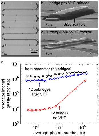
We measure the added capacitive loss from airbridges using CPW resonators. To measure resonator loss, we cool down chips in a heavily filteredBarends et al. (2011) adiabatic demagnetization refrigerator with a base temperature of 50 mK. We extract resonator internal quality factor (loss = ) by measuring and fitting the microwave scattering parameters versus frequency near resonance.Megrant et al. (2012) Each chip has ten resonators capacitively coupled ( between and ) to a common feedline. These resonators have between zero and ninety-eight groundplane airbridges spanning their center trace. The airbridges are 3 m wide and have a height above the center trace set by the original dielectric thickness of 1 m. In Fig. 1(a) we show one such resonator resonator spanned by 12 ground plane airbridges equally spaced along the resonator after the coupling arm. All resonators have a 10 m center trace and a 5 m gap to ground on either side, and resonance frequencies near 6 GHz.
We compare loss between three styles of resonators: resonators spanned by scaffolded bridges (Fig. 1(b)), resonators spanned by airbridges (after VHF release, Fig. 1(c)), and pureley CPW resonators with no crossovers of any kind (bare resonators). In Fig. 1(d) we display internal quality factor data for these three resonators. For clarity, we show only a single representative trace from each. The single photon loss limit approximately captures the physics of energy loss in superconducting qubits at the same frequency. The bare witness resonator has a low power internal quality factor of around which is consistent with single layer fabrication resonators of the same geometry. We saw little to no difference in bare resonator quality factors between chips with or without the VHF process. When the SiO2 is left intact, (as it would be in typical dielectric crossovers) the low power drops to around . This is consistent with an amorphous SiO2 loss tangent of and a participation of (roughly the added capacitance for twelve scaffolded bridges). After the VHF treatment, the of resonators with twelve airbridges recovers to a factor of 2 lower than the bare resonators. We measure the scaling of this residual loss with number of airbridges between zero and ninty-eight. The internal quality factor decreases with increasing number of airbridges and lines of best fit indicate added loss at low power of 3.9 per bridge.sup
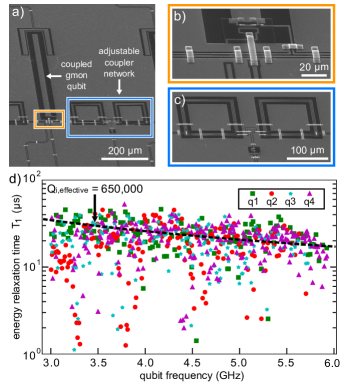
We use these low-loss airbridges as an integral part of gmon qubits. These qubits are transmon qubits Koch et al. (2007) with inductive taps placed between DC SQUID and ground plane to allow adjustable coupling to nearest neighbors.Chen et al. (2014b) It is critical that any added loss from the airbridges does not compromise the qubit coherence. In Fig. 2(a) we display one such gmon qubit with its neighboring coupler network. We bias these qubits’ DC SQUID loop with maximum DC current of 2 mA. This current flows entirely through a jumper crossover in-line with the flux bias line (Fig. 2(b)) and shows no evidence of on-chip heating. In the qubit circuit, we use many ground plane airbridges as well as a set of jumper airbridges in-line with the coupler’s geometric inductor (Fig. 2(c)). This jumper airbridge allows a gradiometric turn which further reduces crosstalk. These jumper airbridges are only 1.5 m wide, highlighting their small footprint. It is also important to note that these airbridges are fabricated prior to Josephson junction deposition, and are robust after all of the further processing, with yield limited by errors in lithography. In Fig. 2(d) we show qubit energy relaxation time () spectra over 3 GHz of tunable qubit frequency for four different qubits. The spectrum is well represented by a constant effective , with small sections where the drops dramatically. These spectra are consistent with qubit loss dominated by dielectric surface loss from the SQUID area.Dunsworth et al. (2017) The airbridges themselves do not appear to greatly impact the qubit spectra.sup
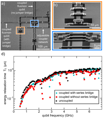
We also use these airbridges as integral parts of our fluxmonQuintana et al. (2017) flux qubit circuits, for both isolated and coupled qubits. The main inductance and capacitance of the fluxmon is distributed over a long CPW segment that is terminated with an electrical short to ground at one end and a DC SQUID shorted to ground at the other. We use both ground plane airbridges over the qubit’s CPW and jumper airbridges in-line with the qubit’s CPW and the couplers as well. We tested three variations of fluxmon qubits on the same chip: uncoupled, coupled with jumper bridge, and coupled without jumper bridge. The uncoupled qubits only use ground plane airbridges. For the coupled qubits, the CPW center trace of one qubit jumps over the CPW center trace of the other qubit via an airbridge, as shown in Fig. 3(a), while the other qubit does not have any in-line jumper airbridges.
The resulting qubit vs. frequency at symmetric bias (zero tilt bias) is shown in Fig. 3(d) for the three qubit variations. The background dissipation is believed to come from flux noise at low frequenciesQuintana et al. (2017); Yan et al. (2016) extrinsic to the airbridges, with some other inductive loss extrinsic to the airbridges dominating at high frequencies. We find no measurable difference in coherence between the two types of coupled qubits. This is consistent with a very high quality galvanic contact between the jumper bridge and the qubit’s CPW. Furthermore, we see no measurable difference in coherence between the coupled and uncoupled qubits, despite the fact that the coupled qubits are in very close proximity to a coupler circuit (the thin traces and ground plane pads in Fig. 3(c)) containing many crucial jumper and ground plane airbridges. This retained coherence is very important for scaling up fluxmon circuits with many jumper airbridges and couplers, in order to couple one qubit to many others at once for quantum annealing applications.
In summary, we have demonstrated a procedure that utilizes the structural benefits of inter-layer dielectrics commonly used in multi-layer wiring, while mitigating the capacitive loss. We use this process to fabricate low-loss airbridges that are robust during fabrication against strong sonication, other aggressive etches, and have a low profile. We measure the added loss per ground plane bridge over resonators to be at low power. We demonstrated these airbridges’ use in different superconducting qubit devices and measured little to no effect on the coherence of the qubits. These qubit designs fundamentally require a second layer of wiring, and here we have demonstrated a proof-of-principle method for rigidly scaffolding this second layer of wiring. Reapplication of the lift-off steps of SiO2 and metal (prior to VHF release) would allow for further layers of wiring as well as further complexity.sup By replacing the lift-off steps in the bridge fabrication with more standard blanket depositions and via etches, this technique is completely compatible with standard multi-layer CMOS processing.
I Acknowledgments
This work was supported by Google. C. Q. and Z.C. acknowledge support from the National Science Foundation Graduate Research Fellowship under Grant No. DGE- 1144085. Devices were made at the UC Santa Barbara Nanofabrication Facility, a part of the NSF funded National Nanotechnology Infrastructure Network.
References
- Brecht et al. (2016) T. Brecht, W. Pfaff, C. Wang, Y. Chu, L. Frunzio, M. H. Devoret, and R. J. Schoelkopf, npj Quantum Information 2, 16002 (2016).
- Harris et al. (2010) R. Harris, M. Johnson, T. Lanting, A. Berkley, J. Johansson, P. Bunyk, E. Tolkacheva, E. Ladizinsky, N. Ladizinsky, T. Oh, et al., Physical Review B 82, 024511 (2010).
- Lanting et al. (2014) T. Lanting, A. Przybysz, A. Y. Smirnov, F. M. Spedalieri, M. H. Amin, A. J. Berkley, R. Harris, F. Altomare, S. Boixo, P. Bunyk, et al., Physical Review X 4, 021041 (2014).
- Foxen et al. (2017) B. Foxen, J. Mutus, E. Lucero, R. Graff, A. Megrant, Y. Chen, C. Quintana, B. Burkett, J. Kelly, E. Jeffrey, et al., arXiv preprint arXiv:1708.04270 (2017).
- Rosenberg et al. (2017) D. Rosenberg, D. Kim, R. Das, D. Yost, S. Gustavsson, D. Hover, P. Krantz, A. Melville, L. Racz, G. Samach, et al., arXiv preprint arXiv:1706.04116 (2017).
- Tolpygo et al. (2015) S. K. Tolpygo, V. Bolkhovsky, T. J. Weir, L. M. Johnson, M. A. Gouker, and W. D. Oliver, IEEE Transactions on Applied Superconductivity 25, 1 (2015).
- Nagasawa et al. (2014) S. Nagasawa, K. Hinode, T. Satoh, M. Hidaka, H. Akaike, A. Fujimaki, N. Yoshikawa, K. Takagi, and N. Takagi, IEICE Transactions on Electronics 97, 132 (2014).
- O’Connell et al. (2008) A. D. O’Connell, M. Ansmann, R. C. Bialczak, M. Hofheinz, N. Katz, E. Lucero, C. McKenney, M. Neeley, H. Wang, E. M. Weig, et al., Applied Physics Letters 92, 112903 (2008).
- Quintana et al. (2014) C. Quintana, A. Megrant, Z. Chen, A. Dunsworth, B. Chiaro, R. Barends, B. Campbell, Y. Chen, I.-C. Hoi, E. Jeffrey, et al., Applied Physics Letters 105, 062601 (2014).
- Dunsworth et al. (2017) A. Dunsworth, A. Megrant, C. Quintana, Z. Chen, R. Barends, B. Burkett, B. Foxen, Y. Chen, B. Chiaro, A. Fowler, et al., arXiv preprint arXiv:1706.00879 (2017).
- Dial et al. (2016) O. Dial, D. T. McClure, S. Poletto, G. Keefe, M. B. Rothwell, J. M. Gambetta, D. W. Abraham, J. M. Chow, and M. Steffen, Superconductor Science and Technology 29, 044001 (2016).
- Koster et al. (1989) N. Koster, S. Koblowski, R. Bertenburg, S. Heinen, and I. Wolff, in Microwave Conference, 1989. 19th European (IEEE, 1989), pp. 666–671.
- Kwon et al. (2001) Y. Kwon, H.-T. Kim, J.-H. Park, and Y.-K. Kim, IEEE microwave and wireless components letters 11, 59 (2001).
- Chen et al. (2014a) Z. Chen, A. Megrant, J. Kelly, R. Barends, J. Bochmann, Y. Chen, B. Chiaro, A. Dunsworth, E. Jeffrey, J. Mutus, et al., Applied Physics Letters 104, 052602 (2014a).
- Abuwasib et al. (2013) M. Abuwasib, P. Krantz, and P. Delsing, Journal of Vacuum Science & Technology B, Nanotechnology and Microelectronics: Materials, Processing, Measurement, and Phenomena 31, 031601 (2013).
- Lankwarden et al. (2012) Y. Lankwarden, A. Endo, J. Baselmans, and M. Bruijn, Journal of Low Temperature Physics 167, 367 (2012).
- (17) See supplementary material.
- Van Spengen et al. (2002) W. M. Van Spengen, R. Puers, and I. De Wolf, Journal of micromechanics and microengineering 12, 702 (2002).
- Maboudian and Howe (1997) R. Maboudian and R. T. Howe, Journal of Vacuum Science & Technology B: Microelectronics and Nanometer Structures Processing, Measurement, and Phenomena 15, 1 (1997).
- Ponchak et al. (2005) G. E. Ponchak, J. Papapolymerou, and M. M. Tentzeris, IEEE transactions on microwave theory and techniques 53, 713 (2005).
- Houck et al. (2008) A. Houck, J. Schreier, B. Johnson, J. Chow, J. Koch, J. Gambetta, D. Schuster, L. Frunzio, M. Devoret, S. Girvin, et al., Physical review letters 101, 080502 (2008).
- Barends et al. (2011) R. Barends, J. Wenner, M. Lenander, Y. Chen, R. C. Bialczak, J. Kelly, E. Lucero, P. O’Malley, M. Mariantoni, D. Sank, et al., Applied Physics Letters 99, 113507 (2011).
- Megrant et al. (2012) A. Megrant, C. Neill, R. Barends, B. Chiaro, Y. Chen, L. Feigl, J. Kelly, E. Lucero, M. Mariantoni, P. O’Malley, et al., Applied Physics Letters 100, 113510 (2012).
- Koch et al. (2007) J. Koch, M. Y. Terri, J. Gambetta, A. A. Houck, D. Schuster, J. Majer, A. Blais, M. H. Devoret, S. M. Girvin, and R. J. Schoelkopf, Physical Review A 76, 042319 (2007).
- Chen et al. (2014b) Y. Chen, C. Neill, P. Roushan, N. Leung, M. Fang, R. Barends, J. Kelly, B. Campbell, Z. Chen, B. Chiaro, et al., Physical review letters 113, 220502 (2014b).
- Quintana et al. (2017) C. Quintana, Y. Chen, D. Sank, A. Petukhov, T. White, D. Kafri, B. Chiaro, A. Megrant, R. Barends, B. Campbell, et al., Physical Review Letters 118, 057702 (2017).
- Yan et al. (2016) F. Yan, S. Gustavsson, A. Kamal, J. Birenbaum, A. P. Sears, D. Hover, T. J. Gudmundsen, D. Rosenberg, G. Samach, S. Weber, et al., Nature communications 7, 12964 (2016).