Tunable plasmonic nanoantennas in rolled-up microtubes coupled to integrated quantum wells
Abstract
We propose and realize a tunable plasmonic nanoantenna design consisting of two stacked Ag cuboids that are integrated into a rolled-up semiconductor microtube. The antenna’s resonance is tuned by varying the cuboid’s distance to match the photoluminescence emission of an embedded GaAs quantum well. Spatially, spectrally and temporally resolved photoluminescence measurements reveal a redshift and a reduction in lifetime of the quantum-well emission as signatures for the coupling to the antenna system. By means of finite-element electromagnetic simulations we assign the coupling to an excitation of a high-order plasmonic mode inside the Ag cuboids.
keywords:
microtubes, silver cuboids, localized surface plasmons, high-order plasmonic mode, spectral shift, GaAs quantum wellsChemie] Institute of Physical Chemistry, University of Hamburg, Grindelallee 117, 20146 Hamburg, Germany \alsoaffiliation[Physik] Institute of Nanostructure and Solid State Physics, University of Hamburg, Jungiusstrasse 11, 20355 Hamburg, Germany Chemie] Institute of Physical Chemistry, University of Hamburg, Grindelallee 117, 20146 Hamburg, Germany Physik] Institute of Nanostructure and Solid State Physics, University of Hamburg, Jungiusstrasse 11, 20355 Hamburg, Germany Physik] Institute of Nanostructure and Solid State Physics, University of Hamburg, Jungiusstrasse 11, 20355 Hamburg, Germany Chemie] Institute of Physical Chemistry, University of Hamburg, Grindelallee 117, 20146 Hamburg, Germany
![[Uncaptioned image]](/html/1712.01162/assets/x1.png)
Noble metal nanostructures allow to control and manipulate light-matter interactions in the sub-wavelength regime 1, 2, 3. Their unique optical properties are governed by localized surface plasmons (LSPs), collective charge-carrier oscillations which are accompanied by both strongly confined electromagnetic fields and large field intensities. The capability of metal nanostructures to support LSPs has been exploited to remarkably modify light-emission properties of emitters such as increasing their fluorescence intensity 4, 5, 6, 7, 8, 9, 10, 11, altering their radiative and non-radiative decay rates 6, 11, 12, 13, 14 or reshaping their emission spectra 15, 16, 17. In this regard, the nanostructures are considered as plasmonic nanoantennas and the coupling to a close-by emitter is inherently dependent on the antennas’ composition, size, and geometry. Correspondingly, a manifold of antenna designs has been described including bow-tie 18, 9 and Yagi-Uda antennas19, 20, metallic nanorods 7, 21 and particle dimers 22, 13, 10. The variety of designs allows to reach a wide spectral range of LSP resonances but essentially requires a pinpoint control over the antenna’s geometry and a close distance of nanoantenna and emitter.
In this Letter, we propose and demonstrate the fabrication of a novel nanoantenna consisting of stacked Ag cuboids that are integrated into a rolled-up semiconductor microtube. The semiconductor compound includes a GaAs quantum-well (QW) heterostructure and thus the nanoantenna is directly placed adjacent to a robust quantum emitter. Microtubes with a functional metal layer have been previously exploited to realize rolling-up metamaterials 23, 24, 25, 26 and LSP-coupled whispering-gallery-mode resonators 27, 28. Here, we combine the defined rolled-up mechanism with a precise electron beam lithography approach to stack individual Ag cuboids into the wall of the micron-sized tube. By design, the distance of the Ag cuboids is varied and allows to tune the nanoantenna’s LSP resonance to match the photoluminescence (PL) emission energy of the embedded GaAs QW. We show by means of spatially and temporally resolved PL spectroscopy that the coupling of the GaAs QW emission to the plasmonic nanoantenna system is dependent on the lateral distance of the individual cuboids. For a distance of , we observe a redshift of the QW PL emission that is accompanied by a decrease in lifetime at the red-shifted spectral position. By means of finite-element electromagnetic simulations we attribute the spectral shift to an excitation of a high-order plasmonic mode inside the Ag cuboid nanoantenna.
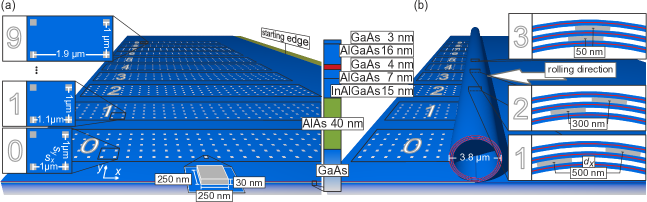
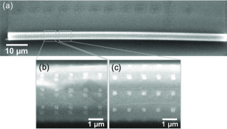
The microtubes are fabricated by rolling-up prestrained molecular-beam epitaxially grown semiconductor layers 29, 30. Figure 1 (a) illustrates the sample layout before the rolling-up process; the detailed semiconductor structure is depicted as an inset and consists of a GaAs buffer layer, a AlAs sacrificial layer, a InAlGaAs strained layer, a QW heterostructure ( AlGaAs, GaAs, AlGaAs), and a GaAs capping layer. Ultraviolet (UV) lithography is applied to create necessary structures for the rolling-up process, i.e., starting edges and shallow mesas (see, e.g., Ref. 31 for details) and to construct orientation markers for a following electron-beam (EB) lithography step, which allows to precisely define a resist mask consisting of cuboid arrays and its position with respect to the microtube’s orientation. After the lithography steps, the resist mask is transferred to Ag cuboids by depositing a -nm-thick Ag functional layer via thermal evaporation and a subsequent lift-off process. We choose cuboids of size as building blocks for the stacked nanoantennas. Their center-to-center separation in rolling direction is varied from in steps for the cuboid arrays labeled with to , see Fig. 1 (a). The cuboid separation perpendicular to the rolling direction is fixed to within each array. The rolling-up process is initiated by selective wet etching of the AlAs sacrificial layer in hydrofluoric acid. Thus, the overlying layers are released from the substrate and the strain relaxation in the InAlGaAs layer induces the self-rolling of the layers to a microtube with a typical diameter of and an adjustable rotation number. Figure 1 (b) sketches the final sample layout including a microtube with stacked Ag cuboids. The rotation number and the gap between Ag arrays and the starting edge are chosen such that two identical Ag cuboids are sandwiched between three semiconductor slabs, as depicted in the insets of Fig. 1 (b). The distances of the cuboids inside the microtube are determined by their initial lateral separation . Consequently, each of the arrays corresponds to a certain distance . For example, the cuboids of array exhibit a distance inside the microtube, the cuboids of array have a distance . The distance strongly determines the plasmonic interaction of the Ag cuboids, their coupling, and thus their properties as a compound nanoantenna. Figure 2 (a) shows a scanning-electron micrograph of the microtube investigated in this study with in length and in diameter. The cuboid arrays are visible both in their rolled-up and flat geometry. Furthermore, also lithographically defined numbers to labeling the arrays are faintly visible in the flat surface region. The magnified micrographs in Fig. 2 (b) and Fig. 2 (c) display the rolled-up Ag cuboids in array and , respectively. Here, the cuboids appear pairwise with a different contrast owing to the fact that they are sandwiched between different layers. Such a visibility of the cuboids implies a compactly rolled microtube. This allows to directly derive the cuboid distances from the geometric parameters lateral separation , distance between starting edge and arrays, individual layer thicknesses, and microtube diameter.
We investigate the coupling of the GaAs QWs to the Ag cuboid nanoantennas by means of spatially and temporally resolved PL spectroscopy. The experiments are carried out in a home-build laser scanning confocal microscope equipped with a closed-cycle cryostat operating at and with a typical spatial resolution of about . The QWs are pumped with circular polarized laser light at a wavelength of generated by an optical parametric oscillator that is driven by a pulsed Ti:sapphire laser at a wavelength of . The light is focused onto the sample with a microscope objective (100x, NA = 0.8). The same objective is used to collect the emitted light which is then coupled to a streak camera system.
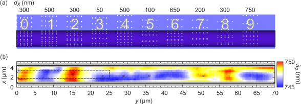
Figure 3 (a) illustrates a to-scale sketch of the sample from the top view with the microtube’s contour outlined by a black frame. The same label numbers for the Ag cuboid arrays as in Fig. 1 are used; on the top the corresponding distances of the cuboids inside the microtube are shown. The distances are directly derived from the geometric parameters and are verified with SEM images with an uncertainty of about . We raster scanned the sample in an area of with step sizes of and acquired a streak camera image at each pixel. We first evaluated the QW emission by fitting the time-integrated PL spectra with a Gaussian function. The fitted spectral position of the maximum PL intensity is plotted in the – wavelength range as a spatially-resolved false-color map in Fig. 3 (b). Fitted spectral positions outside this range are depicted as gray pixels. We also restricted the evaluation spatially to the area corresponding to the top-most section of the microtube; that way omitted pixels are plotted in gray as well. Both the plot frame of Fig. 3 (b) and the sketch in Fig. 3 (a) are matched to the same dimensions which allows to assign the arrays to the respective areas in Fig. 3 (b). The spatially resolved map of the wavelength position of the QW PL intensity maximum displayed in Fig. 3 (b) reveals red-shifted PL emission of the QWs in sections corresponding to the arrays , , , and . For these arrays the distances of the cuboids are (arrays , , and ) and (array ). The QWs in arrays with smaller distances (array with , array with ) and QWs in arrays with greater distances (array and array with , array with ) show no red-shifted PL emission. From the spatially and spectrally resolved measurements we therefore assume that the QW emission couples to the Ag cuboid nanoantenna for cuboid distances of and .
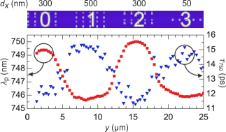
We further analyzed the time-resolved measurements by evaluating the spectrally resolved PL decay curves for the – wavelength range. The decay curves are fitted to a monoexponential function and the resulting lifetimes are denoted as . We concentrate on the scan area framed in the dashed box in Fig. 3 (b) which includes the arrays to and thus cuboid distances of , , and . The data points for and are averaged in -direction and are plotted as profiles in -direction in Fig. 4. The spectral position of the maximum PL intensity clearly shifts to and in array and , respectively. The spectral redshift is accompanied by a decrease in lifetime to and , respectively. The subtle differences in and between array 0 and 2, which have nominally the same geometries, are primarily caused by small irregularities of the cuboids themselves. According to the time-resolved measurements, the nanoantenna with selectively enhances the transition corresponding to a wavelength range from to . The enhancement of that spectral part induces an rearrangement of the quantum well spectra, i.e., the transitions corresponding to that wavelength range are highly preferred which leads to the observed redshift of the overall PL emission.
We carried out finite-element simulations with comsol multiphysics to calculate the field enhancement factor in the plane of the QWs and the overall distribution of the absolute electric field . The simulations allow to identify both the spatial and spectral overlap of emitter and plasmonic antenna and are performed for the Ag geometries corresponding to the experimentally realized distances, i.e., (array ), (array ), (array ), (array , and ), and (array and ). For simplicity we neglect the curvature of the system and assume a geometry which consists of two Ag cuboids each with size that are sandwiched between three -nm thick GaAs slabs as depicted in the sketch at the bottom of Fig. 5 (b). The semiconductor heterostructure is approximated as a homogenous GaAs layer and the values for the complex permittivities of GaAs and Ag are taken from Ref.32 and Ref. 33, respectively. The system is excited by a plane wave which is polarized in direction parallel to the cuboids’ displacement and impinging from top onto the structure.
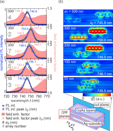
For calculating the field enhancement factors the integrated absolute electric field in the planes of the QW is normalized with respect to the integrated electric field in corresponding planes of the layered system but without Ag cuboids. The field enhancement spectra are plotted as red filled curves in Fig. 5 (a) and peaks in the spectra indicate resonant wavelengths with increased field intensities corresponding to localized surface plasmon modes. For the simulated spectra exhibit two peaks at and . For a distance of three peaks at , , and are observable. For a broad peak appears at which gets narrower and slightly red-shifted to for . Here, in addition, shoulder peaks at and are visible, respectively. For the main spectral peak shifts to the blue to . To compare with the experimental data, normalized QW emission spectra (black circles) and corresponding Gaussian fit curves (blue solid lines) taken from representative pixels marked in Fig. 3 (b) are also shown in Fig. 5 (a). It becomes obvious that there is a matching between the calculated field enhancement and the measured PL peaks only for and . In these cases, the measured PL spectra are red-shifted compared to the other spectra. This observation strongly suggests that the redshift is due to a coupling of the QW emission to the localized surface plasmon modes of the nanoantenna. For the other nanoantenna geometries, the plasmonic resonances are detuned and the QW emission spectrum remains unaltered. We further analyzed the distribution of the absolute electric field inside the Ag cuboid nanoantenna to characterize the involved plasmon modes. For this purpose we evaluate the distribution at an excitation wavelength which corresponds to the respective measured PL emission peak wavelength . Figure 5 (b) shows the cross-sectional plane of the distribution of the absolute electric field taken from the cut plane as depicted in the bottom. The different field distributions of both cuboids in each of the panel of Fig. 5 (b) are caused by retardation effects, i.e., the plane wave impinges the cuboid system from above and thus excites the upper cuboid first. For , a symmetrical high-order plasmonic mode emerges in both cuboids. Remarkably, the field intensities are distributed around each cuboid and are not condensed in a high intensity hot spot in-between. This mode distribution is also apparent in the upper cuboid for , however the field distribution of the other cuboid is altered and disturbed. For distances of , and , no symmetrically distributed plasmonic mode is visible. The resonant coupling of the QW emission to the nanoantenna with cuboid distance of is therefore associated with an excitation of a high-order plasmonic mode emerging in both cuboids.
We want to emphasize that the presented hybrid emitter/nanoantenna design is not limited to GaAs QWs and Ag cuboids. The rolling-up fabrication allows to incorporate other quantum emitters into the strained bilayer system, like self-assembled quantum dots 31, 34, 35. Furthermore, it is not limited to the InAlGaAs material system; other systems with larger band gaps like AlInP led to rolled-up structures 36 that allow for plasmonic coupling to emitters over essentially the whole visible spectral range. Besides incorporating quantum emitters directly into the strained layer system, it is also possible to utilize the strained bilayer just as a host onto which other emitters and the plasmonic nanostructures are successively deposited before the rolling process. These emitters might be thin films of colloidal nanocrystals or organic light-emitting molecules 37. Very promising, these thin films can also be lithographically structured into stripes 37 or squares before rolling. The separate preparation of emitter and metal nanostructures onto the strained bilayer enables remarkable emitter/nanoantenna designs. For example, rolling-up these emitters together with predefined Ag cuboids as used in the current work can lead to a close stacking of emitters in-between metal structures that can only hardly be realized in conventional subsequent lateral lithographic patterning alone. As for the metal part, the EB lithography approach facilitates also other antenna designs like particle dimers or bow ties. Smaller metal particles with fundamental dipole resonances in the visible spectrum allow to further modify the LSP resonance and to enhance the on-resonance near-field intensity. Besides that, the tubular geometry allows to exploit plasmon-photon whispering gallery modes 38, 28 for an even more complex tailoring of the light-matter interaction. The fabrication ansatz therefore represents an important step for the realization of quantum light sources with tailor-made optical properties.
In conclusion we report on a novel fabrication approach for a tunable plasmonic nanoantenna. We integrated Ag cuboids into a rolled-up semiconductor microtube such that two of these cuboids are stacked at a certain distance with the QW in between. The lateral distance of the cuboids is deliberately changed to tune the antenna’s resonance. By means of spatially, spectrally and temporally resolved PL measurements we show a coupling of the quantum-well emission to the nanoantenna for a cuboid distance of . We observe a redshift which is accompanied by a lifetime reduction of the the quantum-well emission. Finite-element simulations reveal that an excitation of high-order plasmonic modes inside the cuboids accounts for the resonant coupling.
We acknowledge financial support from Deutsche Forschungsgemeinschaft grant No. ME 3600/1-1. T. Kipp also acknowledges funding from the European Union’s Horizon 2020 research and innovation programme under the Marie Skłodowska-Curie grant agreement No. 656598.
References
- Ozbay 2006 Ozbay, E. Plasmonics: Merging photonics and electronics at nanoscale dimensions. Science 2006, 311, 189–193
- Lal et al. 2007 Lal, S.; Link, S.; Halas, N. J. Nano-optics from sensing to waveguiding. Nat. Photonics 2007, 1, 641–648
- Schuller et al. 2010 Schuller, J. A.; Barnard, E. S.; Cai, W. S.; Jun, Y. C.; White, J. S.; Brongersma, M. L. Plasmonics for extreme light concentration and manipulation. Nat. Mater. 2010, 9, 193–204
- Song et al. 2005 Song, J. H.; Atay, T.; Shi, S. F.; Urabe, H.; Nurmikko, A. V. Large enhancement of fluorescence efficiency from CdSe/ZnS quantum dots induced by resonant coupling to spatially controlled surface plasmons. Nano Lett. 2005, 5, 1557–1561
- Pompa et al. 2006 Pompa, P. P.; Martiradonna, L.; Della Torre, A.; Della Sala, F.; Manna, L.; De Vittorio, M.; Calabi, F.; Cingolani, R.; Rinaldi, R. Metal-enhanced fluorescence of colloidal nanocrystals with nanoscale control. Nat. Nanotechnol. 2006, 1, 126–130
- Kuhn et al. 2006 Kuhn, S.; Hakanson, U.; Rogobete, L.; Sandoghdar, V. Enhancement of single-molecule fluorescence using a gold nanoparticle as an optical nanoantenna. Phys. Rev. Lett. 2006, 97, 017402
- Taminiau et al. 2008 Taminiau, T. H.; Stefani, F. D.; Segerink, F. B.; Van Hulst, N. F. Optical antennas direct single-molecule emission. Nat. Photonics 2008, 2, 234–237
- Tanaka et al. 2010 Tanaka, K.; Plum, E.; Ou, J. Y.; Uchino, T.; Zheludev, N. I. Multifold Enhancement of Quantum Dot Luminescence in Plasmonic Metamaterials. Phys. Rev. Lett. 2010, 105, 227403
- Kinkhabwala et al. 2009 Kinkhabwala, A.; Yu, Z. F.; Fan, S. H.; Avlasevich, Y.; Mullen, K.; Moerner, W. E. Large single-molecule fluorescence enhancements produced by a bowtie nanoantenna. Nat. Photonics 2009, 3, 654–657
- Acuna et al. 2012 Acuna, G. P.; Moller, F. M.; Holzmeister, P.; Beater, S.; Lalkens, B.; Tinnefeld, P. Fluorescence Enhancement at Docking Sites of DNA-Directed Self-Assembled Nanoantennas. Science 2012, 338, 506–510
- Akselrod et al. 2016 Akselrod, G. M.; Weidman, M. C.; Li, Y.; Argyropoulos, C.; Tisdale, W. A.; Mikkelsen, M. H. Efficient Nanosecond Photoluminescence from Infrared PbS Quantum Dots Coupled to Plasmonic Nanoantennas. Acs Photonics 2016, 3, 1741–1746
- Anger et al. 2006 Anger, P.; Bharadwaj, P.; Novotny, L. Enhancement and quenching of single-molecule fluorescence. Phys. Rev. Lett. 2006, 96, 113002
- Muskens et al. 2007 Muskens, O. L.; Giannini, V.; Sanchez-Gil, J. A.; Rivas, J. G. Strong enhancement of the radiative decay rate of emitters by single plasmonic nanoantennas. Nano Lett. 2007, 7, 2871–2875
- Ma et al. 2010 Ma, X. D.; Tan, H.; Kipp, T.; Mews, A. Fluorescence Enhancement, Blinking Suppression, and Gray States of Individual Semiconductor Nanocrystals Close to Gold Nanoparticles. Nano Lett. 2010, 10, 4166–4174
- Le Ru et al. 2007 Le Ru, E. C.; Etchegoin, P. G.; Grand, J.; Felidj, N.; Aubard, J.; Levi, G. Mechanisms of spectral profile modification in surface-enhanced fluorescence. J. Phys. Chem. C 2007, 111, 16076–16079
- Ringler et al. 2008 Ringler, M.; Schwemer, A.; Wunderlich, M.; Nichtl, A.; Kurzinger, K.; Klar, T. A.; Feldmann, J. Shaping emission spectra of fluorescent molecules with single plasmonic nanoresonators. Phys. Rev. Lett. 2008, 100, 203002
- Zhao et al. 2011 Zhao, L.; Ming, T.; Chen, H. J.; Liang, Y.; Wang, J. F. Plasmon-induced modulation of the emission spectra of the fluorescent molecules near gold nanorods. Nanoscale 2011, 3, 3849–3859
- Fromm et al. 2004 Fromm, D. P.; Sundaramurthy, A.; Schuck, P. J.; Kino, G.; Moerner, W. E. Gap-dependent optical coupling of single "Bowtie" nanoantennas resonant in the visible. Nano Lett. 2004, 4, 957–961
- Curto et al. 2010 Curto, A. G.; Volpe, G.; Taminiau, T. H.; Kreuzer, M. P.; Quidant, R.; van Hulst, N. F. Unidirectional Emission of a Quantum Dot Coupled to a Nanoantenna. Science 2010, 329, 930–933
- Dregely et al. 2011 Dregely, D.; Taubert, R.; Dorfmuller, J.; Vogelgesang, R.; Kern, K.; Giessen, H. 3D optical Yagi-Uda nanoantenna array. Nat. Commun. 2011, 2, 267
- Ameling and Giessen 2010 Ameling, R.; Giessen, H. Cavity Plasmonics: Large Normal Mode Splitting of Electric and Magnetic Particle Plasmons Induced by a Photonic Microcavity. Nano Lett. 2010, 10, 4394–4398
- Bakker et al. 2008 Bakker, R. M.; Yuan, H. K.; Liu, Z. T.; Drachev, V. P.; Kildishev, A. V.; Shalaev, V. M.; Pedersen, R. H.; Gresillon, S.; Boltasseva, A. Enhanced localized fluorescence in plasmonic nanoantennae. Appl. Phys. Lett. 2008, 92, 043101
- Schwaiger et al. 2009 Schwaiger, S.; Broll, M.; Krohn, A.; Stemmann, A.; Heyn, C.; Stark, Y.; Stickler, D.; Heitmann, D.; Mendach, S. Rolled-Up Three-Dimensional Metamaterials with a Tunable Plasma Frequency in the Visible Regime. Phys. Rev. Lett. 2009, 102, 163903
- Rottler et al. 2012 Rottler, A.; Harland, M.; Broll, M.; Schwaiger, S.; Stickler, D.; Stemmann, A.; Heyn, C.; Heitmann, D.; Mendach, S. Rolled-up nanotechnology for the fabrication of three-dimensional fishnet-type GaAs-metal metamaterials with negative refractive index at near-infrared frequencies. Appl. Phys. Lett. 2012, 100, 151104
- Zhang et al. 2015 Zhang, Y.; Han, D.; Du, D. Y.; Huang, G. S.; Qiu, T.; Mei, Y. F. Rolled-Up Ag-SiOx Hyperbolic Metamaterials for Surface-Enhanced Raman Scattering. Plasmonics 2015, 10, 949–954
- Schulz et al. 2016 Schulz, K. M.; Vu, H.; Schwaiger, S.; Rottler, A.; Korn, T.; Sonnenberg, D.; Kipp, T.; Mendach, S. Controlling the Spontaneous Emission Rate of Quantum Wells in Rolled-Up Hyperbolic Metamaterials. Phys. Rev. Lett. 2016, 117, 085503
- Zhang et al. 2015 Zhang, J.; Li, J. X.; Tang, S. W.; Fang, Y. F.; Wang, J.; Huang, G. S.; Liu, R.; Zheng, L. R.; Cui, X. G.; Mei, Y. F. Whispering-gallery nanocavity plasmon-enhanced Raman spectroscopy. Sci. Rep. 2015, 5, 15012
- Yin et al. 2016 Yin, Y.; Li, S. L.; Bottner, S.; Yuan, F. F.; Giudicatti, S.; Naz, E. S. G.; Ma, L. B.; Schmidt, O. G. Localized Surface Plasmons Selectively Coupled to Resonant Light in Tubular Microcavities. Phys. Rev. Lett. 2016, 116, 253904
- Prinz et al. 2000 Prinz, V. Y.; Seleznev, V. A.; Gutakovsky, A. K.; Chehovskiy, A. V.; Preobrazhenskii, V. V.; Putyato, M. A.; Gavrilova, T. A. Free-standing and overgrown InGaAs/GaAs nanotubes, nanohelices and their arrays. Physica E 2000, 6, 828–831
- Schmidt and Eberl 2001 Schmidt, O. G.; Eberl, K. Nanotechnology - Thin solid films roll up into nanotubes. Nature 2001, 410, 168–168
- Mendach et al. 2006 Mendach, S.; Songmuang, R.; Kiravittaya, S.; Rastelli, A.; Benyoucef, M.; Schmidt, O. G. Light emission and wave guiding of quantum dots in a tube. Appl. Phys. Lett. 2006, 88, 111120
- Aspnes and Studna 1983 Aspnes, D. E.; Studna, A. A. Dielectric Functions and Optical-parameters of Si, Ge, Gap, Gaas, Gasb, Inp, Inas, and Insb From 1.5 To 6.0 Ev. Phys. Rev. B 1983, 27, 985–1009
- Johnson and Christy 1972 Johnson, P. B.; Christy, R. W. Optical Constants of Noble Metals. Phys. Rev. B 1972, 6, 4370–4379
- Kipp et al. 2006 Kipp, T.; Welsch, H.; Strelow, C.; Heyn, C.; Heitmann, D. Optical modes in semiconductor microtube ring resonators. Phys. Rev. Lett. 2006, 96, 077403
- Li et al. 2009 Li, F.; Vicknesh, S.; Mi, Z. Optical modes in InGaAs/GaAs quantum dot microtube ring resonators at room temperature. Electron. Lett. 2009, 45, 645–U20
- Strelow et al. 2012 Strelow, C.; Kietzmann, S.; Schramm, A.; Seher, R.; Penttinen, J. P.; Hakkarainen, T. V.; Mews, A.; Kipp, T. AlInP-based rolled-up microtube resonators with colloidal nanocrystals operating in the visible spectral range. Appl. Phys. Lett. 2012, 101, 113114
- Kietzmann et al. 2015 Kietzmann, S.; Strelow, C.; Tavares, L.; Penttinen, J. P.; Hakkarainen, T. V.; Schramm, A.; Osadnik, A.; Lutzen, A.; Kjelstrup-Hansen, J.; Mews, A.; Kipp, T. Organic Molecular Films as Light-Emitting and Light-Confining Material in Rolled-Up AlInP Semiconductor Microtube Resonators. Acs Photonics 2015, 2, 1532–1538
- Rottler et al. 2013 Rottler, A.; Harland, M.; Broll, M.; Klingbeil, M.; Ehlermann, J.; Mendach, S. High-Q Hybrid Plasmon-Photon Modes in a Bottle Resonator Realized with a Silver-Coated Glass Fiber with a Varying Diameter. Phys. Rev. Lett. 2013, 111, 253901