Coherent spin-transfer precession switching in orthogonal spin-torque devices
Abstract
We present experimental results and macrospin simulations of the switching characteristics of orthogonal spin-transfer devices incorporating an out-of-plane magnetized polarizing layer and an in-plane magnetized spin valve device at cryogenic temperatures. At we demonstrate: high speed deterministic switching at short pulse lengths — down to — with sufficient measurement statistics to establish a switching error rate of ; coherent precessional switching at longer times; and observe ensemble decoherence effects at even longer times. Finite temperature macrospin models model the precessional switching well but fail to fully reproduce all the decoherence and switching error behaviour.
Spin-transfer devices that operate at low temperature are of interest for applications that require a cryogenic memory, such as Josephson junction based logic circuits Holmes, Ripple, and Manheimer (2013). A requirement for this application is high speed operation with relatively low energy dissipation. Conventional spin transfer torque (STT) devices, such as those being developed as commercial room temperature memories, may not be suitable for low temperature operation if the switching is thermally activated and may not take advantage of the lower power possible at low temperatures. A conventional STT device consists of two thin magnetic layers separated by a non-magnetic layer, with the memory states being the layer magnetizations aligned either parallel or antiparallel. However, the initial spin-transfer torque in these states is vanishingly small, and a spin polarized current amplifies thermal fluctuations of the magnetization, leading to nanosecond incubation delays for switching and stochastic switching characteristics Brataas, Kent, and Ohno (2012); Devolder et al. (2008); Liu et al. (2014). At low temperature this mechanism of STT writing should be even slower and less energy efficient.

An orthogonal spin-transfer (OST) device overcomes this limitation by having a spin-polarizing layer aligned perpendicular to the free layer that provides a large spin-torque the moment a current is applied Kent, Özyilmaz, and Del Barco (2004). This perpendicular polarizer induces precessional magnetization dynamics, as it forces the free layer magnetization out of the film plane leading to coherent precessional motion of the magnetization about the film normal, the magnet’s hard magnetic axis Houssameddine et al. (2007). Experiments at room temperature have demonstrated both fast () switching as well as the excitation of precessional magnetization dynamics Lee et al. (2009); Papusoi et al. (2009); Beaujour et al. (2009); Liu et al. (2010); Rowlands et al. (2011); Liu et al. (2012) while recent experiments at low temperature have demonstrated even faster () and deterministic switching in OST-devices Park, Ralph, and Buhrman (2013); Ye et al. (2014). These experiments were conducted over a relatively limited range of applied currents and pulse durations, and thus could not probe the coherent magnetization dynamics expected at low temperature.
Here we study switching in OST spin-value based devices at with an improved experimental setup focused on minimizing thermal noise at the device increasing the data taking rate. This enables us to measure a range of pulse amplitudes and durations to observe phase diagrams of coherent magnetization dynamics. We also demonstrate deterministic high speed switching for pulse lengths down to and establish bounds on the switching error rates not limited by measurement statistics. We model our results with a finite-temperature stochastic Landau-Lifshitz-Gilbert-Slonczewski (LLGS) model Slonczewski (1996) and find that even at cryogenic temperatures, thermal noise or micro-magnetic effects can lead to an incoherent decay in the switching probabilities.

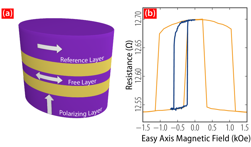
The OST devices under study consist of a CoFeB(3) magnetic free layer (FL), a CoFeB(12) reference layer (RL), and a [Co(0.3)/Pd(0.7)]2/[Co(0.15)/Ni(0.6)]3 perpendicularly magnetized spin-polarizing layer (PL) arranged into a full stack of PL/Cu(10)/FL/Cu(10)/RL as shown in Figure 1(a). All dimensions are given in nm. Nanopillars of various shapes and aspect ratios were fabricated using e-beam lithography and ion-milling. Here we present results for devices with a elliptical cross-section, whose FLs have shape anisotropy that defines a magnetic easy axis in the film plane along the long axis of ellipse. Shape anisotropy also sets the magnetization direction of the thicker RL. The major and minor hysteresis loops of one such device are shown in Figure 1(b). A clear offset of the minor loop is observed because of the uncompensated dipole field from the RL.
Sample chips are mounted and wirebonded in a custom package designed to support microwave signals. The package is mounted on the cold-head of Gifford-McMahon cryocooler (Sumitomo RDK-101D) with a base temperature of when loaded with coaxial lines. Switching pulses are provided by either a pulse generator (Picosecond Pulse Labs 10,070A) or an AWG (Keysight M8190A) that are combined and then capacitively coupled to the device via a bias-T (Picosecond Pulse Labs 5575A) mounted at the cold head. The high speed line has cryogenic attenuators at both the and stages to thermalize the center conductor and attenuate thermal noise from higher temperature stages. To provide additional pulse amplitude resolution for the pulse generator (above the resolution of the internal step attenuator) we use a voltage controlled variable attenuator (RFMD RFSA2113 evaluation board). The DC coupled port of the bias-T is used to apply current bias and make resistance measurements using a lock-in amplifier (SRS 865) operated at a baseband. The measurement line is low-pass filtered with a custom ECCOSORB low-pass filter Santavicca and Prober (2008) at the stage again to suppress thermal noise from room temperature. The external magnetic field is applied by a room-temperature electromagnet. A block diagram of the setup is shown in Figure 2(a).
Switching studies are performed with a bias field set in the center of the minor hysteresis loop of Figure 1(b). Since precessional switching can be induced irrespective of polarity, we use the AWG to supply a fixed-polarity “reset” pulse whose width and amplitude produce high probability switching regardless of whether the system starts in the antiparallel (AP) or parallel (P) configuration of the FL and RL. Reset pulses are applied every second shot followed by the switching pulse applied using the pulse generator. This procedure allows us measure both APP and PAP transitions in the same data run. To maximize the data acquisition rate, the experiment is sequenced by the AWG and is continuously streamed at rate of until the desired switching statistics are achieved. The voltages from the lock-in were clustered into two or three clusters using a kmeans algorithm Macqueen (1967) (see Figure 2(b)). With a sufficient settling time for the lock-in the distributions are approximately Gaussian — insomuch as they are visually indistinguishable from a normal distribution despite failing the Anderson-Darling test for normality — and well separated. Taking the Gaussian assumption the probability of misclassification of the state is infinitesimally small at and thus the reported switching error rates are intrinsic to the device. The third cluster was used for when we occasionally saw an unresponsive intermediate resistance (IR) state Ye et al. (2015), most commonly after the application of high amplitude switching pulses. Typically, the device would remain stuck in this IR state for a short period of time but occasionally would need to be forced out with a magnetic field sweep. We hypothesize that this state arises from a non-uniform magnetization state in the FL and/or RL that decreases the switching efficiency of STT induced reversal.

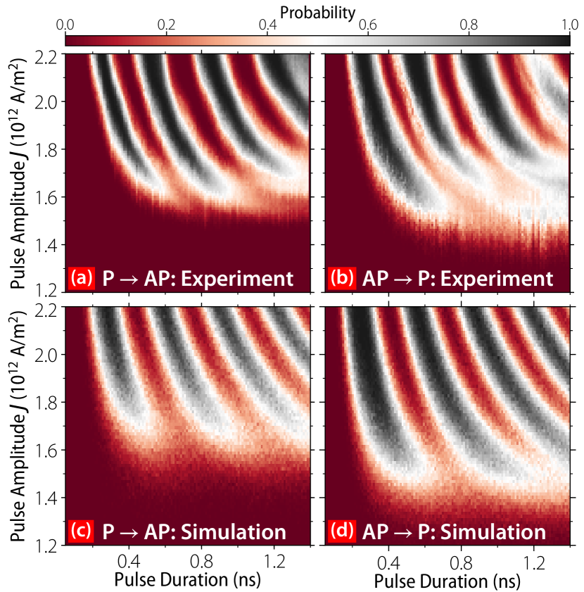
We apply this measurement procedure over a range of pulse amplitudes and durations in order to build up a phase diagram for precessional switching. These results are shown in Figs. 3(a-b), where each pixel represents the switching probability calculated as the mean of the beta distribution for the switching attempts in each direction (we take 4096 shots for each pair of pulse amplitude and duration settings and with the reset pulse every second shot the initial state distribution is ). In both APP and PAP polarities, the sample undergoes three full probability oscillations with a period of approximately . For longer pulses the switching probability does not recover to 100%, and for longer pulses yet (not shown) the sample can occasionally become stuck in the intermediate resistance state mentioned above.
To better understand these results we perform finite temperature simulations of macrospin model of Eq. 1 using our parallel, GPU enabled, macrospin_gpu package Rowlands (2017). The simulated dynamics are described by the LLGS equation:
| (1) |
where is the FL magnetization unit vector, the deterministic LLG torque, the thermal torque, and the STT. The LLG torque, , is given in terms of the effective field for FL volume and damping constant . Time in Eq. 1 has been normalized by the precession frequency so that , where is the gyromagnetic ratio. The thermal torque is induced by a Gaussian distributed random field Brown (1963). Although this is a standard assumption we note its applicability to the present regime of cryogenic temperatures and sub-nanosecond switching times is not established. The combined spin-torque contributions from both the out-of-plane PL and in-plane RL can be described in terms of effective spin-polarization vector :
| (2) | ||||
| (3) |
Here and are the spin-torque polarization and asymmetry parameters Slonczewski (2002), respectively, encodes the angular dependence of the spin torque for an angle between the spin torque polarization and FL, and is the normalized applied current.
As in the experiments we simulate the entire amplitude-duration phase diagram, shown in Figs. 3(c-d), where each pixel gives the switching probability for an ensemble of 512 macrospins subject to different realizations of the thermal field. We take , , , . The shape anisotropy is treated as the combination of two uniaxial contributions: an out-of-plane hard-axis demagnetizing field and an in-plane easy-axis field Oe. The dipolar field from the reference layer is assumed to be cancelled by the external field and is omitted in our simulations. The ensemble is allowed to thermalize in the AP or P state before a current pulse (rise/fall time of ) is applied. The simulations reproduce the shape and periodicity of the probability oscillations. The disparity in critical current densities for different switching polarities, as well as the slightly increased APP switching speed is caused by the influence of STT from the in-plane RL Ye et al. (2015). For negative pulses (not shown), we find reduced switching probabilities that are indicative of a non-zero Park, Ralph, and Buhrman (2013).

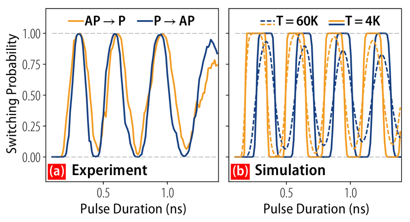
The simulations of Figs. 3(c-d) are performed at in order to produce a broadening of the switching bands consistent with the experimental data. Comparing constant pulse-amplitude slices of the simulated and experimental phase diagrams, as shown in Figs. 4(a,b), reveals some distinct differences. At the experimental probability oscillations exhibit a sinusoidal behavior before a precipitous decline in probability upon the final oscillation. Meanwhile, the simulated oscillations exhibit wide high-probability bands with a minimal amount of rounding. At the simulations show a gradual decoherence of the ensemble resulting from dephasing along the out-of-plane switching trajectories. Pinna, Stein, and Kent (2014) This behavior is not observed in the experimental data, and we hypothesize that a micromagnetic instability (perhaps in the form of domain nucleation) is responsible for the abrupt departure from full-probability oscillations. The more complicated sub-structure of the experimental switching phase diagrams near threshold may also result from micromagnetic considerations.
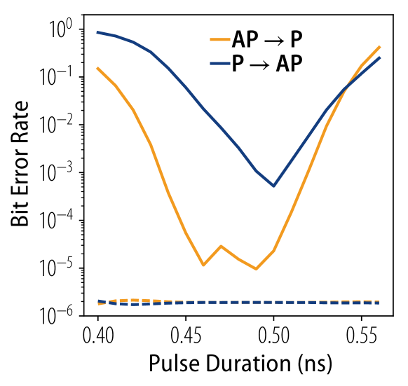
The experimental APP and PAP transition probabilities in Fig. 4(a) are synchronized such that they are maximized for the same pulse durations, in contrast to the behavior of the macrospin simulations in Fig. 4(b). This has important implications for memory write circuitry, which would suffer a substantial increase in complexity were it required to generate different pulses of different amplitudes. We explore the bit error rates (BER) near the maximum of the second probability oscillation, as shown in Figure 5. We find that APP switching reaches error rates over a fairly broad window of pulse widths. For PAP switching, there is a comparatively narrow window where switching reaches a BER of .

In conclusion, we have measured high-resolution switching phase diagrams for orthogonal spin-torque devices that reveal precessional reversal. Finite temperature macrospin simulations reproduce many of the qualitative features of this reversal, and allow us to identify the clear influence of STT from both the PL and RL. Simulations cannot reproduce the sinusoidal probability oscillations without introducing strong dephasing, nor can they account for the coincidence between APP and PAP switching probability maxima. Further work, particularly in the area of micromagnetic simulations, is required to understand the origin of these features.
We thank Robert Buhrman for many productive discussions. Measurements are performed using the Auspex package Rowlands, Ryan, and Johnson (2017). The macrospin simulations were performed using the macrospin_gpu package Rowlands (2017). Data analysis was performed in Julia Bezanson et al. (2014) with k-means clustering from the Clustering.jl packageLin and White (2016). The figures were made using matplotlib Hunter (2007). The research is based on work supported by the Office of the Director of National Intelligence (ODNI), Intelligence Advanced Research Projects Activity (IARPA), via contract W911NF-14-C0089. The views and conclusions contained herein are those of the authors and should not be interpreted as necessarily representing the official policies or endorsements, either expressed or implied, of the ODNI, IARPA, or the U.S. Government. The U.S. Government is authorized to reproduce and distribute reprints for Governmental purposes notwithstanding any copyright annotation thereon. This document does not contain technology or technical data controlled under either the U.S. International Traffic in Arms Regulations or the U.S. Export Administration Regulations.
References
- Holmes, Ripple, and Manheimer (2013) D. S. Holmes, A. L. Ripple, and M. A. Manheimer, “Energy-Efficient Superconducting Computing—Power Budgets and Requirements,” IEEE Transactions on Applied Superconductivity 23, 1701610–1701610 (2013).
- Brataas, Kent, and Ohno (2012) A. Brataas, A. D. Kent, and H. Ohno, “Current-induced torques in magnetic materials,” (2012).
- Devolder et al. (2008) T. Devolder, J. Hayakawa, K. Ito, H. Takahashi, S. Ikeda, P. Crozat, N. Zerounian, J. V. Kim, C. Chappert, and H. Ohno, “Single-shot time-resolved measurements of nanosecond-scale spin-transfer induced switching: Stochastic versus deterministic aspects,” Physical Review Letters 100 (2008), 10.1103/PhysRevLett.100.057206.
- Liu et al. (2014) H. Liu, D. Bedau, J. Z. Sun, S. Mangin, E. E. Fullerton, J. A. Katine, and A. D. Kent, “Dynamics of spin torque switching in all-perpendicular spin valve nanopillars,” Journal of Magnetism and Magnetic Materials 358-359, 233–258 (2014).
- Kent, Özyilmaz, and Del Barco (2004) A. D. Kent, B. Özyilmaz, and E. Del Barco, “Spin-transfer-induced precessional magnetization reversal,” Applied Physics Letters 84, 3897–3899 (2004).
- Houssameddine et al. (2007) D. Houssameddine, U. Ebels, B. Delaët, B. Rodmacq, I. Firastrau, F. Ponthenier, M. Brunet, C. Thirion, J.-P. Michel, L. Prejbeanu-Buda, M.-C. Cyrille, O. Redon, and B. Dieny, “Spin-torque oscillator using a perpendicular polarizer and a planar free layer.” Nature materials 6, 441–447 (2007).
- Lee et al. (2009) O. J. Lee, V. S. Pribiag, P. M. Braganca, P. G. Gowtham, D. C. Ralph, and R. A. Buhrman, “Ultrafast switching of a nanomagnet by a combined out-of-plane and in-plane polarized spin current pulse,” Applied Physics Letters 95, 12506 (2009), arXiv:0906.2585 .
- Papusoi et al. (2009) C. Papusoi, B. Delat, B. Rodmacq, D. Houssameddine, J. P. Michel, U. Ebels, R. C. Sousa, L. Buda-Prejbeanu, and B. Dieny, “100 ps precessional spin-transfer switching of a planar magnetic random access memory cell with perpendicular spin polarizer,” Applied Physics Letters 95 (2009), 10.1063/1.3206919.
- Beaujour et al. (2009) J.-M. L. Beaujour, D. B. Bedau, H. Liu, M. R. Rogosky, and A. D. Kent, “Spin-Transfer in Nanopillars with a Perpendicularly Magnetized Spin Polarizer,” Proceedings of the SPIE - The International Society for Optical Engineering 7398, 73980D–73980D–11 (2009).
- Liu et al. (2010) H. Liu, D. Bedau, D. Backes, J. A. Katine, J. Langer, and A. D. Kent, “Ultrafast switching in magnetic tunnel junction based orthogonal spin transfer devices,” Applied Physics Letters 97, 242510 (2010).
- Rowlands et al. (2011) G. E. Rowlands, T. Rahman, J. A. Katine, J. Langer, A. Lyle, H. Zhao, J. G. Alzate, A. A. Kovalev, Y. Tserkovnyak, Z. M. Zeng, H. W. Jiang, K. Galatsis, Y. M. Huai, P. K. Amiri, K. L. Wang, I. N. Krivorotov, and J. Wang, “Deep subnanosecond spin torque switching in magnetic tunnel junctions with combined in-plane and perpendicular polarizers,” Appl. Phys. Lett. 98, 102509 (2011).
- Liu et al. (2012) H. Liu, D. Bedau, D. Backes, J. A. Katine, and A. D. Kent, “Precessional reversal in orthogonal spin transfer magnetic random access memory devices,” Applied Physics Letters 101, 032403 (2012).
- Park, Ralph, and Buhrman (2013) J. Park, D. C. Ralph, and R. A. Buhrman, “Fast deterministic switching in orthogonal spin torque devices via the control of the relative spin polarizations,” Applied Physics Letters 103, 252406 (2013).
- Ye et al. (2014) L. Ye, D. B. Gopman, L. Rehm, D. Backes, G. Wolf, T. Ohki, A. F. Kirichenko, I. V. Vernik, O. A. Mukhanov, and A. D. Kent, “Spin-transfer switching of orthogonal spin-valve devices at cryogenic temperatures,” J. Appl. Phys. 115, 17C725 (2014).
- Slonczewski (1996) J. Slonczewski, “Current-driven excitation of magnetic multilayers,” Journal of Magnetism and Magnetic Materials 159, L1–L7 (1996).
- Santavicca and Prober (2008) D. F. Santavicca and D. E. Prober, “Impedance-matched low-pass stripline filters,” Measurement Science and Technology 087001, 9 (2008), arXiv:0802.1343 .
- Macqueen (1967) J. Macqueen, “Some methods for classification and analysis of multivariate observations,” Proceedings of the Fifth Berkeley Symposium on Mathematical Statistics and Probability 1, 281–297 (1967).
- Ye et al. (2015) L. Ye, G. Wolf, D. Pinna, G. D. C.-o. Flynn, and A. D. Kent, “State diagram of an orthogonal spin transfer spin valve device,” J. Appl. Phys. 117, 193902 (2015).
- Rowlands (2017) G. E. Rowlands, “macrospin_gpu: v0.1.0 (January 2017),” (2017).
- Brown (1963) W. F. Brown, “Thermal Fluctuations of a Single-Domain Particle,” Physical Review 130, 1677–1686 (1963).
- Slonczewski (2002) J. C. Slonczewski, “Currents and torques in metallic magnetic multilayers,” Journal of Magnetism and Magnetic Materials 247, 324–338 (2002).
- Pinna, Stein, and Kent (2014) D. Pinna, D. L. Stein, and A. D. Kent, “Spin-torque oscillators with thermal noise: A constant energy orbit approach,” Phys. Rev. B - Condens. Matter Mater. Phys. 90, 174405 (2014), arXiv:1405.0731 .
- Rowlands, Ryan, and Johnson (2017) G. E. Rowlands, C. A. Ryan, and B. R. Johnson, “Auspex: v0.3.0 (January 2017),” (2017).
- Bezanson et al. (2014) J. Bezanson, A. Edelman, S. Karpinski, and V. B. Shah, “Julia: A Fresh Approach to Numerical Computing,” , 41 (2014), arXiv:1411.1607 .
- Lin and White (2016) D. Lin and J. M. White, “Clustering.jl,” https://github.com/JuliaStats/Clustering.jl (2016).
- Hunter (2007) J. D. Hunter, “Matplotlib: A 2D graphics environment,” Computing in Science and Engineering 9, 99–104 (2007).