Interaction of Adatoms with Two-Dimensional Metal Monochalcogenides (GaS, GaSe)
Abstract
In this paper, we report first principles calculations based on density functional theory to reveal the effects of selected adatoms (Li, Na, K, Be, Mg, Ca, B, C, N, O, Al, Si, P, Ga, Ge, As, Se and S) adsorption on GaX ( where X=S, Se) monolayers. It is found that all adatoms adsorbed on GaX monolayers can form strong chemisorption bonds except for Mg atom due to weak bonding nature of Mg atom with early 3d transition metals. Most of the adatoms of the same group elements of the periodic table are bound to GaX substrates at the same adsorption sites. All adatoms stayed above the upper layer of GaX sheets except for Be adatom on GaSe substrate and overall hexagonal geometry has been retained. The electronic structures are modified by locally through the supercell calculations. Specific adatoms, such as C, Si, Ge, N, P and As give rise to spin polarization and attain integer magnetic moments and hence can contribute half metallic character to the system. Our results can serve as a basis for future experimental and theoretical studies of adsorption on GaX.
I Introduction
Recently, monolayer structure of metal monochalcogenides have been produced with exfoliation techniques and the electronic, magnetic, mechanical and optical properties of these monolayers[1, 2, 3, 4, 5, 6] have been an active subject of theoretical and experimental studies. These are GaX, in which there are two sheets of Ga layers sandwiched between chalcogenide layers (in order of X-Ga-Ga-X, where X=S, Se, Te). Even before most research has focused on monolayer structures of GaX, bulk GaX with layered structure have been widely used in diverse fields due to many interesting electronic and optical properties. [7, 8, 9, 10, 11] These layered structures have a highly anisotropic bonding force, because layer-layer interaction has very weak van der Waals (vdW) force than the bonding force within the layer. GaX is consisted of both covalent Ga-Ga bonds and cation(Ga)-anion(X) bonds by contrast with many other layer compounds, and due to this extremely weak vdW force they can be easily cleaved along layers. There have been a number of experimental efforts to fabricate the two-dimensional (2D) GaX monolayers[12, 13, 14] since they are stable layered semiconducting materials with wide band gaps. Based upon only comprising light elements of GaX monolayers, they have attracted interest due to their potential applications in fields such as solar energy conversion[15]. For instance, multilayer GaS1-xSex (0x1) were synthesized by means of chemical vapor transport (CVT) by Jung et al. and showed that GaS-GaSe alloys have band gaps in the range of 2.0-2.5 eV which are matching the visible region of spectrum with red to green[16]. Tongay et al. have recently reported that the effects of different gas molecules on photoelectric response of few-layer defected GaSe phototransistors[17], and they proved that existing of O2 molecule can increase the performance of GaSe phototransistors compared to that in the air. However, similar study on GaS monolayer showed that photo-response of GaS nanosheet is higher in NH3 environment instead of that in the air or O2 environment[18].
In fact, GaSe triangular monolayer flakes are grown on SiO2/Si substrates, but these flakes show randomly distributed orientations, therefore, when these triangulars merge to form larger sheet, grain boundaries occur and that cause to decrease electrical properties[2]. Recently, the same group synthesized preferred orientations of 2D GaSe atomic layers on graphene by vdW epitaxy, therefore larger GaSe monolayers can grow[19]. At the same time, dielectric and electronic properties of monolayer and multilayer GaS and GaSe are investigated and obtained that electron energy low-loss spectra shifts towards larger wavelength with decrease of layer thickness[20, 21]. Furthermore, Peng systematically increased Mg doping in GaS and GaSe monolayer which causes p-type carriers in GaSe nanosheets[22]. While GaS and GaSe monolayer is a semicondutor, Ga vacancy induces ferromagnetism and half-metallicity, however S or Se hole doping rendering GaS and GaSe n-type semiconductors[23, 24, 25]. Moreover, substitutional impurity effect is studied for GaX (X=S, Se) monolayers by doping transition metal and nonmetal atoms where the results give a net magnetic moments increase from 1 to 5 [25, 26].
Although there are numerous experimental and theoretical studies on the exfoliation of GaX monolayers or the investigation of their structural, optical, and electronic properties, we have not encountered any studies about the effects of adatom adsorption on GaS or GaSe monolayer (except of gas molecule adsorption[16, 17, 18]). In contrast to MX2 or MX3 monolayers, GaS and GaSe monolayers include light elements only, so it will be important to investigate how the electronic and magnetic properties of GaS (or GaSe) monolayers change when the light elements adsorbed on them. For this reason, in this study, we systematically investigate the effects of light elements (Li, Na, K, Be, Mg, Ca, B, C, N, O, Al, Si, P, Ga, Ge, As, Se and S) on the GaS and GaSe monolayers. Our study reveals interesting results, which are important for further study and applications of GaX monolayers. These are as follows: (i) Our results indicate that all adatoms except Mg are bound to GaX monolayers with significant binding energy. (ii) Mostly the same group elements of periodic table, prefer to locate at the same adsorption sites for both on GaX substrates. The electronic structures are modified by adatom adsorption and the nonmagnetic indirect band gap semiconductors attain net magnetic moment through the adsorption C, Si, Ge, N, P and As adatoms.
II Computational Methodology
We have performed first-principles plane wave calculations based on the spin-polarized density functional theory (DFT)[27] using projector augmented wave (PAW)[28] potentials. The exchange correlation potential is approximated by a generalized gradient approximation (GGA) using the Perdew-Burke-Ernzerhof (PBE) functional [29] . The van der Waals (vdW) correction to the functional is included by using the DFT-D2 method of Grimme[30]. Adsorption of all adatoms are investigated using GaX supercells. Electronic and geometric relaxations of the structures are performed using supercells for GaS (or Se) sheets which are large enough to avoid interactions between adjacent adatoms, since, this size of cell is 4-5 times larger than dimer length of considered adatoms. The vacuum spacing between the layers are taken at least 15 Å. Based on the convergence analysis on kinetic energy cutoff and k-point sampling, a plane-wave basis set with kinetic energy cutoff is taken to be 400 eV (600 eV for oxygen adsorption) and the Brillouin zone (BZ) is sampled in the k-space within -centered. Atomic positions are optimized using the conjugate gradient method, where all the atomic coordinates are fully relaxed until the force is less than 0.001 eV/Å and the energy convergence value between two consecutive steps is chosen as eV. Gaussian type Fermi-level smearing method is used with a smearing width of 0.01 eV. The total energies and electronic density of states of bare and adatom adsorbed structures are calculated by using PBE method. Nevertheless, energy band gaps are underestimated by DFT, we corrected bare GaS and GaSe monolayer band energies by using Hybrid Heyd-Scuseria-Ernzerhof (HSE) method[31, 32, 33]. All the numerical calculations are performed using the Vienna ab-initio Simulation Package (VASP)[34, 35] code.
The magnetic ground states of adatom+substrate systems revealed by the optimization based on spin-polarized DFT are further elaborated. In order to obtain the magnetic moments, the structure is first completely relaxed by spin-polarized calculations. Charge transfer between adatom and monolayer GaS/GaSe , is calculated by using Bader analysis[36]. The difference charge density, , is calculated by subtracting the charge density of pristene GaS/GaSe sheets , and that of free adatom , from the total charge density of the optimized adatom+substrate structure . Positive values of correspond to charge donation from the adatom to substrate, negative sign for vice versa. The adsorption energies of adatoms are obtained by Eads = Eadatom - EGaX - Eadatom+GaX. Here Eadatom, EGaX, Eadatom+GaX are the ground state energies of isolated adatom, bare GaS/GaSe sheets, and the adatom adsorbed GaS/GaSe system, respectively.
III Bare GaX (X = S, Se) Monolayer
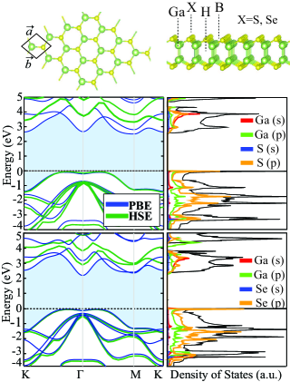
Before discussing the adatom adsorption, we first examine the structural and electronic properties of bare 2D hexagonal GaX monolayer structures for understanding and analysis of interaction between bare system with adatoms. Atomic configuration of GaX monolayer is shown in Fig. 1, where the crystal consists of 4 atoms (X-Ga-Ga-X) in unitcell and X (chalcogenide atom) stands for S or Se atoms.
The calculated values of lattice constants for GaS and GaSe monolayer in equilibrium are 3.58 Å and 3.75 Å , respectively. The bond distance between Ga and X atoms is found as dGa-S= 2.35 Å and dGa-Se= 2.47 Å for Ga-Se. Thickness values of 4.67 Å and 4.83 Å are calculated for GaS and GaSe monolayers and all these results are in fair agreement with the previous study [6].
It is well known that electronic properties are affected by structural properties. The difference in chalcogen atoms of S and Se, have a little influence on the electronic properties as discussed below. GaS and GaSe monolayer structures are both semiconductors with indirect band gap as shown in Fig. 1. The present PBE calculations predict that monolayer GaS has a band gap of 2.59 eV which the maximum of valance band occurring between K and points and the minimum of the conduction band at M point. However, including HSE correction increases this band gap to 3.50 eV which is in good agreement with the theoretical value of 3.40 eV previously reported. Band gap values of GaSe monolayer with PBE and HSE corrections are 2.23 eV and 3.15 eV respectively. The valance band maximum (VBM) is lying between K and points similar with GaS monolayer, but the conduction band minimum (CBM) resides at point. The VBM energy level descends at point occurring two symmetric points nearby point , therefore forming the Mexican hat shape[20] both in GaS and GaSe band structures.
Density of states (DOS) of bare GaS and GaSe monolayers are displayed in Fig. 1, which is found that the electronic states near the Fermi level are contributed mainly from S-3p (Se-4p), Ga-4s and Ga-(3p) states. While VBM near the Fermi level (EF) are predominantly derived from the S-3p (Se-4p) states, small contributions come from Ga-3p states; CBM originate from mostly S-3p (Se-4p) and Ga-4s state hybridization.
Bader charge analysis indicates that about 0.8 electrons are transferred from Ga atoms to S atom while the amount of charge depletion from Ga to Se atoms is 0.6 electrons which can indicate an ionic type bonding between Ga and X atoms.
IV Adsorption of Adatoms to GaX (X = S, Se) Substrates
| Adatom (A) | Site | Eads (eV) | h(Å) | dA-S(Å) | dA-Ga(Å) | () | (e) | (eV) |
|---|---|---|---|---|---|---|---|---|
| Li | H | 1.52 | 1.26 | 2.45 | 3.25 | NM | 0.99 | 3.50 |
| Na | H | 1.50 | 1.84 | 2.80 | 3.67 | NM | 0.99 | 3.32 |
| K | H | 1.67 | 2.42 | 3.18 | 4.11 | NM | 0.97 | 3.15 |
| Be | H | 0.47 | 0.85 | 2.07 | 2.81 | NM | 1.97 | 4.98 |
| Mg | H | 0.24 | 3.30 | 3.28 | 4.20 | NM | 1.81 | 4.30 |
| Ca | Ga | 0.92 | 1.09 | 2.70 | 2.73 | NM | 1.07 | 4.15 |
| B | H | 1.23 | 0.74 | 1.90 | 2.75 | NM | 0.49 | 3.95 |
| Al | H | 1.14 | 1.83 | 2.74 | 3.65 | NM | 0.75 | 3.70 |
| Ga | H | 1.49 | 1.90 | 2.81 | 3.71 | NM | 2.27 | 3.57 |
| C | S | 1.86 | 1.68 | 1.73 | 3.53 | 2.0 | 0.56 | 5.21 |
| Si | S | 1.22 | 2.18 | 2.18 | 3.92 | 2.0 | 0.20 | 4.20 |
| Ge | S | 2.57 | 2.22 | 2.38 | 3.78 | 2.0 | 3.63 | 4.29 |
| N | S | 1.14 | 1.51 | 1.56 | 3.28 | 1.0 | 0.55 | 5.27 |
| P | S | 0.54 | 2.03 | 2.06 | 3.59 | 1.0 | 0.44 | 4.89 |
| As | S | 3.66 | 2.06 | 2.22 | 3.67 | 1.0 | 4.04 | 4.40 |
| O | S | 6.93 | 1.42 | 1.51 | 3.32 | NM | 1.67 | 6.20 |
| S | S | 1.94 | 1.97 | 1.97 | 3.69 | NM | -0.19 | 5.58 |
| Se | S | 1.41 | 2.01 | 2.14 | 3.82 | NM | 0.93 | 5.43 |
Here we examine the adsorption of adatoms on GaS and GaSe substrates. We considered the following possible adsorption sites which are depicted in Fig. 1 : hollow (H) site is above the center of hexagon unit, bridge (B) site is above the midpoint of Ga-X bond, top sites of Ga and X (S or Se) atom is the directly above the Ga or X atoms. Our results are listed in Table LABEL:tableS for the adatoms adsorbed to GaS substrate and in Table LABEL:tableSe for the adatoms adsorbed to GaSe substrate. In the following sections, we investigate adsorption mechanism of each adatom in detail.
| Adatom (A) | Site | Eads (eV) | h(Å) | dA-Se(Å) | dA-Ga(Å) | () | (e) | (eV) |
|---|---|---|---|---|---|---|---|---|
| Li | H | 1.36 | 5.88 | 2.59 | 3.43 | NM | 0.99 | 3.44 |
| Na | H | 1.43 | 1.98 | 2.95 | 3.88 | NM | 0.99 | 3.24 |
| K | Ga | 1.85 | 2.49 | 3.31 | 3.71 | NM | 0.61 | 2.98 |
| Be | Ga | 1.47 | -0.01 | 2.24 | 2.13 | NM | 0.29 | 4.99 |
| Mg | H | 0.32 | 2.53 | 3.33 | 4.29 | NM | 1.86 | 4.27 |
| Ca | Ga | 1.23 | 1.11 | 2.81 | 2.75 | NM | 0.97 | 4.05 |
| B | H | 1.22 | 0.89 | 2.15 | 2.97 | NM | 0.29 | 3.98 |
| Al | H | 1.12 | 1.90 | 2.86 | 3.81 | NM | 0.56 | 3.53 |
| Ga | H | 1.49 | 1.96 | 2.91 | 3.87 | NM | 1.19 | 3.50 |
| C | Se | 1.59 | 1.76 | 1.93 | 3.72 | 2.0 | 0.46 | 4.90 |
| Si | Se | 1.20 | 2.33 | 2.33 | 4.08 | 2.0 | 0.19 | 4.02 |
| Ge | Se | 2.60 | 2.20 | 2.52 | 3.78 | 2.0 | 3.45 | 4.12 |
| N | Se | 0.60 | 1.50 | 1.76 | 3.33 | 1.0 | 2.99 | 4.59 |
| P | Se | 0.37 | 2.21 | 2.21 | 3.95 | 1.0 | 0.03 | 4.66 |
| As | Se | 3.69 | 2.02 | 2.36 | 3.71 | 1.0 | 4.35 | 4.23 |
| O | Se | 6.32 | 1.43 | 1.69 | 3.52 | NM | 1.63 | 5.64 |
| S | Se | 1.86 | 2.12 | 2.12 | 3.85 | NM | -0.30 | 5.26 |
| Se | Se | 1.42 | 1.97 | 2.28 | 3.96 | NM | -0.07 | 5.10 |
IV.1 Optimized Structures and energetics of adatoms
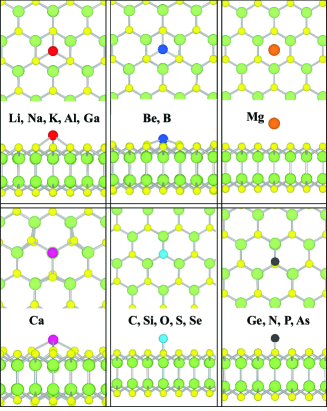
In order to explore equilibrium structures of adatom adsorbed to GaX systems, adatoms were fully relaxed on hexagonal GaX supercell and energetically most stable conformations were obtained as shown in Fig. 2 and 3. The adsorption energies of adatoms such as in the same group of Periodic Table are mostly in the same range except for O adatom. Also, adatoms from the same group of Periodic Table are adsorbed at the same adsorption site. Adsortion energies and structural parameters are listed in Table I and II. The adsorption energy values show that all these adatoms can chemically adsorb on GaS or GaSe sheets and strongly bind to the monolayers except for Mg atom. Mg shows lowest Eads values on GaX monolayers however it is not surprising due to weak bonding nature of Mg atom with early 3d transition metals [shin]. However, O atom shows the highest Eads value on GaX monolayers and it is followed by As atom. Alkali metal atoms also shows high Eads values relatively.
The binding energy for the H site, illustrated in Fig. 2, is found to be minimum for Li, Na, K, Al, Ga, Be, B and Mg atoms adsorbed to GaS monolayer. Geometric structure of B and Be atom is shown separately from the figure of Li,Na,K,Al and Ga adsorption, because B and Be are much closer than which of those and similarly Mg atom yields high distance compare with other H site adsorption figures therefore we figured that in a different column. Among 2A group adatom, Ca prefers bind to Ga top site which is different from Be and Mg atoms which prefer bind over H site. Since Ca atom pushes the closer S atom outward and Ga atom downward direction, Ca deforms the hexagon ring of GaX monolayers. While C, Si, O, S and Se atoms attach to the substrate onto S site directly, Ge, N, P and As atoms do not bind to S site exactly vertical, in other words they a little bit oriented to the B site but much more closer to the S site. Moreover they do not cause any significant deformation which is shown in Fig. 2 separately.
It is also realized that the adatoms in the third period of periodic table have smaller adsorption energies than second and fourth period of adatoms except for S adatom. For example the third period of Si adatom adsorption energy (1.22 eV) is lower than the second and fourth period of adatoms C (1.86 eV) and Ge (2.57 eV), respectively.
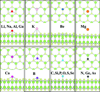
Adsorption geometries of GaSe substrates are illustrated in Fig. 3. Most of adatoms prefer same adsorption site of which GaS monolayer except for K and Be atoms. While only the Ca adatom prefers to adsorb at Ga site on GaS substrate, both Ca and K adatoms prefer to adsorb at top Ga site on GaSe substrate among the chosen atoms in this study. Similar situations are obtained for adatoms on GaSe substrates, such as the same group elements preserve the same adsorption sites and the adsorption energy of second period of periodic table smaller than the third and fourth period except for S atoms. 1A, 3A groups of adatoms are adsorbed on H site, while 4A, 5A and 6A groups of adatoms are adsorbed on Se site. Apart from all these, as in the case of adatoms on GaS substrates, all adatoms stayed above the upper layer of GaSe sheet except for Be. As an exception, the Be adatom by itself is implemented into the GaSe sheets by pushing the nearest Se atoms upper planes and one Ga atom inside so forms strong bonds with substrate atoms.
IV.2 Electronic and Magnetic Properties
In this section, we pay main attention to the electronic and magnetic properties of adatom+substrate systems for their stable structures since adsorption of adatoms can modify the electronic and magnetic properties of GaS and GaSe structures. In general, adatom adsorption on substrate is expected to alter the Fermi level, and there can be a large change in work function relative to isolated structure. We define the work function as;
where defined as the energy required to extract an electron from Fermi level to the vacuum level, Evac is determined the vacuum energy from the adatom+substrate system in the z-direction and EF is the Fermi energy of the system.
Work function of bare GaS and GaSe supercells are obtained as 6.17 eV and 5.76 eV respectively. This result is reasonable since the linear relationship between work function and ionization energy (S atom has higher ionization energy than Se atom). Results of adsorbed systems are listed in Table LABEL:tableS and LABEL:tableSe, and these results are useful to indicate the trend in for different adsorbed atoms systematically. As expected, work function for each adatom on GaX substrates are directly proportional with the ionization energy. When nonmetal adatoms are adsorbed on GaX substrate, does not change so much compared with the bare GaX systems, however in the case of alkali and poor metals, also alkali earth metals, values decrease compared with the bare GaX structures.
We observed that magnetism can be induced in GaS and GaSe sheets by only the group 4A and 5A non-metallic atoms (also by poor-metal Ge) adsorption. The C, Si, Ge, N, P, As adsorbed GaS and GaSe sheets favor the spin-polarized states as seen from the results given in Table 1 and 2. Group 4A adatom C, Si, Ge adsorbed systems have larger magnetic moment of 2 than group 5A adatoms N, P, As adsorbed systems which have a value of 1 for both GaS and GaSe sheets.
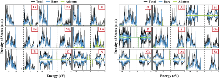
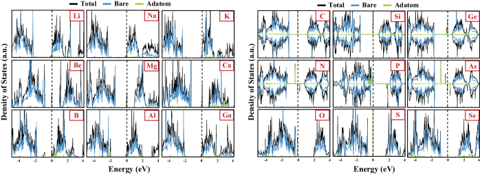
Density of states (DOS) of each adatom adsorbed to GaS and GaSe monolayer on the favored adsorption sites are presented in Fig. 4 and 5, respectively. The present analysis uses a scheme to deduce the effects of adsorption, such that both figures included the DOS of the ”bare” extended substrate, the total and projected densities of states (PDOS) of adatom to find out the energy shifts of adatom localized states relative to the ”bare” extended substrate.
The DOS related with the single adatom adsorbed to GaS substrate are illustrated in Fig. 4. We start to DOS analysis with alkali metal adsorption (Li, Na, K) on GaS substrate. These adatoms donate a part of their valance charge to the states which overlaps with the bottom of the conduction band of the extended substrate. However, both minimum of the conduction and maximum of the valance band are shifted downward direction and all of the structures are still large gap semiconductor. Unlike the elements group 1A alkali metals, alkali earth metals (Be, Mg and Ca) significantly alter the GaS electronic structure. An important common feature in the DOS for these adatoms on GaS is the hybridization of the adatom and GaS states which is evident from prominent peaks in the DOS as shown in Fig. 4. The impurity states occur inside the gap of extended substrate, so the gap is reduced compared to bare structure. Adatoms from group 3A display similar situation with group 1A adatoms except for B atom, since the electronic structure of B adsorbed to GaS sheet turns to metallic. The impurity states occur very close to the Fermi level and cross each other near to the Fermi level. States derived from C, Si, and Ge adatoms adsorbed to GaS are spin-polarized and appear near the Fermi level. Spin-up states occur below the Fermi level and hence become occupied. Similar characteristics for the DOS are found for group 5A adatoms (N, P, As), however energy levels of both these group adatoms are splitted to spin-up and spin-down channels resulting a net magnetic moment. For the case N adsorption to the GaS substrate, two spin-up impurity states are occupied at the -0.36 and -0.92 eV below the Fermi level, while in the spin-down channel, one of the impurity state is occupied at the -0.1 eV below the Fermi level and the other one is empty at the 0.42 eV above the Fermi level. P and As adatom display similar situation like N adatom, therefore the fundamental band gap of structure is locally reduced for these adatoms. We now discuss the DOS for O adatom which is representative of group 6A adatoms S and Se. O derived states occur in the valance band, however, S and Se adatom derived states occur in conduction band but low in intensity. Nevertheless, these adatoms adsorbed to GaS substrate preserve the fundamental wide band gap as semiconducting in electronic property. The DOS figures related with single adatom adsorbed to GaSe substrate are illustrated in Fig. 5. Comparing with Fig. 5 with Fig. 4, trends mentioned above are similar with corresponding adatoms with insignificant changes in electronic states.
The amount of charge accumulation is different for most of adatoms treated on GaS and GaSe sheets which are given in Table 1 and 2. Bader analysis results give that all adatoms except for S atom (also Se atom on GaSe sheet, but it is too small, so ignorable), donate charge to GaS and GaSe substrate. We assigned a negative sign to the calculated value of if charge is transferred from substrate to adatom. S atom on GaX sheets take small amount of charges from substrates. Se atom gives small amount of charge to S atom on GaS substrate because of higher electronegativity of S atom compare with Se atom, relatively. The most adatom is stabilized closer to the surface, thus ionic bonding appears and overall hexagonal geometry has been retained.
V Conclusions
In this paper, adsorption of 18 different adatoms on GaX is studied using the first principles density functional theory. Calculations of adsorption energy, geometric structure, density of states, charge transfer and work function give a consistent picture for the adatoms considered. Results show that all adatoms considered in this study chemically adsorb to GaX monolayers except for Mg atom due to weak bonding nature of Mg atom with early 3d transition metals, however O atom shows the highest Eads value on GaX monolayers. Adatoms from groups I-III on GaS substrate exhibit characteristic of ionic bonding (except for Mg) and very small distortion of the GaX sheet with a little changes in the GaX electronic states. Significant charge transfers are observed except for S and Se atoms and total magnetic moments are found by adsorption of adatoms which is essential for spintronic applications. Work function results provide useful knowledge of trend in for different adsorbed atoms systematically. Our study represents adsorption strategies of GaX monolayers therefore a theoretical knowledge for future experimental and theoretical studies.
Acknowledgements.
We would like thank to TUBITAK ULAKBIM, High Performance and Grid Computing Center for numerical calculations. H. D. O. and E. A. acknowledge support from TUBITAK through the project No. 116F059.References
- [1] Xiang Yuan, Lei Tang, Shanshan Liu, Peng Wang, Zhigang Chen, Cheng Zhang, Yanwen Liu, Weiyi Wang, Yichao Zou, Cong Liu, et al. Arrayed van der waals vertical heterostructures based on 2d gase grown by molecular beam epitaxy. arXiv preprint arXiv:1601.02317, 2016.
- [2] Xufan Li, Ming-Wei Lin, Alexander A Puretzky, Juan C Idrobo, Cheng Ma, Miaofang Chi, Mina Yoon, Christopher M Rouleau, Ivan I Kravchenko, David B Geohegan, et al. Controlled vapor phase growth of single crystalline, two-dimensional gase crystals with high photoresponse. Scientific reports, 4:5497, 2014.
- [3] Masoud Mahjouri-Samani, Mengkun Tian, Kai Wang, Abdelaziz Boulesbaa, Christopher M Rouleau, Alexander A Puretzky, Michael A McGuire, Bernadeta R Srijanto, Kai Xiao, Gyula Eres, et al. Digital transfer growth of patterned 2d metal chalcogenides by confined nanoparticle evaporation. ACS nano, 8(11):11567–11575, 2014.
- [4] Mingsheng Xu, Tao Liang, Minmin Shi, and Hongzheng Chen. Graphene-like two-dimensional materials. Chemical reviews, 113(5):3766–3798, 2013.
- [5] PingAn Hu, Zhenzhong Wen, Lifeng Wang, Pingheng Tan, and Kai Xiao. Synthesis of few-layer gase nanosheets for high performance photodetectors. ACS nano, 6(7):5988–5994, 2012.
- [6] M Yagmurcukardes, RT Senger, FM Peeters, and H Sahin. Mechanical properties of monolayer gas and gase crystals. Physical Review B, 94(24):245407, 2016.
- [7] L. Leontie, I. Evtodiev, V. Nedeff, M. Stamate, and M. Caraman. Photoelectric properties of bi2o3/gase heterojunctions. Applied Physics Letters, 94:071903, 2009.
- [8] Wei Shi, J. Ding Yujie, Nils Fernelius, and Konstantin Vodopyanov. Efficient, tunable, and coherent 0.18-5.27-thz source based on gase crystal. Optics Letters, 27(16):1454–1456, 2002.
- [9] K. R. Allakhverdiev and M. Ö. Yetis. Effective nonlinear gase crystal. optical properties and applications. Laser Physics, 19(5):1092–1104, 2009.
- [10] N. M. Gasanly, A. Aydınlı, H Özkan, and C. Kocabas. Temperature dependence of the first-order raman scattering in gas layered crystals. Solid State Communications, 116(3):147–151, 2000.
- [11] Mustafa Yüksek, Hüseyin Ertap, Ayhan Elmali, H. Gul Yaglioglu, Gasan M. Mamedov, Mevlüt Karabulut, and Mustafa K. Öztürk. Two photon absorption characteristics of bulk gate crystal. Optics and Laser Technology, 44(7):2178–2181, 2012.
- [12] Dattatray J Late, Bin Liu, Jiajun Luo, Aiming Yan, HSS Matte, Matthew Grayson, CNR Rao, and Vinayak P Dravid. Gas and gase ultrathin layer transistors. Advanced Materials, 24(26):3549–3554, 2012.
- [13] Dattatray J Late, Bin Liu, HSS Matte, CNR Rao, and Vinayak P Dravid. Rapid characterization of ultrathin layers of chalcogenides on sio2/si substrates. Advanced Functional Materials, 22(9):1894–1905, 2012.
- [14] Sidong Lei, Liehui Ge, Zheng Liu, Sina Najmaei, Gang Shi, Ge You, Jun Lou, Robert Vajtai, and Pulickel M Ajayan. Synthesis and photoresponse of large gase atomic layers. Nano letters, 13(6):2777–2781, 2013.
- [15] C Lévy-Clément, R Tenne, and A Aruchamy. Photoelectrochemistry and photovoltaics of layered semiconductors. 1992.
- [16] Chan Su Jung, Fazel Shojaei, Kidong Park, Jin Young Oh, Hyung Soon Im, Dong Myung Jang, Jeunghee Park, and Hong Seok Kang. Red-to-ultraviolet emission tuning of two-dimensional gallium sulfide/selenide. ACS nano, 9(10):9585–9593, 2015.
- [17] Shengxue Yang, Qu Yue, Hui Cai, Kedi Wu, Chengbao Jiang, and Sefaattin Tongay. Highly efficient gas molecule-tunable few-layer gase phototransistors. Journal of Materials Chemistry C, 4(2):248–253, 2016.
- [18] Shengxue Yang, Yan Li, Xiaozhou Wang, Nengjie Huo, Jian-Bai Xia, Shu-Shen Li, and Jingbo Li. High performance few-layer gas photodetector and its unique photo-response in different gas environments. Nanoscale, 6(5):2582–2587, 2014.
- [19] Xufan Li, Leonardo Basile, Bing Huang, Cheng Ma, Jaekwang Lee, Ivan V Vlassiouk, Alexander A Puretzky, Ming-Wei Lin, Mina Yoon, Miaofang Chi, et al. Van der waals epitaxial growth of two-dimensional single-crystalline gase domains on graphene. ACS nano, 9(8):8078–8088, 2015.
- [20] Yan Li, Hui Chen, Le Huang, and Jingbo Li. Ab initio study of the dielectric and electronic properties of multilayer gas films. The journal of physical chemistry letters, 6(6):1059–1064, 2015.
- [21] Yandong Ma, Ying Dai, Meng Guo, Lin Yu, and Baibiao Huang. Tunable electronic and dielectric behavior of gas and gase monolayers. Physical Chemistry Chemical Physics, 15(19):7098–7105, 2013.
- [22] Yuting Peng, Congxin Xia, Heng Zhang, Tianxing Wang, Shuyi Wei, and Yu Jia. Characteristics of p-type mg-doped gas and gase nanosheets. Physical Chemistry Chemical Physics, 16(35):18799–18804, 2014.
- [23] Sianxin Wu, Xia Dai, Hongyi Yu, Heng Fan, Jiangping Hu, and Wang Yao. Magnetisms in -type monolayer gallium chalcogenides (gase, gas). arXiv preprint arXiv:1409.4733, 2014.
- [24] Ting Cao, Zhenglu Li, and Steven G Louie. Tunable magnetism and half-metallicity in hole-doped monolayer gase. Physical review letters, 114(23):236602, 2015.
- [25] L Ao, HY Xiao, X Xiang, S Li, KZ Liu, H Huang, and XT Zu. Functionalization of a gase monolayer by vacancy and chemical element doping. Physical Chemistry Chemical Physics, 17(16):10737–10748, 2015.
- [26] Hui Chen, Yan Li, Le Huang, and Jingbo Li. Influential electronic and magnetic properties of the gallium sulfide monolayer by substitutional doping. The Journal of Physical Chemistry C, 119(52):29148–29156, 2015.
- [27] W. Kohn and L. J. Sham. Self-consistent equations including exchange and correlation effects. Phys. Rev., 140:A1133–A1138, Nov 1965.
- [28] Peter E Blöchl. Projector augmented-wave method. Physical review B, 50(24):17953, 1994.
- [29] John P Perdew, Kieron Burke, and Matthias Ernzerhof. Generalized gradient approximation made simple. Physical review letters, 77(18):3865, 1996.
- [30] Stefan Grimme. Semiempirical gga-type density functional constructed with a long-range dispersion correction. Journal of computational chemistry, 27(15):1787–1799, 2006.
- [31] Jochen Heyd, Gustavo E Scuseria, and Matthias Ernzerhof. Hybrid functionals based on a screened coulomb potential. The Journal of Chemical Physics, 118(18):8207–8215, 2003.
- [32] Jochen Heyd, Gustavo E Scuseria, and Matthias Ernzerhof. Erratum:“hybrid functionals based on a screened coulomb potential”[j. chem. phys. 118, 8207 (2003)]. The Journal of Chemical Physics, 124(21):219906, 2006.
- [33] Joachim Paier, Martijn Marsman, K Hummer, Georg Kresse, Iann C Gerber, and János G Ángyán. Screened hybrid density functionals applied to solids. The Journal of chemical physics, 124(15):154709, 2006.
- [34] Georg Kresse and Jürgen Furthmüller. Efficiency of ab-initio total energy calculations for metals and semiconductors using a plane-wave basis set. Comp. Mat. Sci., 6(1):15–50, 1996.
- [35] G. Kresse and J. Furthmüller. Efficient iterative schemes for ab initio total-energy calculations using a plane-wave basis set. Phys. Rev. B, 54:11169–11186, Oct 1996.
- [36] Graeme Henkelman, Andri Arnaldsson, and Hannes Jónsson. A fast and robust algorithm for bader decomposition of charge density. Comp. Mat. Sci., 36(3):354–360, 2006.