Electronic and magnetic properties of the graphene densely decorated with 3d metallic adatoms
Abstract
The electronic properties of graphene decorated with Ni, Co, Cu and Zn adatoms is studied with the density functional theory approach. Within the analysis the spin-orbit interaction is taken into account. We focus on the case when the indicated metallic adatoms form a perfect, close-packed single-atomic layer above the graphene surface. The two configurations are examined, namely the adatoms in the on-top, and the hollow positions on graphene. First, we verify that the metallic adatoms in the close-packed structure do not form a covalent bonds with the graphene substrate. However, due to the proximity of the metallic adatoms to the graphene, the charge transfer from the adatom layer to the graphene takes place, and in consequence the graphene becomes -doped. The observed charge transfer results from the arising hybridization between the graphene and transition metal orbitals. The proximity of metallic adatoms modifies the magnetic state of the graphene. This effect is especially pronounced for the decoration with magnetic atoms, when the magnetic moments on the graphene sublattices are induced. The analysis of the band structure demonstrates that the charge transfer, as well as the induced magnetism on graphene, modify the graphene electronic properties near high symmetry points, especially the Dirac cones. The presence of the metallic adatoms breaks graphene symmetry and splits the bands due to the exchange coupling. We show that for the hollow configuration the gap opening arises at the -point due to the Rashba-like spin-orbit interaction, while in the case of the on-top configuration the energy gap opens mainly due to the staggered potential. We also mapped the parameters of an effective Hamiltonian on the results obtained with the density functional theory approach.
1 Introduction
Graphene is one of the most prominent currently studied two dimensional material [1]. This stable single layer of carbon atoms forms a honeycomb lattice and possesses extraordinary electronic properties, i.e. a linear band dispersion for low energies near and symmetry points. The exciting electronic properties of graphene originate from the fact that its structure consists of the two equivalent sublattices, with the assigned pseudospins [2, 3, 4].
Since it is technologically inconvenient to obtain free standing graphene and incorporate it into electronic devices, the graphene growth on various substrates, as well as its decoration with various adatoms, or formation of the hetero-layered structures addresses much attention [5]-[20]. The structural incorporation of graphene with other materials may lead to the enhancement of the spin-orbit interaction, which destroys the perfect massless-relativistic picture for charge carriers and introduces the gap in the energy spectrum as well as a spin-splitting of the bands. This feature is desirable, if addressing the graphene as a part of the electronic devices for spin-dependent transport, spin-filtering and magnetic valves. On the other hand, the unbounding of the graphene from substrates, e.g. by intercalation, in order to recapture its unique relativistic properties is also desirable.
The magnitude of the intrinsic spin-orbit coupling in pristine graphene is small – of orders of tens – and originates from the graphene -orbitals hybridization [27]. Therefore, a scientific effort is done to study the rôle of substrate or decoration with adatoms. First theoretical and experimental works analyzed the rôle of the metallic substrate on the electronic properties of graphene [21]-[26], however the relativistic effects were not taken into account in those studies. Recently, several theoretical works appeared considering quantitatively the influence of the spin-orbit interaction on the symmetry breaking near , points and its influence on the modification of the linear dispersion of the Dirac cone for the graphene placed on the metallic surfaces [28, 29, 30, 31, 32]. The properties of grahene decorated with metallic adatoms was also discussed [33].
In this paper we focus on how the electronic properties of the graphene are modified when the graphene is decorated with a single layer of the close-packed metallic adatoms. The paper is organized as follows. First, the considered structures and applied methods are described. Next, taking into account the spin-orbit interaction as implemented in the applied pseudopotential DFT method, the general electronic properties, regarding charge transfer and the modification of the band structure of the graphene in the proximity of the metallic layer are considered. Subsequently, the insight into the orbital hybridization between the graphene and the metallic layer is presented. Then, the proximity induced magnetism on graphene is described. In the end, the quantitative analysis of the influence of the spin-orbit interaction of the Rashba-like type, the exchange coupling and the staggered potential at the Dirac point of the specified heterostuctures is presented and discussed.
2 Method and System Geometry
The presented results were obtained using a DFT approach as implemented in the plane-wave pseudopotential Quantum Espresso code [34]. We used fully-relativistic pseudopotentials in the Perdew-Burke-Ernzerhof (PBE) parametrization for the exchange–correlation functional [35]. A plane-wave energy cutoff was set to 80 Ry, while charge density cutoff to 600 Ry, for all atomic species. The applied pseudopotntials contain the , projections of valence states for carbon atoms, while , and projections for metallic adatoms. Within the analysis the Hubbard corrections for the adatomic orbitals, in rotationally invariant scheme, were taken into account [36]. The value of the effective parameter for the nickel was set to eV, while for the cobalt and zinc we assumed eV [37], and for copper we set eV. We also took into account the semi–empirical van der Waals corrections, since they are important for the large systems with dispersion forces [38, 39].
The considered hexagonal supercells consists of the two graphene atoms, of A and B sublattices, and the metallic adatom in the on-top or hollow positions. The geometries of the considered structures with indicated supercellls are presented in Fig.1. The periodic slabs were separated by 12 Å of vacuum. We used a uniform 30301 Monkhorst-Pack k-mesh [40] to sample the first Brillouin zone for the hexagonal supercells. Within the applied parameters and pseudopotentials, the optimized C–C distance of pristine graphene is 1.42 Å.
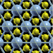
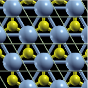
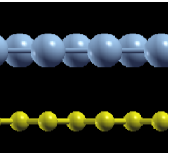
Since we focus on the close-packed decoration, the choice of the specified adatoms is motivated by the adequate matching of the lattice constants of graphene and the lattice constants of the established metallic layers. We focus on the studies of decoration with nickel and copper atoms, since the Ni–Ni interactomic distance on the Ni(111) surface is 2.48 Å and the Cu–Cu interatomic distance on Cu(111) surface is 2.55 Å, as well as with cobalt and zinc atoms, since the interatomic distances for the Co(0001) and Zn(0001) close-packed surfaces are 2.51 Å and Zn–Zn 2.66 Å, respectively [41, 42]. The optimized distances between the graphene and the close-packed adatomic layers are given in Tab.1. The presented values suggest the physisorbtion of the metallic adatoms on the graphene substrate. This statement is then confirmed by the analysis of the binding energy calculated per grahene C–atom. The values of the binding energy, presented in Tab.3, are far lower than 500 meV, what allows us to conclude that no covalent bounds are formed between the graphene and the close-packed adatoms.
| Ni(h) | Ni(t) | Co(h) | Co(t) | Cu(h) | Cu(t) | Zn(h) | Zn(t) | |
| d | 3.3754 | 3.0648 | 3.2112 | 3.1218 | 3.0787 | 3.1011 | 3.4636 | 3.3154 |
The values of the total energy for the graphene with metallic adatoms is shown in Tab.2. From the analysis of the total energies in the specific configurations it is clearly seen, that the on-top configuration is the preferred one for nickel and cobalt layers, namely for the ferromagnetic metallic layers. The difference in total energy between the hollow and on-top configurations is of order of 14 and 20 meV for the nickel and cobalt layers, respectively. This suggests that, while close-packed, the mentioned atoms do not tend to nest the hollow position on the graphne lattice and rather be imbedded in the on-top position. The difference of the total energies for the copper layers is of order of few eV merely, in favor of the on-top configuration, while the zinc atoms prefer to nest the hollow position, and the difference between the total energy in the on-top and hollow configurations for the latter adatom species is found to be equal 2.5 meV.
At this point we emphasize however, that supercell we applied to our DFT analysis is too small to include the effects of the Moire patterns of the graphene–metal interface [43, 44, 45, 46], as well as the buckled graphene patterns [47]. Hence, the analysis of the spatially extended system, with larger supercells, could led us to different conclusions regarding the structure privileges. Moreover, we verified that the reduction by half of the adatoms concentration on the graphene significantly changes the bonding type. Namely, when the adatoms are spread on graphene at lower concentrations they tend to form covalent bonds with the graphene substarate.
| Ni | Co | Cu | Zn | |
|---|---|---|---|---|
| on-top | -124.29904316 | -99.88880617 | -141.30003430 | -172.23111898 |
| hollow | -124.29798240 | -99.88733592 | -141.30002475 | -172.23130580 |
| Ni | Co | Cu | Zn | |
|---|---|---|---|---|
| on-top | 133.34 | 107.66 | 62.82 | 103.94 |
| hollow | 117.45 | 87.74 | 62.69 | 106.49 |
3 Results
3.1 Band structure
In order to verify the results with spin-orbit coupling, first we calculated the intrinsic spin-orbit induced gap for pristine graphene at the K-point. With the established DFT parameters, supercells and pseudopotentials we obtained value of the intrinsic spin-orbit gap at 10 . This value stays in excellent agreement with the previous DFT results [48] and also gives a precision of our spin-orbit induced energy gap calculations that are presented in the final part of this work.
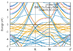
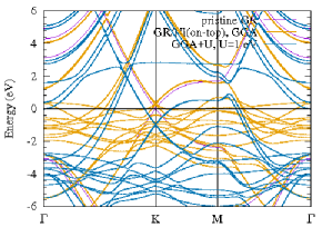
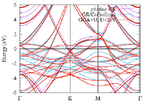
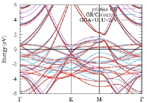
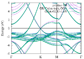
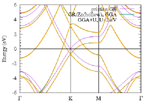
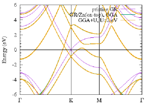
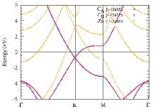
In Fig.2, the band structures for the graphene densely decorated with metallic adatoms for the hollow and the on-top positions are shown. In the on-top case the metallic adatom is situated above the graphene carbon atom of the A sublattice, hence a coupling with the A sublattice is assumed to be stronger than with the B sublattice. For the hollow configuration the equal couplings with both sublattices are present. The adatom type and position on the graphene lattice is indicated in the figure. The band structure for the pristine graphene is plotted with the purple line and presented in all figures for compartion. The figures show the course of the band structures obtained in the calculations where the Hubbard corrections of the metallic orbitals are or are not taken into account, as indicated. For the presented energy range, there is no much difference in the band structure between the hollow and the on-top configurations along reciprocal path for the particular considered adatomic layer. The exception is the vicinity of the -point, where the difference in the band structure for the conduction states between the hollow and the on-top cases is pronounced. This difference is especially pronounced for Ni, Co and Cu adatomic layers around 2 eV, and appears despite the treat of the Hubbard corrections. The difference in the band structure course near the -point is attributed to the fact that for the on-top configuration the symmetry breaking appears in the reciprocal space near -point on – path.
At the presented energy range, the linear dispersion near symmetry point is reproduced for all considered adatoms. However, the shift in energy of the Dirac point with respect to the Fermi Energy , here denoted by , appears. We attribute this shift to the strength and type of the hybridization between the graphene and adatomic layer. The -doping type is observed for all studied adatoms, since the Dirac point of the considered systems is shifted below the Fermi energy. It is worth to underline, that taking into account the Hubbard corrections in the case of nickel layer is crucial, since it alters the graphne doping type, while for the zinc adatomic layer the modification in the course of the band structure introduced by the Hubbard correction is unnoticeable in the presented energy range, despite the assumption of a quite large value of the parameter. In general, the two groups of the adatoms among the studied ones may be distinguished. There are the adatoms that tend to hybridize strongly with the graphene, and for them the shift of the Dirac point is significant – these are nickel, cobalt and zinc, and the adatoms that can be regarded as weakly coupled to the graphene – the copper. The values of the shift in energy of the Dirac point for all considered adatoms are presented in Tab.4. Our observation of the graphene doping type stays in agreement with the previous studies of the graphene placed on the metallic substrates [26, 49].
| Ni | Co | Cu | Zn | |
|---|---|---|---|---|
| on-top | -0.9710 | -0.5869 | -0.1425 | -0.9059 |
| hollow | -0.9824 | -0.3329 | -0.1718 | -0.7170 |
One may also observe, that the set of flat doping bands builds up below or/and around the Fermi energy. The position and spread in energy of the set of the doping bands depends on the adatom type. For the presented energy window the set of doping bands is clearly visible for the nickel, cobalt and copper adatomic layers, while for the zinc the doping bands lay below the presented energy frame. Importantly, for the nickel and cobalt adatoms, and lesser for the copper layer, the location in energy of the doping bands depends on the strength of the Hubbard corrections. In general, taking into account the Hubbard corrections results in dragging down in energy of the valence bands, while the conduction states are less affected by these corrections. In the case of nickel, cobalt and to some extend copper, the increase of the correlations enhances the shifting down the doping bands. As mentioned above, the inclusion of the Hubbard correction not only influences the position of the doping bands, but also the position in energy of the Dirac point. Here, the two types of the adatoms may be extracted. The adatoms for which the Hubbard correction notably shifts down the Dirac point and/or the position of the doping bands – for this group the adatoms forming the ferromagnetic layers, namely nickel and cobalt atoms are included. The other group consists of the adatoms, for which the Hubbard corrections do not influence the position of the Dirac point and the doping bands are merely moved. The later group represents the copper and zinc, namely nonmagnetic adatoms.
The effect responsible for the shifting down the band structure, and in particular, the Dirac point below the Fermi energy is the charge transfer that takes place from the metallic layer to the graphene. This charge transfer is possible since the hybridization between the specific graphene and adatomic layer orbitals develops. The -type doping for graphene on metallic surfaces is predicted theoretically [28, 22] and reported in experiment [50].

3.2 The hybridization
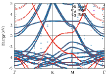
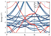
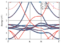
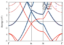
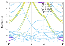
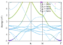
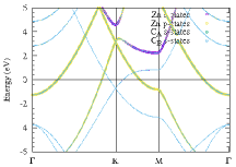
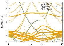
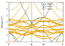
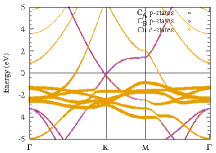
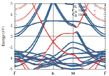
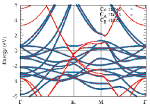
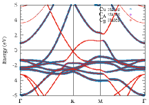
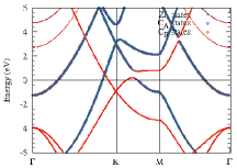
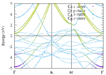
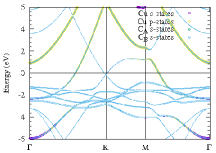
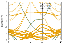
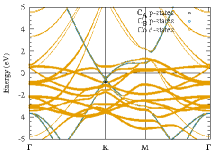
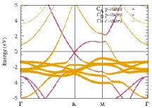
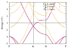
The analysis of the adatomic layer – graphene hybridization for the hollow and the on-top configurations is presented in Fig.3 and Fig.4, respectively. The left panel of these figures shows the band structure projected on the indicated atoms of the considered supercells. The provenance of the build-in flat doping bands, the modification of the graphene-based bands, as well as the crossings and anti-crossings between the adatomic and graphene states in the reciprocal space are visible. The middle panels of Fig.3 and Fig.4 show the band structures projected on the adatomic 3 and 3, as well as the graphene 2 states, while the right panels show the projections on the adatomic 3 and graphene 2 states. In the case of the nickel, copper and zinc layers the grapehne 2 and adatomic 3, 3 and 3 states do not constitute the graphene cone. For the mentioned layers the graphene cone is constituted by the carbon 2 states only and the contribution from the states of the A and B sublattices is equal for the hollow configuration, while in the on-top configuration the modest difference for the states of the A and B sublattives is observed. The exeption is the cobalt layer. For the cobalt in the on-top confguration the hybridization encompasses the bands forming the Dirac cone. The flat doping bands originate from the adatomic 3 states. For the cobalt layer these states are also found at the energy range where the Dirac point is located, and for the conduction states. The hilly bands crossing the Fermi energy, that originate from the adatomic 3 states for zinc, and from adatomic 3 and 3 states for nickel, cobalt and carbon atoms, are also visible. Hence, the in-plane electron transport across the considered hybrid structure involves not only the graphene -states, or in the case of the cobalt layer – the low velocity doping states, but also the 3 states for zinc layer and 3 plus 3 states of the nickel, cobalt and copper metallic layers. This analysis provides us the information for the proper construction of an effective Hamiltonian in the charge carrier transport description, where not only the graphene 2 and adatomic (or substrate) 3 states should be taken into account, but also the 3 doping states should be included.



3.3 The magnetism induced in graphene due to the proximity of an adatomic metallic layer
Due to the proximity of the adatomic layers the finite values of the magnetic moments are induced on the graphene sublattices. The induced magnetism and its impact on the band structure depends significantly on the adatom type (whether they are magnetic or not) and the configuration on the graphene lattice.
Although the total magnetic moment of the considered supercells containing nonmagnetic adatoms is zero, we find the small values of the induced magnetic moments on the graphene as well as on the metallic adatoms, for the studied nonmagnetic metallic layers. Hence, the finite values of the exchange coupling should be taken into account while describing the system with an effective Hamiltonian. The analysis of the proposed Hamiltonian is discussed in the next part of this paper. We also notice, that the tiny induced magnetic moments on the adatoms and the graphene sublattices are oriented perpendicularly to the system surface and oriented in line.
For the ferromagnetic layers we observe that for the on-top, as well as for the hollow configurations, magnetic moments located on the adatoms and those induced on graphene, are oriented perpendicularly to the surface of the two-layered structure. However, the aligment of the magnetic moments differs for on-top and hollow configurations. In the on-top configuration, the alignment of the magnetic moments of the carbon atoms located below the adatom (let us assume it is the graphene A sublattice) is opposite to the aligment of the magnetic moments on the adatoms, while the magnetic moments induced on the other graphene sublattice – B, are aligned in the same direction as the moments on the adatoms. In the hollow configuration the aligment of the induced magnetic moments on the both graphene sublattices is opposite (cobalt) or consistent (nickel) to the direction of the magnetic moments localized on the adatoms. Hence, in the on-top configuration, the proximity of the adatomic layer causes the anti-ferromagnetic aliment on the graphene sublattices, while in the hollow configuration the ferromagnetic alignment on the graphene sublattices is forced by the proximity of the localized magnetic moment, that equally couples to both graphene sublattices.
The values of the magnetic moments located on the specified magnetic atoms for the studied structures are presented in Tab.5. The proximity of all studied adatomic layer causes the exchange splitting of the graphene bands. This splitting is pronouced for the ferromagnetic adatomic layers and influences the electronic properties of the system. The exchange coupling and resulting magnetic splitting effect is particularly important in analyzing the band structure landscape near the Dirac point.
| Ni | CA (Ni) | CB (Ni) | Co | CA(Co) | CB(Co) | |
|---|---|---|---|---|---|---|
| on-top | 1.0521 | -0.0031 | 0.0012 | 1.8458 | -0.0069 | 0.0067 |
| hollow | 1.0503 | 0.0045 | 0.0045 | 1.9232 | -0.0008 | -0.0008 |
3.4 Energy dispersion in the vicinity of the Dirac point
In the case of the proximity of the metallic layer to the graphene, the electronic properties near the Dirac point can be mapped on the following effective Hamiltonian [31, 32]
| (1) |
where describes the kinetic energy of the charge carriers, with and dentoting the components of the charge carrier wave function, and , denote the Pauli matrices, while stands for the electron velocity at the Dirac point and allows to distinguish between the points. This term refers to the gapless Dirac states near points. The proximity of the metallic layer to the graphene results in symmetry beaking of the pseudospins attributed to the graphene sublattices and the formation of the staggered potential that is felt by the pseudospins. This symmetry beaking results in formation an energy gap of the width 2 at the Dirac point, and can be described with the Hamiltonian , where the , denotes the unit matrix in the spin-space, while denotes the Pauli matrix. The proximity exchange effects are then described by the Hamiltonian [31]
| (2) |
with the and being the exchange coupling constants (in the sense of the magnetic exchange coupling constants) for the indicated graphene sublattice. We notice, that in the hollow configuration, for the adatoms equally coupled to both graphene sublattices . For the on-top configuration, when the coupling to one of the graphene sublattices (let us assume A) is much stronger in comparsion to the coupling with the other subllatice, .
Finaly, the proximity effect may lead to the enhancement of the Rashba-like interaction on the graphene, hence one should also take into account the term [32]
| (3) |
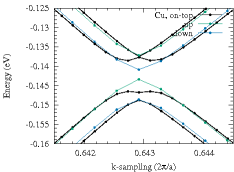
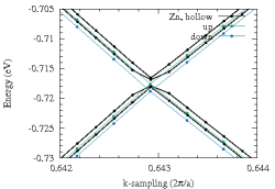
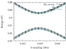
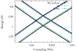
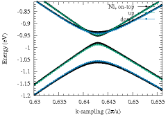
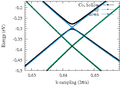
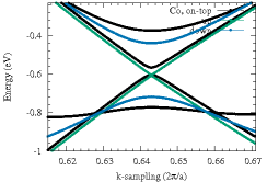
The mapping of the described effective Hamiltonian on the DFT analysis, given in allows us to extract the parameters, that are gathered in Tab.6.
| Cu(t) | 7.885 | 1.973 | 0.159 | 1.6 |
|---|---|---|---|---|
| Cu(h) | – | 1.829 | -1.849 | 1.8 |
| Zn(t) | 19.663 | 1.726 | 1.367 | 1.5 |
| Zn(h) | – | 0.228 | -0.208 | 0.2 |
| Ni(t) | 29.534 | 60.820 | 8.907 | 4.9 |
| Ni(h) | – | -49.287 | 50.460 | 4.6 |
| Co(t) | 53.751 | 72.654 | 4.732 | 5.3 |
| Co(h) | – | 67.853 | -71.224 | 5.0 |
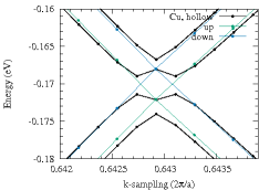
The band structures near the Dirac point for the graphene in the proximity of the copper and zinc metallic layers are presented in Fig.5. The general feature can be seen, namely, due to the staggered potential in the on-top configuration the energy gap at the is formed for all studied adatomic layers and this energy gap is additionaly widen by the Rashba-like interaction. On the other hand, for the hollow configuration the energy gap at the results from the spin-orbit coupling only. This is clearly seen when comparing the band structures at the point for the case when the spin-orbit interaction is included in the DFT calculation, with the case when calculations are performed assuming only spin-polarized system.
4 Conclusions
Within this work we studied the electronic and magnetic properties of the two-layered structure, namely when the graphene is decorated densely with the metallic adatoms. We found that no covalent bonds are formed between the graphene carbon atoms and the metallic adatoms for the perfect dense decoration. The -type doping of the graphene is found for all studied cases and is caused by the charge transfer from the metallic layer to the graphene. This charge transfer involves the orbital hybridization of the graphene states and as well as states of the adatomic layer. The two types of the adatomic layers may be distinguished among the studied layers, namely the adatoms that interact strongly with the graphene (nickel, cobalt and zinc) and those which interact weakly – copper. The proximity of the metallic layer leads to the modification of the graphene electronic properties not only via the graphene charge doping but also through the exchange coupling arising between the graphene and metallic layers, the shape of the staggered potential and the spin-orbit Rashba-like interaction. The exchange coupling is pronauced for the ferromagnetic layers, however we find the small finite values of the exchange coupling also for the nonmagnetic layers. We show that the proximity effect visibly modifies the Dirac cone and this modification depends on the adatomic configuration, namely if the adatom is coupled equally to both graphene sublattices (hollow) or the coupling with one of the sublattices dominates (on-top). In the case of the on-top as well as hollow configurations the band spin-splitting arises due to the exchange coupling of the graphene and the metallic layer. This spin-splitting is of the the order of magnitude larger for the ferromagnetic layers than for the non-magnetic layers. Additionally, for the on-top configuration the energy gap apprears, due to the staggered potential. This energy gap is then modified by the spin-orbit Rashba-like interaction, although this modification is insignificant in comparsion to the value of the gap. On the other hand, for the hollow configuration, that Rashba-like interaction introduces the energy gap at the Dirac point, since the contribution form the staggered potential is absent.
Acknowledgments
This work has been supported by the Polish Ministry of Science and Higher Education through a research project ’Iuventus Plus’ in years 2015-2017 (project No. 0083/IP3/2015/73). We thank Anna Dyrdał and Martin Gmitra for fruitful discussion. The ab initio calculations were performed on the Prometheus Computer in the Cyfronet Center, which is a part of the PL-Grid Infrastructure.
References
References
- [1] K.S. Novoselov, A.K. Geim, S.V.Morozov, D. Jiang, M.I. Katsnelson, I.V. Grigorieva, S.V. Dubonos and A.A. Firsov, Two-Dimensional Gas of Massless Dirac Fermions in Graphene, Nature, 438 (2005), pp. 197-200
- [2] A.H. Castro Neto, F. Guinea, N.M.R. Peres, K.S. Novoselov and A.K. Geim, The Electronic Properties of Graphene, Rev. Mod. Phys., 81 (2009), pp. 109-162
- [3] Mhairi H. Gass, Ursel Bangert, Andrew L. Bleloch, Peng Wang, Rahul R. Nair and A. K. Geim Free-Standing Graphene at Atomic Resolution Nature Nanotechnology 3, 676-681 (2008).
- [4] C.L. Kane and E.J. Mele, Quantum Spin Hall Effect in Graphene, Phys. Rev. Lett., 95 (2005) pp. 226801
- [5] X.S. Li, W.W. Cai, J.H. An, S. Kim, J. Nah, D.X. Yang, et al, Large-Area Synthesis of High-Quality and Uniform Graphene Films on Copper Foils, Science, 324 (2009), pp. 1312-1314, DOI: 10.1126/science.1171245
- [6] K.S. Kim, Y. Zhao, H. Jang, S.Y. Lee, J.M. Kim, et al., Large-scale pattern growth of graphene films for stretchable transparent electrodes, Nature, 457 (2009), pp. 706-710, DOI: 10.1038/nature07719
- [7] A. Reina, X.T. Jia, J. Ho, D. Nezich, H.B. Son, V. Bulovic, M.S. Dresselhaus, J. Kong, Large Area, Few-Layer Graphene Films on Arbitrary Substrates by Chemical Vapor Deposition, Nano Lett., 9 (2009), pp. 30-35, DOI: 10.1021/nl801827v
- [8] J.H. Chen, C. Jang, S.D. Xiao, M. Ishigami, M.S. Fuhrer, Intrinsic and extrinsic performance limits of graphene devices on SiO2, Nature Nanotechnology, 3 (2008), pp. 206-209, DOI: 10.1038/nnano.2008.58
- [9] P.W. Sutter, J.I. Flege, E.A. Sutter, Epitaxial graphene on ruthenium, 7 (2008), pp. 406-411, DOI: 10.1038/nmat2166
- [10] S.Y. Zhou, G.H. Gweon, A.V. Fedorov, P.N. First, W.A. De Heer, D.H. Lee, F. Guinea, A.H. Castro Neto, A. Lanzara, Substrate-induced bandgap opening in epitaxial graphene, Nature Materials, (2007) pp. 770-775, DOI: 10.1038/nmat2003
- [11] C.R. Dean, A.F. Young, I. Meric, C. Lee, L. Wang, S. Sorgenfrei, et al., Boron nitride substrates for high-quality graphene electronics, Nature Nanotechnology, 5 (2010), pp. 722-726, DOI: 10.1038/nnano.2010.172
- [12] M. Ishigami, J.H. Chen, W.G. Cullen, M.S. Fuhrer, E.D. Williams, Nano Letters 7 (2007), pp. 1643-1648, DOI: 10.1021/nl070613a
- [13] K.T. Chan, J.B. Neaton, M.L. Cohen, First-principles study of metal adatom adsorption on graphene, Phys. Rev. B, 77 (2008), pp. 235430, DOI: 10.1103/PhysRevB.77.235430
- [14] P.O. Lehtinen, A.S. Foster, A. Ayuela, A. Krasheninnikov, K. Nordlund, R.M. Nieminen, Magnetic properties and diffusion of adatoms on a graphene sheet, Phys. REv. Lett., 91 (2003), pp. 017202, DOI: 10.1103/PhysRevLett.91.017202
- [15] C. Weeks, J. Hu, J. Alicea, M. Franz, R.Q. Wu, Engineering a Robust Quantum Spin Hall State in Graphene via Adatom Deposition, Phys. Rev. X, 1 (2011), pp. 021001, DOI: 10.1103/PhysRevX.1.021001
- [16] R. Petuya, A. Arnau, Magnetic coupling between 3d transition metal adatoms on graphene supported by metallic substrates, Carbon, 11 (2017), pp. 599-605, DOI: 10.1016/j.carbon.2017.02.027
- [17] Monolayer graphene growth on Ni(111) by low temperature chemical vapor deposition Rafik Addou, Arjun Dahal, Peter Sutter, and Matthias Batzill, Appl. Phys. Lett. 100, 021601 (2012)
- [18] Comparing Graphene Growth on Cu(111) versus Oxidized Cu(111) Stefano Gottardi,, Kathrin Muller, Luca Bignardi, Juan Carlos Moreno-Lopez, Tuan Anh Pham, Oleksii Ivashenko, Mikhail Yablonskikh, Alexei Barinov, Jonas Bjork, Petra Rudolf, and Meike Stohr, NanoLett. 2015, 15, 917−922
- [19] Quasi-freestanding graphene on Ni(111) by Cs intercalation M. Alattas and U. Schwingenschlögl, Scientific Reports 6, Article number: 26753 (2016)
- [20] P. Zhang, J. T. Li, J.W. Meng, A.Q. Jiang, J. Zhuang, X.J. Ning, Conductivity of graphene affected by metal adatoms, AIP ADVANCES, 7 (2017), pp. 035101, DOI: 10.1063/1.4977964 C
- [21] L. Gao, J.R. Guest, and N.P. Guisinger, Epitaxial Graphene on Cu(111), Nano Lett., 10 (2010), pp. 3512–3516
- [22] K. Yamamoto, M. Fukushima, T. Osaka, and C. Oshima, Charge-transfer mechanism for the (monolayer graphite)/Ni(111) system, Phys. Rev. B, 45 (1992), pp. 11358–11361
- [23] Yu. S. Dedkov, M. Fonin, Electronic and magnetic properties of the graphene–ferromagnet interface, New Juounal of Physics, 12 (2010), pp. 125004
- [24] A. Tamtogl, E. Bahn, J. Zhu, P. Fouquet, J. Ellis, and W. Allison, Graphene on Ni(111): Electronic Corrugation and Dynamics from Helium Atom Scattering, J. Phys. Chem. C, 119, (2015), pp. 25983–25990
- [25] J.A. Garlow, L. K. Barrett, L. Wu, K. Kisslinger, Y. Zhu and J. F. Pulecio, Large-Area Growth of Turbostratic Graphene on Ni(111) via Physical Vapor Deposition, SCIENTIFIC Reports — 6:19804 — DOI: 10.1038/srep198 (2015)
- [26] General Approach to understanding the electronic structure of grapnene on metals, E N Voloshina, Yu S Dedkov, Mater. Res. Expresss 1 (2014), pp. 035603
- [27] M. Gmitra, S. Konschuh, C. Ertler, C. Ambrosch-Draxl, and J. Fabian, Band-structure topologies of graphene: spin-orbit coupling effects from first principles. Phys. Rev. B, (2009), pp. 235431
- [28] T. Frank, S. Irmer, M. Gmitra, D. Kochan, and J. Fabian, Copper adatoms on graphene: Theory of orbital and spin-orbital effects Phys. Rev. B, 95 (2017), pp. 035402
- [29] Giant Rashba splitting in graphene due to hybridization with gold D. Marchenko, A. Varykhalov, M.R. Scholz, G. Bihlmayer, E.I. Rashba, A. Rybkin, A.M. Shikin and O. Rader Nature Communications 3, 1232 (2012)
- [30] Spin-split electronic states in graphene: Effects due to lattice deformation, Rashba effect, and adatoms by first principles Samir Abdelouahed, A. Ernst, and J. Henk I. V. Maznichenko, I. Mertig, Phys. Rev. B 82 (2010), pp. 125424
- [31] K. Zollner, M. Gmitra, T. Frank, and J. Fabian, Theory of proximity-induced exchange coupling in graphene on hBN/(Co, Ni), Phys. Rev. B, 94 (2016), pp. 155441, DOI: 10.1103/PhysRevB.94.155441
- [32] A. Dyrda l, J. Barnaś, Anomalous, spin, and valley Hall effects in graphene deposited on ferromagnetic substrates, 2D Mater, 4 (2017), pp. 034003
- [33] Kevin T. Chan, J. B. Neaton, and Marvin L. Cohen, First-principles study of metal adatom adsorption on graphene, PHYSICAL REVIEW B 77, 235430 (2008)
- [34] Giannozzi P, Baroni S, Bonini N, et al. (2009) QUANTUM ESPRESSO: a modular and open-source software project for quantum simulation of materials. J Phys: Condens Matter 21: 395502.
- [35] Perdew JP, Burke K, Ernzerhof M (1996) Generalized Gradient Approximation made simple. Phys Rev Lett 77: 3865–3868.
- [36] A.I. Liechtenstein, V.I. Anisimov and J. Zaane, Density-functional theory and strong interactions: Orbital ordering in Mott-Hubbard insulators, Phys. Rev. B, 52 (1995), pp. R5467
- [37] S. Selcuk and A. Selloni, DFT+U Study of the Surface Structure and Stability of Co3O4(110): Dependence on U, J. Phys. Chem. C, 119 (2015), pp. 9973–9979, DOI: 10.1021/acs.jpcc.5b02298
- [38] S. Grimme, J. Comp. Chem. 27, 1787 (2006), DOI: 10.1002/jcc.20495
- [39] V. Barone et al., J. Comp. Chem. 30, 934 (2009), DOI: 10.1002/jcc.21112
- [40] Monkhorst HD, Pack JD (1976) Special points for Brillouin-zone integrations. Phys Rev B 13: 5188–5192.
- [41] Acoustic surface phonons of graphene on Ni(111) Amjad al Taleb, Gloria Anemone, Daniel Farías, Rodolfo Miranda Volume 99, April 2016, Pages 416-422
- [42] J.E. Prieto, Ch. Rath, S. Müller, R. Miranda, K. Heinz, Surface Science 401 (1998) 248–260
- [43] Y. Murata, V. Petrova, B.B. Kappes, A. Ebnonnasir, I. Petrov, Y.-H. Xie, C. V. Ciobanu, and S. Kodambaka, Moiré Superstructures of Graphene on Faceted Nickel Islands, ACS Nano, 4 (2010), pp. 6509–6514, DOI: 10.1021/nn102446y
- [44] N. Reckinger, E. Van Hooijdonk, F. Joucken, A. V. Tyurnina, S. Lucas, J.-F. Colomer, Anomalous moiré pattern of graphene investigated by scanning tunneling microscopy: Evidence of graphene growth on oxidized Cu(111), Nano Research, 7 (2014), pp. 154–162,
- [45] Moire Superstructures of Graphene on Faceted Nickel Islands, Yuya Murata, Vania Petrova, Branden B. Kappes, Abbas Ebnonnasir, Ivan Petrov, Ya-Hong Xie, Cristian V. Ciobanu, and Suneel Kodambaka, ACS Nano VOL. 4, NO. 11, 6509–6514, 2010
- [46] Role of the Pinning Points in epitaxial Graphene Moiré Superstructures on the Pt(111) Surface, José I. Martínez, Pablo Merino, Anna L. Pinardi, Otero-Irurueta Gonzalo, María F. López, Javier Méndez and José A. Martín-Gago Scientific Reports 6, Article number: 20354 (2016)
- [47] S.Deng, V. Berry, Wrinkled, rippled and crumpled graphene: an overview of formation mechanism, electronic properties, and applications, 19 (2016), pp. 197-212 , DOI: 10.1016/j.mattod.2015.10.002
- [48] Sergej Konschuh, Martin Gmitra, and Jaroslav Fabian Phys. Rev. B 82, 245412 – Published 10 December 2010
- [49] P. A. Khomyakov, G. Giovannetti,P. C. Rusu,G. Brocks,J. van den Brink, and P. J. Kelly, First-principles study of the interaction and charge transfer between graphene and metals, PHYSICAL REVIEW B 79, 195425 2009, DOI: 10.1103/PhysRevB.79.195425
- [50] Y.Dedkov, W. Klesse, A.Becker, F. Späth, Ch. Papp, E. Voloshina, Decoupling of graphene from Ni(111) via oxygen intercalation, Carbon Volume 121, September 2017, Pages 10-16, DOI: 10.1016/j.carbon.2017.05.068