Magnetic properties, spin waves and interaction between spin excitations and 2D electrons in interface layer in Y3Fe5O12 / AlOx / GaAs-heterostructures
Abstract
We describe synthesis of submicron Y3Fe5O12 (YIG) films sputtered on GaAs-based substrates and present results of the investigation of ferromagnetic resonance (FMR), spin wave propagation and interaction between spin excitations and 2D electrons in interface layer in YIG / AlOx / GaAs-heterostructures. It is found that the contribution of the relaxation process to the FMR linewidth is about 2 % of the linewidth . At the same time, for all samples FMR linewidths are high. Sputtered YIG films have magnetic inhomogeneity, which gives the main contribution to the FMR linewidth. Transistor structures with two-dimensional electron gas (2DEG) channels in AlOx / GaAs interface governed by YIG-film spin excitations are designed. An effective influence of spin excitations on the current flowing through the GaAs 2DEG channel is observed. Light illumination results in essential changes in the FMR spectrum. It is found that an increase of the 2DEG current leads to an inverse effect, which represents essential changes in the FMR spectrum.
I Introduction
Integration of ferrites with semiconductors offers many advantages and new possibilities in microwave applications such as high-speed wireless communications, active phased array antennas for radars, astronomy systems, auto radars, space electronics and satellite navigation. This integration gives significant advantages in miniaturisation, bandwidth, speed, radio reception selectivity and the production costs of monolithic microwave integrated circuits (MMICs) Chen12 . Ferrite film growth on semiconductor substrates is very important for development of new types of spintronic and spin-wave devices such as microwave filters, delay lines, and spin-polarized field-effect transistors (spin-FET).
At present, spin-wave devices have been realized on the basis of Y3Fe5O12 (YIG) films grown on gadolinium-gallium garnet (Gd3Ga5O12, GGG) substrates Stan09 ; Kabos . Narrow-band filtration can be achieved in YIG-based one-dimensional magnonic crystals Mrucz14 ; Bes15 ; Vys17 . The pulsed laser deposition technique has been used to grow submicron YIG films on GGG substrates for microwave spin-wave band pass filter Man09 . Construction of spin-wave devices on the basis of YIG films directly deposited on semiconductors is the next stage in the development of spin-wave devices. The recent progress in synthesis of nanometer YIG films of high quality on semiconductor substrates Stog15 ; Stog15a and low relaxation of long-wavelength spin waves in nanometer magnetic films Lut12 ; Lut16 give a possibility to construct spin-wave devices on semiconductor chips operating in the microwave frequency band.
Active control and manipulation of spin degrees of freedom in spin-FET is one of the main problems in spintronics Dat90 ; Hall03 ; Schl03 ; Egues03 ; Zut04 ; Sug06 ; Crow07 ; Koo09 ; Chuang15 . The spin transport in two-dimensional electron gas (2DEG) and large spin-orbit interaction are essential for realizing spin transport devices. However, the noneffective spin injection and weak influence of the gate on electron current flowing through the transistor channel are known difficulties in spin-FET design. Modulating the channel conductance by using an electric field to induce spin precession is performed at low temperatures and has remained elusive at higher ones Koo09 ; Chuang15 . Furthermore, poor crystal quality of ferrite films sputtered on GaAs substrates has a detrimental effect on the device performance Chen12 ; Buh95 . At the same time, it needs to note that YIG films are regarded as perspective materials in spintronics SSP13 .
In this paper we describe synthesis of YIG films deposited on GaAs substrates with AlOx layers by ion-beam sputtering and present results of the characterization of YIG film / AlOx / GaAs heterostructures and their interfaces (see Sec. 2). Magnetic characteristics of deposited films are deduced from the FMR X-band spectroscopy (Sec. 3). Spin wave propagation are described in Sec. 4. In Sec. 5 we consider the influence of spin excitations in YIG films on the electron current flowing through the 2DEG channel formed at the AlOx / GaAs interface. It is found that a high interaction between spin excitations and 2DEG channel in GaAs-based substrates can be achieved at the ferromagnetic resonance (FMR) frequency of YIG films. The inverse effect, the influence of the electron current on the FMR spectrum, is described in Sec. 6. This interaction is studied by a detection of -parameters of the transistor channel at microwave frequencies under the light exposure and without light illumination. The interaction is enhanced with the light exposure of the AlOx / GaAs interface and with the microwave power increase. It is found that above the spin-wave instability threshold the increase of the 2DEG density induced by light results in essential changes in the FMR spectrum and in the -parameter of the channel.
II Sample preparation and characterization
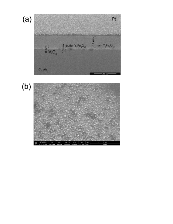
YIG films were deposited on GaAs substrates by the two-stage ion-beam sputtering in Ar + O2 atmosphere Stog92 ; Nip12 . The -GaAs substrates with thickness of 0.4 mm had the (100)-orientation. Electrical resistivity of GaAs chips was measured by the dc four-probe method at room temperature and was equal to cm. In order to reduce elastic deformation and diffusion of Ga ions into the YIG films and to form 2DEG layer in GaAs substrates, the deposition process was produced on the amorphouslike nonstoichiometric aluminium oxide layer AlOx with the thickness of 8–20 nm ion-beam sputtered previously on GaAs. The 2DEG layer was formed at the AlOx / GaAs interface Koo05 ; Mann08 . At the first stage a thin (30 nm) buffer YIG layer was sputtered. After annealing of YIG / AlOx / GaAs heterostructure the sputtered buffer YIG layer had a polycrystal structure. Annealing was performed in the quasi-impulse regime during 5 min at C in N2 (samples # 3, 5, 6, Table 1) and air (samples # 1, 2, 4) atmospheres with the pressure of 0.1 Torr. After the deposition and annealing processes at the first stage, the buffer YIG layer was polished by a low-energy (400 eV) oxygen ion beam. The polish procedure decreased stress tension and dislocations, smoothed areas of inter-crystallite boundaries and led to reduction of the buffer YIG layer thickness to 10-16 nm. After this operation the surface of the buffer layer was suitable to deposit a thicker (main) YIG layer without lattice mismatch and stress tension. The main YIG layer was deposited at the second stage. After annealing during 5 min at C in N2 (samples # 3, 5, 6) and air (samples # 1, 2, 4) atmospheres with the pressure of 0.1 Torr the sputtered main YIG layer obtained a polycrystal structure. Cross-section of the YIG film sputtered on GaAs-based substrate (sample # 5) is presented in Fig. 1a. Cross-section of YIG film of deposited heterostructure was produced by ion-beam cutting on the FIB Helios NanoLab 600 Station (FEI Company, USA). YIG film surface (Fig. 1b) exposes the roughness caused by large-scale crystallites of the main YIG layer. The size of crystallites was in the range of 50–100 nm.
| Main layer | Sublayers | ||||
|---|---|---|---|---|---|
| Thickness | |||||
| (nm) | (Oe) | (Oe) | (Oe) | (Oe) | |
| 1 | 40 | 1180 | 1464 | 155 | 106 |
| 609 | |||||
| -64 | |||||
| 2 | 40 | 1209 | 1372 | 143 | 129 |
| 3 | 40 | 990 | 1278 | 245 | 207 |
| 800 | |||||
| 609 | |||||
| 4 | 250 | 1454 | 1320 | 73 | 155 |
| 1081 | |||||
| 5 | 97 | 651 | 554 | 651 | |
| 6 | 964 | 666 | 901 | 175 | 221 |
| 402 | |||||
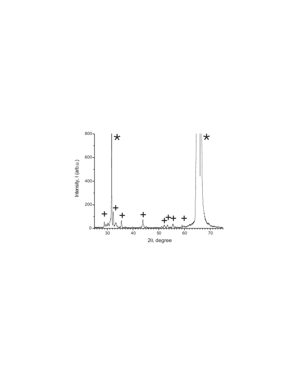
The structure of YIG films was determined by the X-ray diffraction (XRD CuK) method and by the energy-dispersive X-ray spectroscopy. The XRD spectrum confirms the existence of the YIG phase in the sample (Fig. 2). It is found that YIG films are polycrystal and are of homogeneous phase structure. The spectroscopy methods have shown that the interface layer of GaAs is enriched with Ga due to the volatility of As ions, however, the deposited YIG films are not degraded and are not exfoliated from the GaAs substrates.
III Magnetic characteristics of YIG films
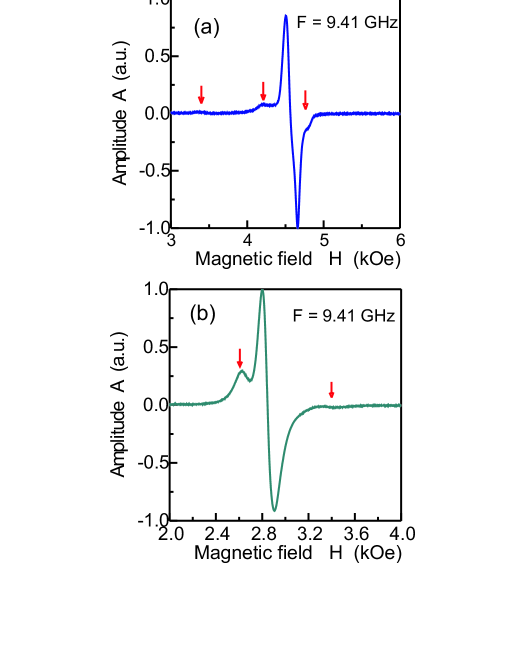
Ferromagnetic resonance of sputtered YIG films was studied by the X-band electron spin resonance technique. Relating to samples, applied magnetic field had in-plane and perpendicular orientations. Using magnetic field sweeping at stabilized frequency GHz, we have read the first derivative of the FMR curve with respect to the magnetic field . FMR spectrum of the YIG film with the thickness of 40 nm (sample # 1, Table 1) at perpendicular and at in-plane magnetic fields are presented in Fig. 3. Arrows correspond to FMR peaks of YIG sublayers.
In order to find magnetic characteristics of the main YIG layer and sublayers, we use the Lorentzian fitting of experimental curves. Experimental curves are fitted by the sum of first derivatives of Lorentzian curves
| (1) |
where is the peak number ( is the number of the main YIG layer and are numbers of sublayers), is the amplitude,
is the Lorentzian curve, is the peak position, is the FMR linewidth. From the Lorentzian fitting (1) we find peak positions and the FMR linewidth .
Differences between magnetization and uniaxial anisotropy field (effective magnetization) of the main YIG layer and YIG sublayers are found from the FMR peak position of the corresponding layer at the in-plane magnetic field Gur96
| (2) |
and from the FMR peak position at the perpendicular field
| (3) |
where 2.83 MHz/Oe is the gyromagnetic ratio. Taking into account Eqs. (2) and (3), values of the effective magnetization of main YIG layers and YIG sublayers are found. Effective magnetizations and FMR linewidthes and of main YIG layers are presented in Table 1. We note that samples # 1, 2, 4 annealed in the air atmosphere have higher values of the effective magnetization and lower values of the FMR linewidth than samples # 3, 5, 6 annealed in the N2 atmosphere. The reason for the YIG sublayer formation is not well clear up to now and it is planned to be clarified in next study.
IV Spin waves
The FMR linewidth measurement is not sufficient for the determination of relaxation of spin excitations. The linewidth is formed by relaxation of spin excitations and by magnetic inhomogeneity of a magnetic film. In order to determine the relaxation parameters, one should study spin wave propagation directly. We studied the amplitude-frequency characteristics and the relaxation of the Damon -Eshbach surface spin waves DE in the in-plane oriented magnetic field. The setup is presented in Fig. 4a. The spin-wave measurement cell contains microstrip antennas. The samples are placed on the antenna structure. Antennas generate and receive spin waves propagated in YIG films. The studied samples are irregular trapezoidal with sizes of mm. The distance between antennas in the cell was set to 1.2 mm. The thickness of antennas is of 30 m. The excited spin-wave wavelength is given by the thickness and is in the range . The antenna length is equal to 2 mm. The measurement setup contains the Rohde-Schwarz vector network analyzer ZVA-40, which generates the current flowing in the generating antenna and detects the current induced by spin waves in the receiving one. We measure amplitude-frequency characteristics which are the transmission coefficient (the scalar gain) in the frequency range of 3.0–4.8 GHz and in the applied magnetic field 862 Oe with the in-plane orientation. Only for the sample # 4 we could detect the transmission coefficient (Fig. 4b). For other samples, the spin-wave relaxation appeared to be much faster and we could not detect the spin-wave signals on the receiving antenna.
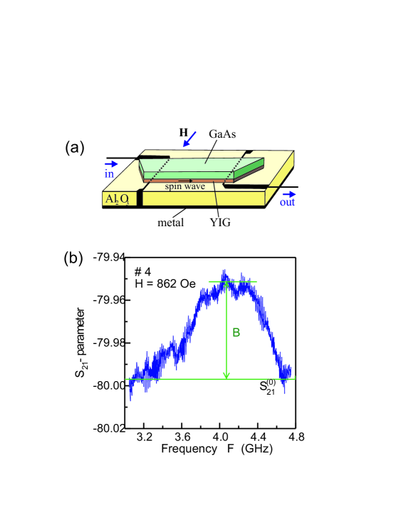
Measuring the -parameter, we can estimate the lower bound of the spin-wave relaxation time () Stog15a ; Lut16 . For this estimation we take into account the following approximations.
(1) We suppose that .
(2) In order to calculate spin-wave velocity, we substitute YIG films with inhomogeneity through thickness by homogeneous films with higher velocity of propagating spin waves.
(3) The energy transformations current spin waves and spin waves current in antenna structure are perfect and have not losses.
The -parameter with the voltage induced by spin waves on the receiving antenna and without spin waves can be written, respectively, as
| (4) |
where is the voltage induced by spin waves on the receiving antenna in the magnetic field 862 Oe, is the voltage on the receiving antenna without a magnetic field and, consequently, without spin waves, is the voltage on the generating antenna. We suppose that the spin-wave signals and the voltage are not correlated. The voltage induced by spin waves is reduced according to
| (5) |
where is the group velocity of spin waves, is the distance between antennas. The spin-wave velocity is given by Stan09 ; Kabos ; Gur96 ; DE
| (6) |
where is the frequency at the spin wave dispersion curve at which the wavevector , is the thickness of the YIG film. Solving the equations (4), (5), and (6), we find that the spin-wave relaxation time s and the spin-wave damping parameter, which is given by Gur96 ; Sparks64
| (7) |
is equal to . In relation (7) and . Taking into account this value of the spin-wave damping parameter, we can find the contribution of the relaxation process to the FMR linewidth, which is about 2 % of the linewidth . Thus, we can suppose that the main contribution to the FMR linewidth of the sputtered YIG film is due to a magnetic inhomogeneity through the film thickness. The analogous magnetic inhomogeneity has been observed in YIG films sputtered on GaN substrates Stog15a . The detailed analysis of the evaluation of the spin-wave damping parameter in inhomogeneous YIG films is presented in Ref. Stog15a .
V Influence of spin excitations on the 2DEG current
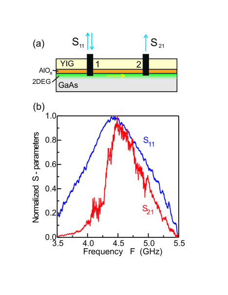
Two-dimensional electron gases are formed at oxide interfaces Koo05 ; Mann08 . In order to study interaction between spin excitations in the YIG film and 2DEG in GaAs at the AlOx / GaAs interface, we have performed the transistor structure with 2DEG channel on the samples # 3 and # 6. Electrical contacts are formed by using the silver paste. We measure amplitude–frequency characteristics which are the transmission coefficient and the voltage reflection coefficient in frequency range of 3.5–5.5 GHz and in applied magnetic fields up to 6 kOe with the in-plane orientation. The -parameter matrix for the 2-port network is defined as , where is the voltage wave reflected from the -contact and is the incident wave at the -contact Choma07 . The electrical resistivity of YIG films is considerably higher than the resistivity of the GaAs substrate ( cm), consequently, the channel conductivity between contacts is due to the GaAs 2DEG interface region (Fig. 5a). In the FMR frequency band the YIG-film spin excitations give an influence on the current flowing through the GaAs channel. The measurement setup contains the Rohde-Schwarz vector network analyzer ZVA-40, which generates the current flowing through the 2DEG channel and detects reflected () and passed () signals. Normalized -parameters measured in sample # 3 in the magnetic field 1.107 kOe at the microwave power 10 dBm are shown in Fig. 5b. One can see that the linewidth of the transmission coefficient (593 MHz) is less than the linewidth of the reflection coefficient (1215 MHz). This difference can be explained by a magnetic inhomogeneity of the YIG film over the thickness . The -parameter is formed by the inner volume, upper and YIG / AlOx interface regions of the YIG film near the first contact. On the contrary, the -parameter is formed by the 2DEG channel and the neighboring YIG / AlOx interface region. In comparison with inner volume and upper regions, the neighboring interface region of the YIG film give the greater contribution to the -parameter. Since magnetic parameters of the inner volume, upper and interface YIG regions can be different, this leads to the difference between and parameters. The observed interaction between spin excitations and 2D electrons is of the electromagnetic nature. The alternating magnetic field of spin excitations induces an alternating electrical field, which influences on 2D electrons. The observed influence of spin excitations on the 2DEG current results in modulation of the current flowing in the 2DEG channel and, in this sense, one can say that this modulation is analogous to the action of a gate electrical potential in FET-structures.
VI Inverse effect. Influence of the current on spin excitations
In order to observe the inverse effect – influence of the current on spin excitations and to enhance this inverse effect, we have carried out the experiment under the following conditions: (1) high channel conductivity, (2) low values of the microwave frequency, at which the three-magnon decay occurs, and (3) high values of the microwave power. Increase of the 2DEG current caused by the growth of the channel conductivity leads to the increase of an alternating magnetic field acted on the YIG film and at high microwave powers results in essential changes in the FMR spectrum. According to Gur96 , at the three-magnon decay of the FMR excitation at high microwave powers this influence can be rather high. In the in-plane magnetic field spin excitations can decay into backward volume spin waves.
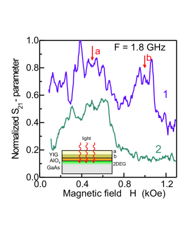
In order to increase the channel conductivity in the transistor structure formed on the sample # 6, the channel was exposed by a light beam ( = 650 nm, = 1.907 eV) with the photon energy greater than the GaAs energy band gap of 1.424 eV and less than the YIG band gap of 2.85 eV Lars75 and the AlOx band gap of 6.5 eV Nigo12 . The light beam was linearly polarized with the intensity mW/cm2. The light exposure leads to electron density increase in the GaAs 2DEG channel and it is analogous to an action of electric field in FET structures. Resistance of the channel is reduced from 28.0 M to 16.9 M. As a result of the light exposure, the local microwave intensity at neighbouring YIG / AlOx interface region increases. This leads to the three-magnon decay of the FMR excitation in the YIG interface layer. The magnon instability process appears at the frequency 1.8 GHz and at the microwave power 10 dBm. The normalized -parameters measured in the sample # 6 at the frequency 1.8 GHz and at the microwave power 14 dBm under the light exposure and without light are shown in Fig. 6. Dependencies are normalized by the maximum value of the -parameter measured under the light exposure. The increase of electrons in the 2DEG channel induced by light leads to essential changes in the FMR spectrum and in the -parameter. One can see that an additional FMR peak appears in applied magnetic field of 1 kOe. One can observe a decrease in the height of the peak and a growth in the amplitude of the peak , while decreasing frequency of the incident microwave signal and keeping the microwave power constant and equal to 14 dBm. Therefore, one can conclude that this leads to an increase of the thickness of the YIG layer , where the magnon instability process occurs.
VII Conclusion
In summary, we described synthesis of YIG films sputtered on AlOx / GaAs substrates, determined their magnetic characteristics, studied properties of the spin wave propagation and the influence of spin excitations in YIG films and 2DEG channels formed at the AlOx / GaAs interface. It is found that the contribution of the relaxation process to the ferromagnetic resonance (FMR) linewidth is about 2 % of the linewidth . At the same time, for all samples FMR linewidths are high. It is supposed that increasing of the FMR linewidth is due to magnetic inhomogeneity of YIG films. High interaction between spin excitations and the electron current flowing through the 2DEG channel formed at the AlOx / GaAs interface is achieved at the FMR frequency of YIG films. On the other hand, above the spin-wave instability threshold the growth of the channel conductivity induced by the light illumination results in essential changes in the FMR spectrum and in the -parameter of the channel. The interaction between the spin excitations in YIG film and 2DEG channel current is increased with the light exposure of the AlOx / GaAs interface and with microwave power growth. The observed interaction is of great importance for active control and manipulation of spin degrees of freedom in field-effect transistors at microwave frequencies.
Acknowledgments
This work was supported by the Russian Science Foundation (project 17-12-01314) and the Russian Foundation for Basic Research (project 15-02-06208).
e-mail: l_lutsev@mail.ru
References
- (1) Z. Chen and V.G. Harris, J. Appl. Phys. 112, 081101 (2012).
- (2) D.D. Stancil and A. Prabhakar, Spin Waves. Theory and Applications (Springer, New York, 2009).
- (3) P. Kabos and V.S. Stalmachov Magnetostatic Waves and Their Applications (Chapman, New York, 1994).
- (4) M. Mruczkiewicz, E.S. Pavlov, S.L. Vysotsky, M. Krawczyk, Yu.A. Filimonov, and S.A. Nikitov, Phys. Rev. B 90, 174416 (2014).
- (5) V.D. Bessonov, M. Mruczkiewicz, R. Gieniusz, U. Guzowska, A. Maziewski, A.I. Stognij, and M. Krawczyk, Phys. Rev. B 91, 104421 (2015).
- (6) S.L. Vysotskii, Y.V. Khivintsev, V.K. Sakharov, G.M. Dudko, A.V. Kozhevnikov, S.A. Nikitov, N.N. Novitskii, A.I. Stognij, and Y.A. Filimonov, IEEE Magnetic Letters 8, (2017) 3706104 (2017).
- (7) S.A. Manuilov, R. Fors, S.I. Khartsev, and A.M. Grishin, J. Appl. Phys. 105(3), 033917 (2009).
- (8) A.I. Stognij, L.V. Lutsev, V.E. Bursian, and N.N. Novitskii, J. Appl. Phys. 118, 023905 (2015).
- (9) A. Stognij, L. Lutsev, N. Novitskii, A. Bespalov, O. Golikova, V. Ketsko, R. Gieniusz, and A. Maziewski, J. Phys. D: Appl. Phys. 48, 485002 (2015).
- (10) L.V. Lutsev, A.M. Korovin, V.E. Bursian, S.V. Gastev, V.V. Fedorov, S.M. Suturin, and N.S. Sokolov, Appl. Phys. Lett. 108, 182402 (2016).
- (11) L.V. Lutsev, Phys. Rev. B 85, 214413 (2012).
- (12) S. Datta and B. Das, Appl. Phys. Lett. 56, 665 (1990).
- (13) K. Hall, W.H. Lau, K. Gundogdu, M.E. Flatte, and T.F. Boggess, Appl. Phys. Lett. 83, 2937 (2003).
- (14) J. Schliemann, J.C. Egues, and D. Loss, Phys. Rev. Lett. 90, 146801 (2003).
- (15) J.C. Egues, G. Burkard, and D. Loss, Appl. Phys. Lett. 82, 2658 (2003).
- (16) I. Žutic, J. Fabian, and S. Das Sarma, Rev. Mod. Phys. 76, 323 (2004).
- (17) S. Sugahara, Phys. Stat. Sol. 12, 4405 (2006).
- (18) X. Lou, Ch. Adelmann, S.A. Crooker, E.S. Garlid, J. Zhang, K.S.M. Reddy, S.D. Flexner, Ch.J. Palmstrøm, and P.A. Crowell, Nature Physics 3, 197 (2007).
- (19) H.C. Koo, J.H. Kwon, J. Eom, J. Chang, S.H. Han, and M. Johnson, Science 325, 1515 (2009).
- (20) P. Chuang, S.-C. Ho, L.W. Smith, F. Sfigakis, M. Pepper, C.-H. Chen, J.-C. Fan, J.P. Griffiths, I. Farrer, H.E. Beere, G.A.C. Jones, D.A. Ritchie, and T.-M. Chen, Nature Nanotechnology 10, 35 (2015).
- (21) H. Buhay, J.D. Adam, M.R. Daniel, N.J. Doyle, M.C. Driver, G.W. Eldridge, M.H. Hanes, R.L. Messham, and M.M. Sopira, IEEE Trans. Magn. 31, 3832 (1995).
- (22) Solid State Physics. Recent Advances in Magnetic Insulators – From Spintronics to Microwave Applications, Edd. M. Wu and A. Hoffmann (Academic Press, San Diego, 2013).
- (23) G.D. Nipan, A.I. Stognij, and V.A. Ketsko, Russian Chemical Reviews 81, 458 (2012).
- (24) A.I. Stognij, V.V. Tokarev, and Yu.N. Mitin, Mat. Res. Soc. Symp. Proc. 236, 331 (1992).
- (25) H.C. Koo, H. Yi, J.B. Ko, J.D. Song, J. Chang, and S.H. Han, J. Magnetics 10, 66 (2005).
- (26) J. Mannhart, D.H.A. Blank, H.Y. Hwang, A.J. Millis, and J.-M. Triscone, MRS Bulletin 33, 1027 (2008).
- (27) A.G. Gurevich and G.A. Melkov, Magnetization Oscillations and Waves (CRC Press, New York, 1996).
- (28) R.W. Damon and J.R. Eshbach, J. Phys. Chem. Solids 19, 308 (1961).
- (29) M. Sparks, Ferromagnetic-Relaxation Theory (McGraw-Hill, New York, 1964).
- (30) J. Choma and W.K. Chen, Feedback Networks: Theory and Circuit Applications (World Scientific, Singapore, 2007).
- (31) P.K. Larsen and R. Metselaar, J. Solid State Chemistry 12, 253 (1975).
- (32) S. Nigo, M. Kubota, Y. Harada, T. Hirayama, S. Kato, H. Kitazawa, and G. Kido, J. Appl. Phys. 112, 033711 (2012).