On the charge and magnetic ordering in monolayer NbSe2:
a first principles study
Abstract
Monolayer NbSe2 has recently been shown to be a 2-dimensional superconductor, with a competing charge-density wave (CDW) order. This work investigates the electronic structure of monolayer NbSe2 based on first principles calculations, focusing on charge and magnetic orders in connection to the superconductivity. It is found that decreased screening in the monolayer NbSe2 with a perfect lattice exhibits magnetic instability, which is removed by the formation of CDW. Two energetically competitive but distinct CDW structures are revealed computationally, which have a significant impact on the Fermi surface. The relations of the potential CDW phases with experimental structure and the coexisting superconductivity are discussed.
Layered transition metal dichalcogenides (TMDCs) MX2, where M is a transition metal and X is a chalcogen, are a remarkable class of materials displaying a multitude of correlation effects, ranging from CDW, magnetic ordering to superconductivity. In recent years, TMDCs have become available in monolayer forms Xi2015 ; Sarkar2015 ; Wang2012 ; Tang2017 ; Li2015 . In particular, monolayer niobium diselenide, NbSe2, has an extraordinarily rich phase diagram with respect to temperature. In the bulk form, NbSe2 is one of the first materials found to host coexisting CDW and superconducting orders Revolinsky1965 ; Moncton1975 . In the monolayer limit, superconductivity again coexists with the CDW order, with a superconducting = 1.9 K Ugeda2015 compared with the bulk value 7 K. A commensurate charge-density wave (CDW) transition was found at 145 K Xi2015 , with CDW vector , corresponding to a structural reconstruction within a 33 supercell. In the monolayer limit, on the other hand, it is well known that screening is significantly reduced compared to the bulk counterpart, leading sometimes to dramatically enhanced electronic correlation. Indeed, previous first principles calculations suggest possible antiferromagnetic order in monolayer NbSe2 in the absence of CDW order Xu2014 ; Zhou2012 . The above observations indicate that the correlations arising from lattice and interaction are both important in monolayer NbSe2.
On account of such multi-correlated nature, the interplay of different correlation effects, and therefore possible phases of monolayer NbSe2, are yet to be clarified, which requires treating different instabilities on the same footing. One aim of the present paper, therefore, is to analyze the equilibrium atom arrangement in the CDW phase of monolayer NbSe2, and at the same time, the competition between the CDW and magnetic instabilities. It is revealed that the formation of CDW phase eventually suppresses the magnetic instability, providing clarification to the vagary regarding the absence of magnetic order in monolayer NbSe2. A second objective of this paper is to understand the electronic structure of monolayer NbSe2, in the eventual low-temperature CDW phase. A Brillouin zone unfolding scheme is devised to compare the Fermi surface of the CDW phase to that of the symmetric lattice phase. Whereas the monolayer NbSe2 with symmetric lattice has three Fermi circles, at , and , respectively, the CDW order leaves them partially or fully gapped. The extensive obliteration of the computed Fermi surface leads to an explanation for the disappearance of the magnetic instability, and potentially, for the lower-than-bulk superconducting for monolayer NbSe2.
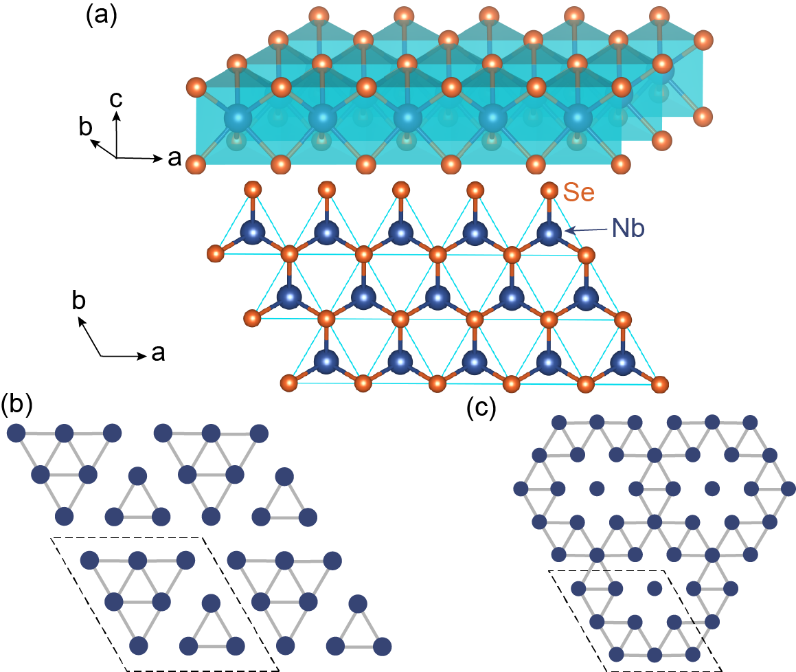
The structure of the monolayer NbSe2 without CDW, isolated from the bulk phase -NbSe2, forms a 2-dimensional hexagonal lattice in the 2-dimensional space group , as shown in Fig. 1(a). It is composed of three layers of atoms, with a Nb layer sandwiched between Se layers. Each Nb atom sits inside a trigonal prismatic cage formed by six nearest-neighbor Se atoms. Nb atoms form a perfect hexagonal closest packing structure, with the shortest Nb-Nb separation Å according to our calculations SM . This non-CDW phase of monolayer NbSe2 is found to be unstable below Calandra2009 and exhibits pronounced soft phonon mode around in our calculations, indicating a strong structural instability to the formation of a 33 supercell.
Density-functional theory (DFT) calculations were performed, within the generalized gradient approximation (GGA), parameterized by Perdew, Burke, and Ernzerhof (PBE) to investigate the crystal structure, electronic structure and lattice dynamics of monolayer NbSe2 in non-CDW and CDW phase Kresse1996 ; Perdew1996 . The Kohn-Sham valence states were expanded in the plane wave basis set with a kinetic energy truncation at 530 eV. An 18181 and a 661 -grid centered at point were chosen for the sampling of the Brillouin zones of the non-CDW and CDW phase respectively. The equilibrium crystal structure was determined by a conjugated-gradient relaxation of ionic positions, until the Hellmann-Feynman force on each atom was less than 0.005 Å/eV and a zero-stress tensor was obtained. Crystal structure of the NbSe2 in the CDW state was obtained with multiple structural optimizations with a 33 supercell. Before each optimization, small random displacements were added to each atom to remove all discrete symmetries.
When the structure of monolayer NbSe2 is relaxed in a supercell, the CDW indeed forms, which can be characterized by a reconstruction of the Nb atomic layer, with concomitant displacements of Se atoms. Besides, we also examine the lattice stabilities of the three reconstructed CDW phases under different in-plane lattice constants and using different types of exchange-correlation functionals, which give rise to similar results as described in the supplemental material SM . Using the fully relaxed in-plane lattice constant Å, two CDW reconstructions are found to be important, referred to herein as triangle and star phases (see supplemental material for details SM ). Fig. 1(b) displays the triangle phase, where the Nb atoms are grouped into large and small triangular clusters, consisting of six and three Nb atoms respectively within a 33 supercell. The star phase is characterized by overlapping star-shaped clusters, as displayed in Fig. 1(c), which is similar to bulk -NbSe2 in CDW state Malliakas2013 ; Silva2016 .
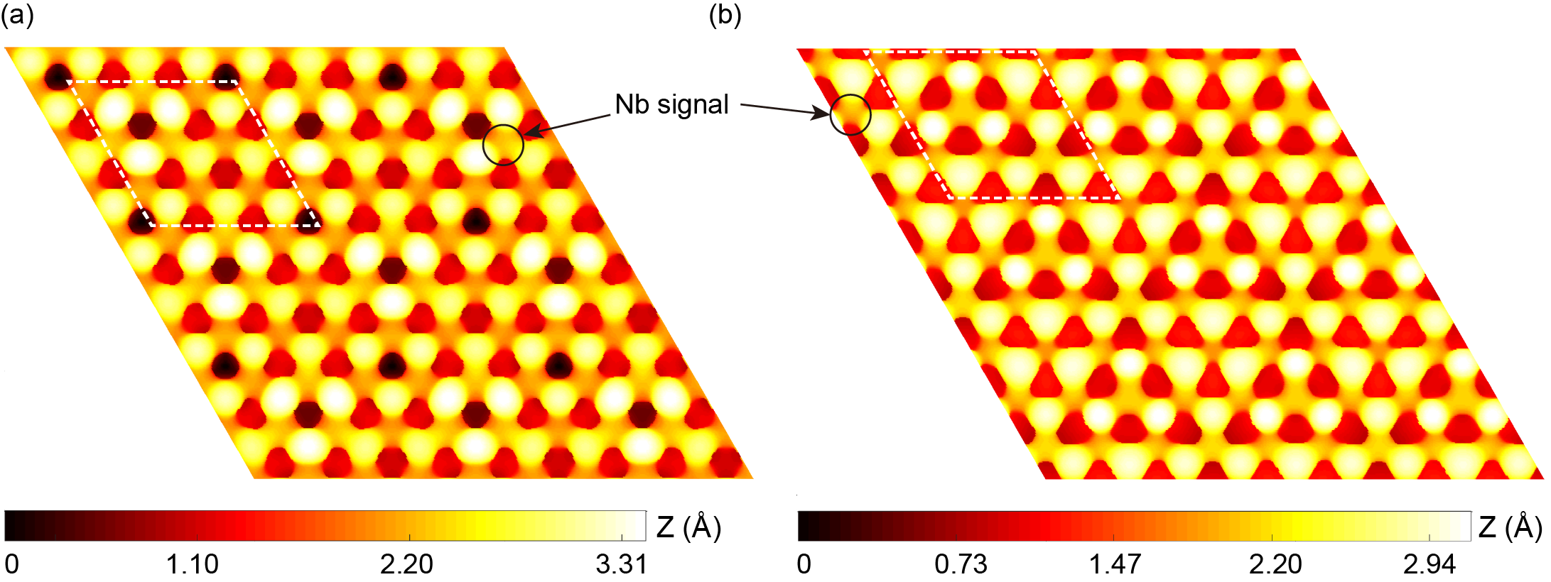
The topography of monolayer NbSe2 in the CDW phase, which may be revealed by scanning-tunneling microscopy (STM), is simulated. We compute the local electronic density of states, averaged over an energy window below the Fermi level
| (1) |
where is the Kohn-Sham wavefunction of the th band at wavevector , the Fermi energy, the width of the energy window, and the area of a supercell. The energy window is set to meV. The simulated STM topography, , is subsequently determined by the implicit equation, , where the iso-density value 6.3 Å2 is used to best match the experimental STM topography Xi2015 . Since the tunneling current is proportional to local density of states, can be interpreted semiquantitively as the topography revealed in a constant-current STM topographical scan.
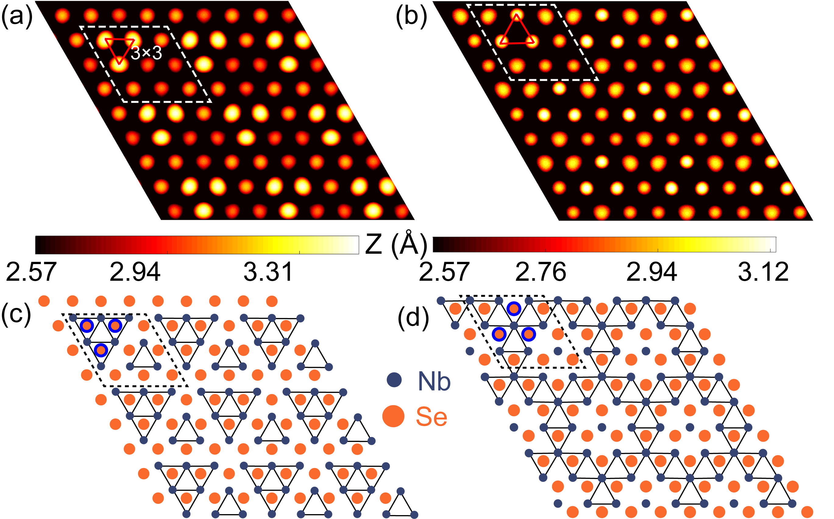
The simulated STM topographies of the triangle and star CDW phases are displayed in Fig. 2. The STM topography is dominated by top Se atoms (see Fig. S2 SM ), despite that the electronic states around the Fermi level arise mostly from the -orbitals of Nb atoms. Furthermore, the dominant STM feature of the triangle phase is contributed by the three Se atoms on the top of the large triangular cluster, shown as a red triangle as displayed in Figs. 2(a) and 2(c) (marked with three blue circles). Similarly, the star phase can be also characterized by similar red triangles as displayed in Fig. 2(b), attributable to the three top-layer Se atoms, indicated by blue circles in Fig. 2(d). Comparing with the experimental STM topography shown in Fig. 1(e) of the reference Ugeda2015 , which shows an array of small triangles, we find that the simulated STM topographies of triangle and star phases are both consistent with the experiment. Owing to the similarity of STM patterns and energies (see supplemental material SM ) of the triangle and star phases, we are unable to suggest which CDW is more likely to occur in the actual monolayer NbSe2.
In the monolayer limit, the screening is substantially reduced compared to bulk material, giving rise to stronger interaction between electrons. It is then expected that monolayer material is more prone to developing magnetic order even with a non-magnetic bulk counterpart. Previous first principles investigations Xu2014 ; Zhou2012 indicate that the most stable state of monolayer NbSe2 without CDW order is antiferromagnetic in a supercell. The issue, however, remains with whether the magnetic order coexists or competes with the CDW order, both of which are known to modify the Fermi surface and consequently the susceptibility. Therefore, in order to quantify the magnetic instability, we analyse the spin susceptibility of monolayer NbSe2, obtained from tight-binding models based upon Wannier functions extracted from the Kohn-Sham band structures Mostofi2014 .
The general form of noninteracting susceptibilities reads Kubo2007 :
| (2) |
where denoting orbital index, is the number of lattice sites, and , is the amplitude of the th band at crystal momentum on the th Wannier orbital, obtained by diagonalizing the tight-binding Hamiltonian. The static one-loop spin susceptibility is given by . In our non-spin-polarized DFT calculations of supercell of monolayer NbSe2, with and without (triangle or star) CDW and in-between, the manifold of 9 bands around the Fermi level are predominantly formed by Nb orbitals, which are well separated from all other bands. Therefore, these bands are used to construct 9-band tight-binding Hamiltonians.
In order to assess how the magnetic instability evolves as the CDW is developing, we calculated the spin susceptibilities of a series structures interpolated between the non-CDW and CDW phases. Here, the atom posititions of an interpolated supercell is given by , where corresponds to the amplitude of CDW distortions, and and are the positions of atoms in state without and with CDW distortions, respectively. Figs. 3(a)-3(b) show the calculated for different in supercells. When , corresponding to non-CDW phase, the spin susceptibility peaks at around and , which indicates magnetic instability, to the formation of a magnetic supercell. This is consistent with a spin-polarized calculation, leading to a magnetic configuration as shown in Fig. 3(c) Xu2014 . It can be clearly seen that with the increase of , the spin susceptibilities generally decrease for both of the triangle and star CDW, suggesting that as the CDW order forms the magnetic order may eventually disappear. However, the spin susceptibilities of star phase are slightly larger than that of the triangle phase, which indicates that their magnetic behaviors may be different when CDW distortions set in.
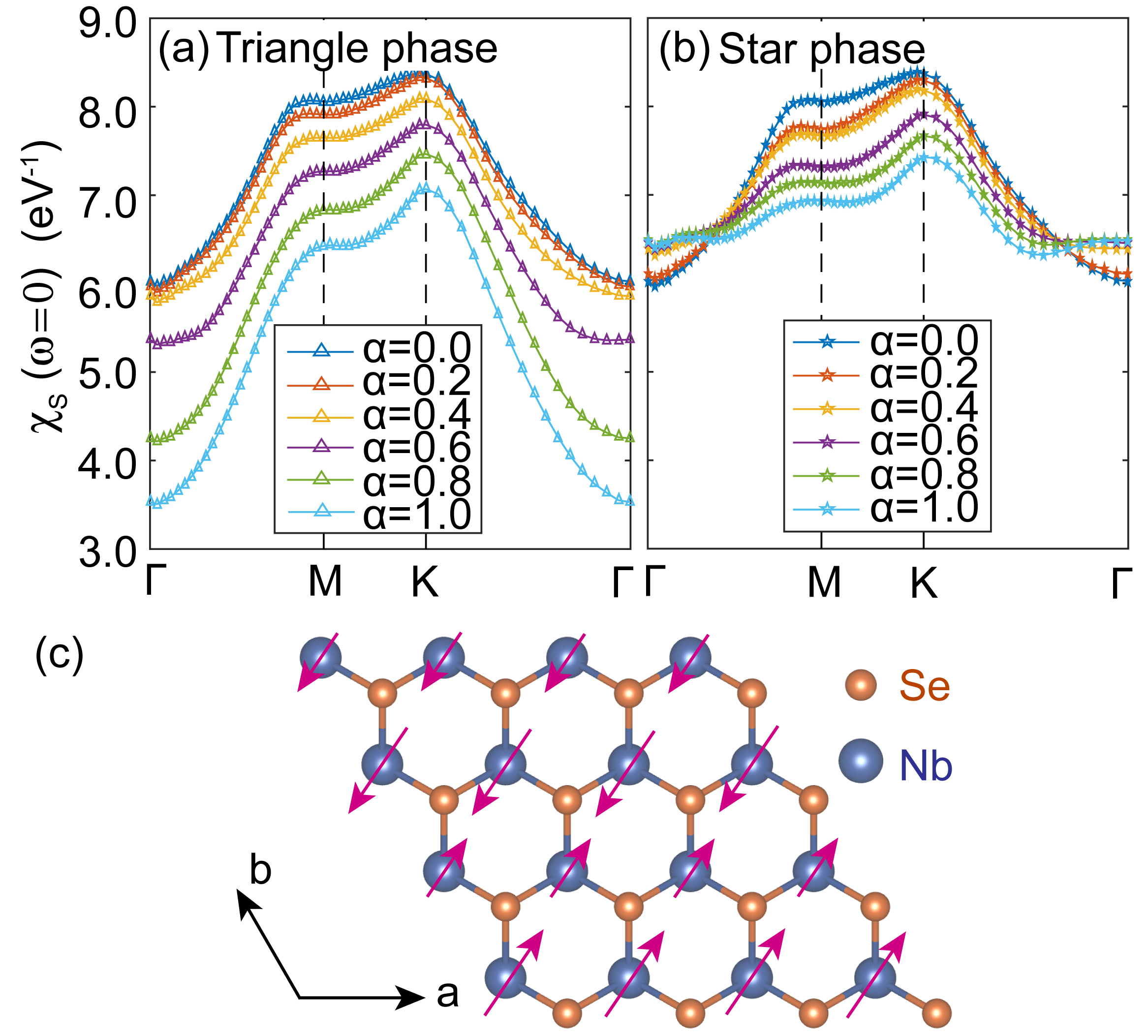
Our spin spiral calculations (see supplemental material for details SM ) suggest that the non-CDW phase of monolayer NbSe2 possesses an antiferromagnetic magnetic ground state as depicted in Fig. 3(c), which is in agreement with previous predictions Xu2014 . According to our spin susceptibility calculations above, this magnetic order may eventually be suppressed or even killed by CDW. As a confirmation, we computed the total energy of a supercell to include in both magnetic and CDW orders. We used the interpolation method described above to get a series structures with different values of and carried out both non-spin-polarized and spin-polarized calculations for each kind of CDW.
Figs. 4(a)-4(b) show the calculated total energies, and Figs. 4(c)-4(d) show the calculated magnetic moments of Nb atoms at various values of for the triangle and star CDW, respectively. It is found that for both kinds of CDW, when an antiferomagnetic order is imposed, the total energy increases with the increase of . Meanwhile, the magnetic moments are suppressed, which indicates a competition between CDW and SDW (spin-density wave). However, things are slightly different for triangle and star CDW. For triangle CDW, it is found that when , magnetic phase, which has a collinear magnetic order as shown in Fig. 3(c), has lower energy than the non-magnetic phase as displayed in Fig. 4(a). As increases, the difference of total energy between magnetic and non-magnetic calculations decreases gradually. At about , the energetic advantage of magnetic phase disappears, beyond which the CDW order suppresses the magnetic order completely, which can be verified from the zero magnetic moments when , as shown in Fig. 4(c).
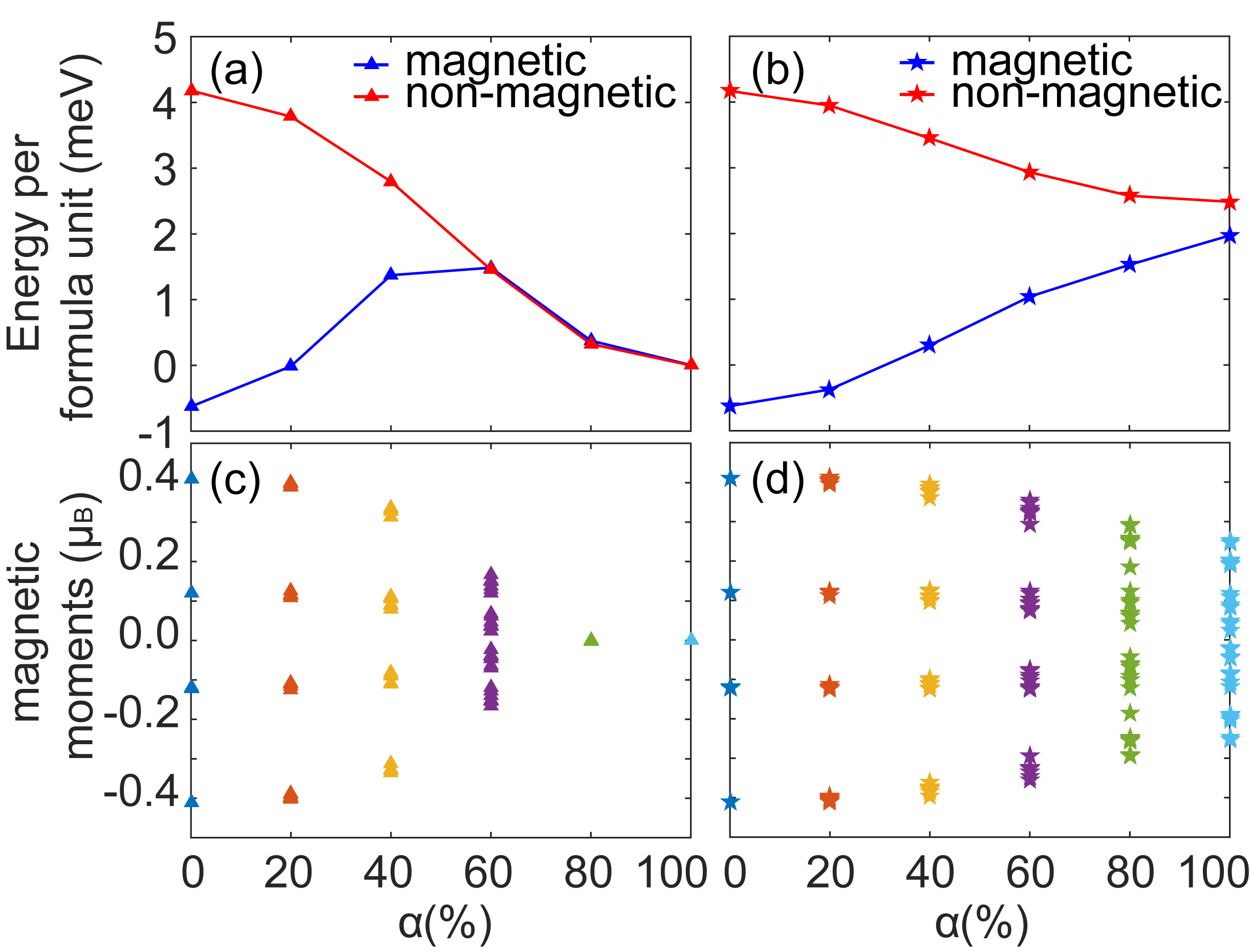
For star CDW, although as increases, the difference of total energies between magnetic and non-magnetic calculations decreases gradually, the magnetic order remains, as shown in Figs. 4(b) and 4(d). The general trend of the magnetic phases’ energies in the two kinds of CDW is also consistent with our previous spin susceptibilities calculations. Base on the results above, we then conclude that without CDW, monolayer NbSe2 favors antiferromagnetic order in a supercell. When the CDW order sets in, the magnetic order is suppressed by the triangle CDW whereas the star CDW may coexist with magnetism.
To investigate the influence of CDW on electronic structure of monolayer NbSe2, band structures and Fermi surfaces of the non-CDW and CDW phases were computed using a 33 supercell and unfolded to the (larger) primitive Brillouin zone of the non-CDW NbSe2, by a weight factor measuring the tranformation of wavefunctions under primitive lattice translations (see supplemental material for details SM ).
As shown in Fig. 5(a), the Fermi surface of the non-CDW phase consists of three inequivalent circles (white lines), centered at , and points, respectively. After CDW transition, they are partially or fully gapped due to the lattice distortion. Fig. 5 displays the unfolded Fermi surfaces of the non-CDW phase (a), triangle CDW phase (b), and star CDW phase (c), respectively. It is evident that the triangle phase develops more extensive gapping on the Fermi surface compared to the star phase. Both of the triangle and star CDW phases show significant partial gapping along the Fermi surface encircling , which appears to be more extensive for the triangle phase. Remarkably, while the -, -centered Fermi circles are only partially gapped in the star phase, they are almost completely obliterated in the triangle phase. The computed electronic density of states also show the consistent results. As displayed in Fig. 5(d), the density of states of star phase at the Fermi level exhibits slight decrease, compared with that of the non-CDW phase. In contrast, the triangle phase shows a more pronounced reduction of the Fermi density of states, corresponding to the more extensive CDW gap on the Fermi surface.
The modification of the Fermi surface also provides a microscopic insight into the interplay between CDW, SDW and superconductivity. In the non-CDW phase with the intact Fermi surface, there exist electronic instabilities which can potentially trigger CDW or SDW. In the presence of the CDW along with the modification of Fermi surface, the SDW instability was subdued as discussed above. It suggests that the electronic states triggering SDW are also responsible for the CDW instability, which are removed from Fermi surface when the CDW forms.
In summary, our calculations reveal that the formation of CDW in monolayer NbSe2 suppresses the magnetic instability of the initiating lattice. Two possible CDW phases are identified computationally, which have similar STM topographical features in our simulation. The formation of CDW gap on the Fermi surface, as visualized from our band unfolding scheme, should also have an important impact on superconductivity. It is expected that the extent of CDW gap is inversely related to the superconducting . The Fermi gapping is substantially more extensive in the triangle phase, in comparison with the bulk-like star phase. In view of the substantially lower of the monolayer NbSe2 compared to the bulk and our computational observation that the star CDW phase remains magnetic, these results potentially favor the hypothesis that the triangle CDW might actually form.
Acknowledgements.
This work was supported by National Natural Science Foundation of China (Grant No. 11725415), and Ministry of Science and Technology of the People’s Republic of China (Grant No. 2016YFA0301004). Part of the calculations were performed on the Tianhe-I Supercomputer System.References
- (1) X. Xi, L. Zhao, Z. Wang, H. Berger, L. Forró, J. Shan, and K. F. Mak, Nat. Nanotechnol. 10, 765 (2015).
- (2) D. Sarkar, X. Xie, W. Liu, W. Cao, J. Kang, Y. Gong, S. Kraemer, P. M. Ajayan, and K. Banerjee, Nature 526, 91 (2015).
- (3) Q. H. Wang, K. Kalantar-Zadeh, A. Kis, J. N. Coleman, and M. S. Strano, Nat. Nanotechnol. 7, 699 (2012).
- (4) S. Tang, C. Zhang, D. Wong, Z. Pedramrazi, H.-Z. Tsai, C. Jia, B. Moritz, M. Claassen, H. Ryu, S. Kahn, et al., Nat. Phys. 13, 683 (2017).
- (5) M.-Y. Li, Y. Shi, C.-C. Cheng, L.-S. Lu, Y.-C. Lin, H.-L. Tang, M.-L. Tsai, C.-W. Chu, K.-H. Wei, J.-H. He, et al., Science 349, 524 (2015).
- (6) E. Revolinsky, G. Spiering, and D. Beerntsen, J. Phys. Chem. Solids 26, 1029 (1965).
- (7) D. Moncton, J. Axe, and F. DiSalvo, Phys. Rev. Let. 34, 734 (1975).
- (8) M. M. Ugeda, A. J. Bradley, Y. Zhang, S. Onishi, Y. Chen, W. Ruan, C. Ojeda-Aristizabal, H. Ryu, M. T. Edmonds, H.-Z. Tsai, A. Riss, S.-K. Mo, D. Lee, A. Zettl, Z. Hussain, Z.-X. Shen, and M. F. Crommie, Nat. Phys. 12, 92 (2015).
- (9) Y. Xu, X. Liu, and W. Guo, Nanoscale 6, 12929 (2014).
- (10) Y. Zhou, Z. Wang, P. Yang, X. Zu, L. Yang, X. Sun, and F. Gao, ACS Nano 6, 9727 (2012).
- (11) Supplemental material.
- (12) M. Calandra, I. I. Mazin, and F. Mauri, Phys. Rev. B 80, 241108 (2009).
- (13) G. Kresse and J. Furthmüller, Phys. Rev. B 54, 11169 (1996).
- (14) J. P. Perdew, K. Burke, and M. Ernzerhof, Phys. Rev. Lett. 77, 3865 (1996).
- (15) C. D. Malliakas and M. G. Kanatzidis, J. Am. Chem. Soc. 135, 1719 (2013).
- (16) J. Á. Silva-Guillén, P. Ordejón, F. Guinea, and E. Canadell, 2D Mater. 3, 35028 (2016).
- (17) A. A. Mostofi, J. R. Yates, G. Pizzi, Y.-S. Lee, I. Souza, D. Vanderbilt, and N. Marzari, Comput. Phys. Commun. 185, 2309 (2014).
- (18) K. Kubo, Phys. Rev. B 75, 224509 (2007).
SUPPLEMENTAL MATERIALS
S1 Geometry structures of the CDW phases and their lattice stabilities
This part mainly reports the details of the geometry structures and lattice stabilities of the triangle, triangle* and star CDW phases obtained at Å as supplemental information of the main text. Three types of reconstructed structures were obtained. Two of the structures are characterized by triangular clusters (the triangle and triangle* phase). Fig. S6(a) displays the triangle phase, where the Nb atoms are grouped into large and small triangular clusters, consisting of six and three Nb atoms respectively within a 33 supercell. The shorten Nb-Nb pairs after CDW transition can be classified as three types according to their distances marked by gray bonds with different thicknesses as illustrated in Fig. S6(a) and the corresponding distances were listed in Table S1. This structure exbihits the lowest total energy.
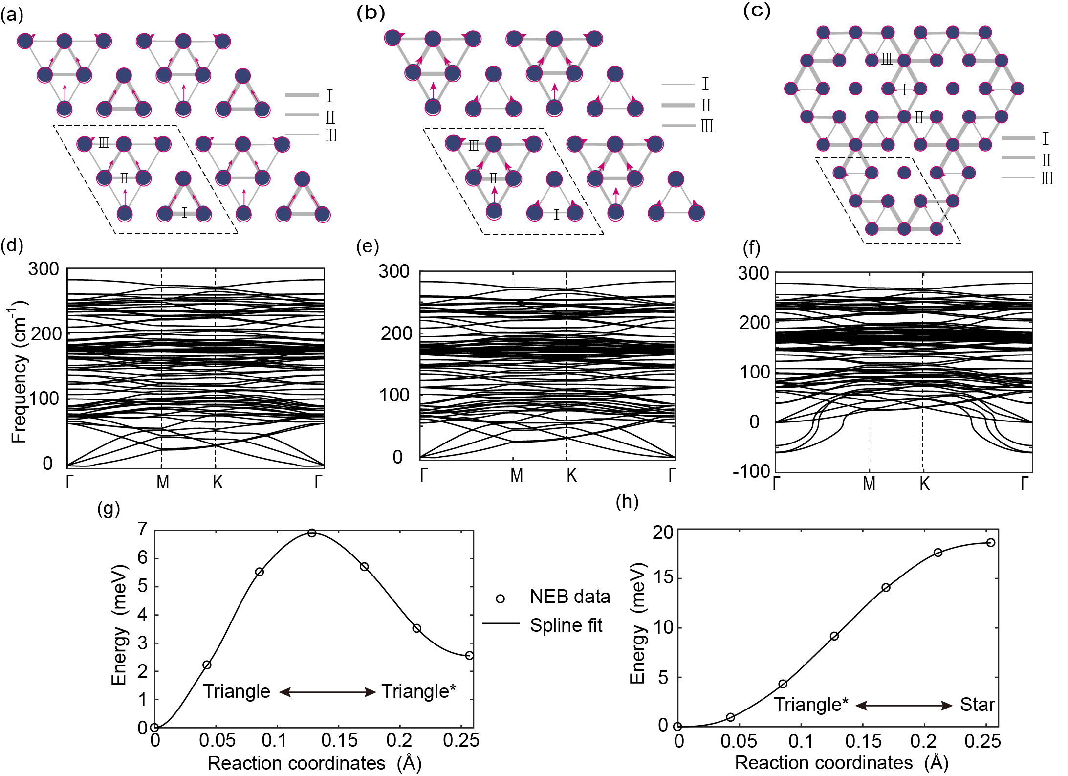
The distributions of Nb atoms between the phases of triangle and triangle* are very similar as shown in Figs. S6(a)-S6(b). The only difference lies in the distance of the bond I as listed in Table S1. In detail, among the shorten pairs of Nb-Nb, the bond I are the shortest in triangle phase but the largest in triangle* phase, which exhibits a slightly higher total energy as listed in Table S1. Interestingly, both of the two phases are likely to be local minimums of the potential energy surface according to the simulated results of lattice dynamics [Figs. S6(d)-S6(e)] and nudged elastic band (NEB) Jonsson1998 ; Kresse1996 [Fig. S6(g)]. As a further confirmation, phonon spectrum was computed Togo2015 ; Kresse1995 ; Alfe2001 to ensure the obtained structures are free of soft phonon modes. In detail, as shown in Figs. S6(d)-S6(e), the soft mode presenting in the non-CDW phase is completely removed in both triangle and triangle* phases. Furthermore, the transition energy barrier between the two phases was computed. As displayed in Fig. S6(g), the energy barrier is only 7 meV, indicating that the structural transition inbetween is rather easy.
Another reconstructed structure, star phase, was displayed in Fig. S6(c). The star-shape clusters are grouped into two alternative units bounded by I type of Nb-Nb as shown in Fig. S6(c). The Nb layer can be viewed as composed of two sublattices owing to the modulation on Nb-Nb nearest-neighbour bonds. A continuous net of Nb forms a honeycomb lattice, with each of the bipartite sites decorated by a hexagonal cluster. The other sublattice is composed of an isolated Nb. It is easy to find that the displacements of Nb atoms in star phase are much smaller than that in the triangle phase by comparing the lengths of the magenta arrows in Fig. S6(c) with Figs. S6(a)-S6(b). In contrast to the triangle and triangle* phases, the star phase is likely to be a metastable structure as shown in Figs. S6(f) and S6(h).
| Configuration | Nb-Nb I (Å) | Nb-Nb II (Å) | Nb-Nb III (Å) | E (meV/ C.F.) |
|---|---|---|---|---|
| Triangle | 3.33 | 3.37 | 3.41 | 0 |
| Triangle* | 3.42 | 3.38 | 3.40 | 0.3 |
| Star | 3.36 | 3.43 | 3.46 | 2.4 |
| Non-CDW | 3.47 | 3.47 | 3.47 | 3.7 |
| Lattice constant (Å) | Functional | Phase | E (meV/ C.F.) |
|---|---|---|---|
| 3.47a | PBE | Triangle | 0 |
| Triangle* | 0.3 | ||
| Star | 2.4 | ||
| Non-CDW | 3.7 | ||
| 3.399a | LDA | Triangle | 0.7 |
| Triangle* | 0 | ||
| Star | 2.9 | ||
| Non-CDW | 3.3 | ||
| 3.458a | PBE | Triangle | 0 |
| Triangle* | 0.1 | ||
| Star | 2.4 | ||
| Non-CDW | 3.5 | ||
| LDA | Triangle | 0.05 | |
| Triangle* | 0 | ||
| Star | 1.8 | ||
| Non-CDW | 3.4 |
-
a
The lattice constants 3.399 and 3.474 Å are obtained by fully relaxation of the lattices using LDA and PBE respectively. 3.458 Å is the lattice constant of bulk -NbSe2 Malliakas2013 .
We carefully examine the lattice stabilities of the triangle, triangle* and star CDW phases under the in-plane lattice constants of 3.399, 3.474 and 3.458 Å using different types of exchange-correlation functional including LDA, PBE. The values 3.399 and 3.474 Å are the fully relaxed lattice constants using LDA and PBE, respectively. The value 3.458 is the in-plane lattice constant of bulk -NbSe2 reported in the reference Malliakas2013 . The related total energies are listed in Table S2. It is found that all the three CDW phases exist regardless of the lattice constants and exchangle-correlation functional being used. Furthermore, it is reasonable that the total energies of the three CDW phases are found to be lower than that of the non-CDW phase. In detail, the triangle and triangle* phase exhibit similar total energies, which are slightly lower than that of the star phase. In particular, the related total energies of the triangle, triangle* and star phase are 0, 0.3 and 2.4 meV per chemical formula respectively at the lattice constant Å.
S2 The STM topography
In the calculations of the STM topographies for the CDW phases, non-self-consistent calculations was carried out with a denser -grid 4848 after self-consistent calculations. Fig. S7 displays the computed STM topography of monolayer NbSe2 in the triangle and star CDW phases. They are similar to the STM topography displayed in Figs. 2(a) and 2(b) in the main text but with different colorbars. By comparing the STM signals within the 33 CDW supercell (bounded by white dashed lines) in Figs. S7(a) and S7(b) to the atomic positions within the corresponding supercells (bounded by black dashed lines) in Figs. 2(c) and 2(d) in the main text, one can find that the STM signal is dominated by Se atoms.
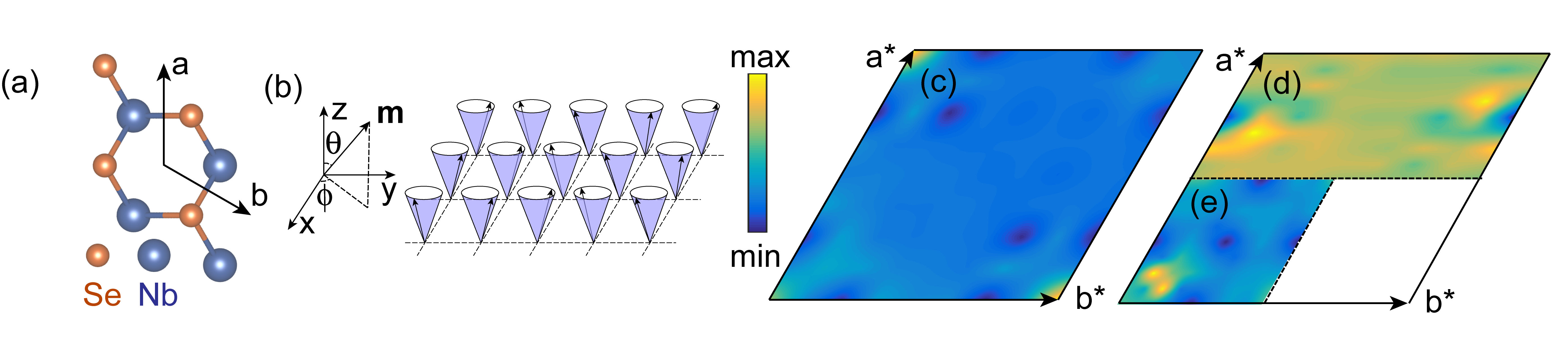
S3 Details of spin spiral calculations
In order to examine the magnetic ground state(s) suggested by the spin susceptibility calculations, spin spiral calculations were carried out to determine the magnetic order of monolayer NbSe2 in non-CDW phase. As depicted in Fig. S8(b), we shall restrict ourselves to a consideration of spin spiral structures of the form Sandratskii1991
| (3a) | |||
| (3b) | |||
| (3c) | |||
| (3d) | |||
where denote the three components of atomic magnetic moments, the are the lattice translations, the are position vectors of atoms within the unit-cell, the is the magnetic moment of the th atom, and is the vector of the spiral order. Although crystal with spin spiral magnetic order loses its translation symmetry, a generalized Bloch theorem allows us to compute the energy of a supercell with spiral magnetic order using and at the computational cost of a primitive cell. This allows us to quickly and accurately survey the energies for different ’s.
As shown in Fig. S8(c), the calculated total energy reaches minima at a* (and other equivalent vectors, a* and b* are reciprocal lattice vectors of primitive cell), indicating a possible magnetic ground state in a supercell. Subsequently, the spiral magnetic order is imposed on and supercells, which allows spin modulation within a supercell. Fig. S8(d) shows the total energy with respect to spiral vectors in supercell, the minima appear at a* (the reciprocal lattice vector in a direction of supercell is half of the primitive cell). The results for supercell are shown in Fig. S8(e), the spiral vectors for the lowest total energy are a* as well. Base on the results of our spin spiral calculations, we infer that a magnetic ground state may appear in a supercell, which are consistent with the magnetic instability indicated by our previours spin susceptibiity calculations. We then did a magnetic calculation in a supercell to finally determine the magnetic order. Fig. 3(c) in the main text shows our calculated antiferromagnetic spin configurations, which is the most stable state in the non-CDW phase, in agreement with previous predictions Xu2014 .
S4 Unfolding electronic structures
In the unfolding calculations for the non-CDW and CDW phases of monolayer NbSe2, 33 CDW supercells are adapted, each containing 27 atoms in total. The Fermi surfaces are computed on a 9696 -grid and subsequently unfolded to the primitive Brillouin zone (PBZ) of the non-CDW phase using unfolding technique Allen2013 . In light of this method, the electronic bands in supercell Brillouin zone are unfolded to PBZ with a weight function which measures the degree of the Bloch symmetry belonging to a primitive cell, that an eignstate of a supercell posesses. The supercell contains primitive cells. donates an eigenstate of the supercell with a band index and a wavevector . is a reciprocal lattice vector of the supercell, connecting to a wavevector in the PBZ as . is the translation corresponding to the th primitive cell in the supercell.
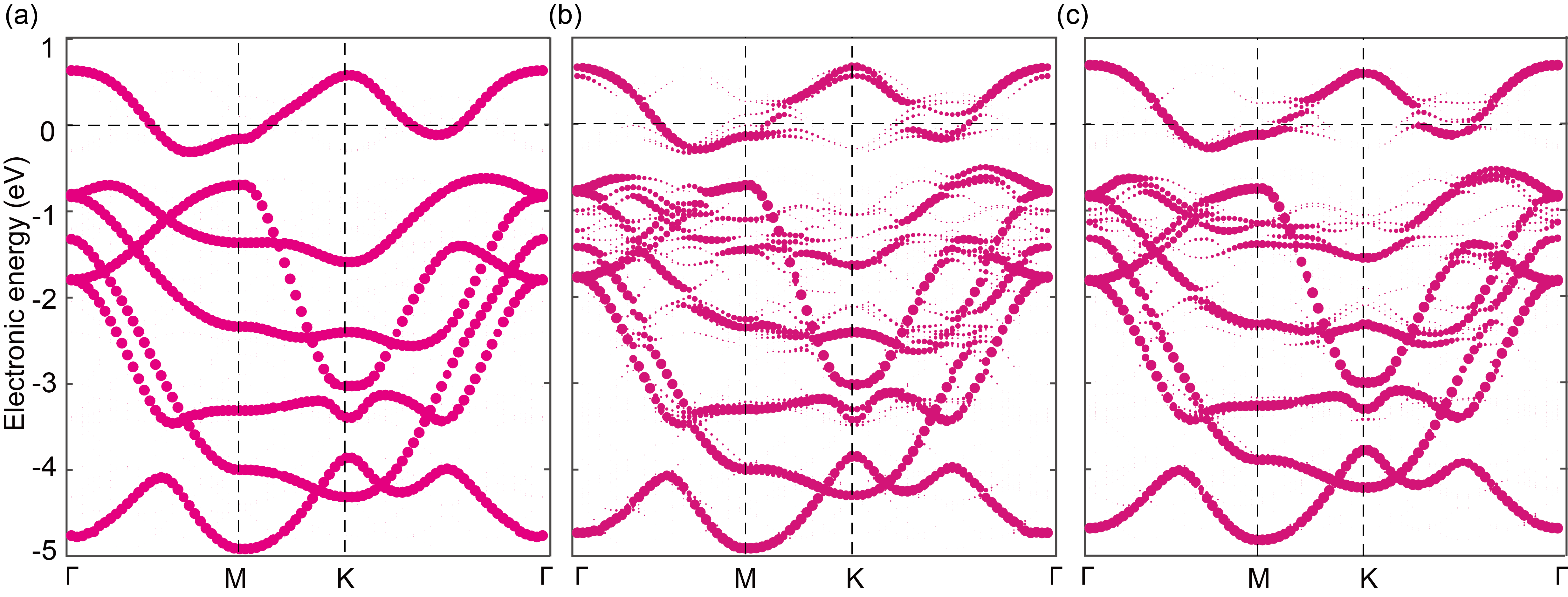
Fig. S9 displays the electronic band structures of non-CDW phase (a), the triangle CDW phase (b), and the star CDW phase (c) of monolayer NbSe2, respectively. The unfolded band structure of the non-CDW phase agrees perfectly with the one directly computed with a primitive cell. The sizes of the red dots are uniform and the corresponding unfolding weights 1. The most prominent changes of the electronic states after the CDW transition are located in the following three regions: -2 -2.5 eV, -0.8 -1.6 eV and around the Fermi level. Some parts of the electronic states are removed compared to that of the non-CDW phase, especially near the momenta at 2/3, 1/3, 1/3 and 2/3. Despite the above changes, the band structures of the CDW phases coincide with that of the non-CDW phase approximatively, indicating that the shapes of the bandsturcutres remain virtually unchanged and there exist negligible energy shifts for each band in the presence of CDW.
References
- (1) G. Kresse and J. Furthmüller, Phys. Rev. B 54, 11169 (1996).
- (2) C. D. Malliakas and M. G. Kanatzidis, J. Am. Chem. Soc. 135, 1719 (2013).
- (3) H. Jónsson, G. Mills, and K. W. Jacobsen, in Classical and Quantum Dynamics in Condensed Phase Simulations, edited by B. J. Berne et al. (World Scientific, Singapore, 1998).
- (4) A. Togo and I. Tanaka, Scr. Mater. 108, 1 (2015).
- (5) G. Kresse, J. Furthmüller, and J. Hafner, Europhys. Lett. 32, 729 (1995).
- (6) D. Alfè, G. D. Price, and M. J. Gillan, Phys. Rev. B 64, 45123 (2001).
- (7) M. Born and R. Oppenheimer, Ann. Phys. 389, 457 (1927).
- (8) L. M. Sandratskii, J. Phys. Condens. Matter. 3, 8565 (1991).
- (9) Y. Xu, X. Liu, and W. Guo, Nanoscale 6, 12929 (2014).
- (10) P. B. Allen, T. Berlijn, D. A. Casavant, and J. M. Soler, Phys. Rev. B 87, 1 (2013).