Coupled-waveguides for dispersion compensation in semiconductor lasers
The generation of optical frequency combs via direct electrical pumping of semiconductor lasers Derickson et al. (1992); Avrutin, Marsh, and Portnoi (2000); Keller and Tropper (2006); Rafailov, Cataluna, and Sibbett (2007); Hugi et al. (2012) is an attractive alternative to the well-established mode-locked laser sources in terms of compactness, robustness and integrability. However, the high chromatic dispersion of bulk semiconductor materials Palik and Ghosh (1998) can prevent the generation of frequency combs Villares et al. (2016) or lead to undesired pulse lengthening Kim, Choi, and Delfyett (2006). In this letter, we present a novel dual waveguide for intracavity dispersion compensation in semiconductor lasers. We apply the concept to a short mid-infrared wavelength quantum cascade laser operating in the first atmospheric window ( 4.6 m). As a result, stable comb operation on the full dynamical range is achieved in this device. Unlike previously proposed schemes, the dual waveguide approach can be applied to various types of semiconductor lasers and material systems. In particular, it could enable efficient group velocity dispersion compensation at near-infrared wavelengths where semiconductor materials exhibit a large value of that parameter.
Recently, novel sensing methods based on optical frequency combs Diddams (2010) have attracted much attention. In particular, the dual comb configuration offers, for spectroscopy, the key advantage of combining high resolution with large spectral coverage while not requiring any moving part Keilmann, Gohle, and Holzwarth (2004). Quantum cascade lasers (QCLs) can operate as optical frequency combs Hugi et al. (2012); Rösch et al. (2014); Burghoff et al. (2014) enabling the realization of compact mid-infrared dual-comb spectrometers Villares et al. (2014); Yang et al. (2016); Westberg, Sterczewski, and Wysocki (2017). The signal over noise characteristics of dual comb spectrometers heavily depend on the linewidth and stability of the comb devices. Recent experiments where Gires-Tournois dielectric coatings were deposited on the back facet of QCL devices showed the essential role of dispersion compensation for the improvement of the combs bandwidth and operation stability Villares et al. (2016); Lu et al. (2017). However, dispersion compensation by waveguide engineering Riemensberger et al. (2012); Okawachi et al. (2014) is preferable in terms of its capability to correct for large amounts of dispersion, as well as its reliability and cost.
In a coupled-waveguide system, the wavelength dependence of the inter-waveguide coupling through the evanescent tails of the individual modes may lead to a significant change of its propagation vector. In turn, the modes of coupled-waveguides can exhibit an additional dispersion that exceeds the one of bulk materials Peschel, Peschel, and Lederer (1995). In a previous work, we found that the coupling of the laser fundamental mode to a plasmonic resonance engineered in the lasers top cladding can lead to efficient dispersion compensation in long ( 7 m) mid-infrared wavelength QCLs Bidaux et al. (2017a); Jouy et al. (2017). This approach cannot be applied to shorter wavelengths where dispersion is particularly high due to the proximity of the bandgap Bidaux et al. (2017b). This is due to the difficulty to scale the plasma frequency accordingly (see Supplementary Fig. 1) and to the introduction of unavoidable free carrier losses.
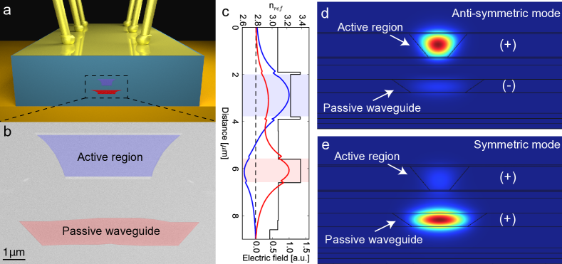
In the present work, we demonstrate dispersion compensation by coupling the optical mode to a passive dielectric waveguide engineered in the device top cladding. We fabricated a QCL based on a diagonal three quantum well design for emission at 4.6 m Yang et al. (2008); Bismuto et al. (2011). As seen in Fig. 1a, the device integrates a passive InGaAs waveguide close to the active region (see Methods for fabrication details). A Scanning Electron Micrograph (SEM) image of the device front facet is displayed in Fig. 1b. Naturally, each waveguide has a frequency-dependent propagation vector. The waveguides are designed such that these two propagation vectors are equal for a resonant frequency . At this frequency, if the two optical modes have equal group velocity dispersion (GVD), these couple to form a symmetric and an anti-symmetric supermode with resonantly depressed (respectively enhanced) GVD that can then be used for dispersion compensation Peschel, Peschel, and Lederer (1995). Applying directly such approach to a laser system leads to a fundamental difficulty: Since at resonance the supermodes are equally distributed in both waveguides, lasing can occur on the high and low GVD supermodes simultaneously.
We therefore considered a system where the two modes of the individual waveguides have a different GVD. In that case, using coupled mode theory, the induced GVD (GVD) writes as (see Supplementary materials for the derivation):
| (1) |
for the symmetric (+) and anti-symmetric (-) modes, where is the coupling strength, is the normalised frequency, the resonance bandwidth and the asymmetry factor. In the last expressions, are the group velocities and the GVDs of the decoupled active region (i=1) and passive waveguide (i=2) modes. For different from zero, the GVD difference between the two waveguides induces a shift of the GVD maxima. In turn, dispersion compensation can be achieved without requiring that the two optical modes are in resonance. The resulting asymmetry in the overlap factor of the two supermodes with the active region enables the laser to naturally select one of the two and remain monomode.
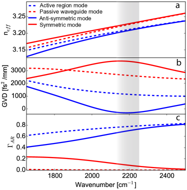
We simulated the optical modes for various geometries using a finite element solver (see Methods) and targeted zero GVD at the central laser wavelength. The refractive index profile along the growth axis of the fabricated device is displayed in Fig. 1c. The computed electric field profile of the anti-symmetric (blue line) and symmetric (red line) modes are also displayed, while the full two dimensional intensity profiles of these modes are reported in Fig. 1d and e. These two modes result from the coupling of the two distinct active region and passive waveguide optical modes with GVD = 1140 fs2/mm and = 2600 fs2/mm. The dispersion curves of the two uncoupled modes are reported in Fig. 2a with dashed lines while the dispersion of the coupled modes are reported with full lines. Our simulation predicts a minimum of the GVD close to zero at the laser operation wavelength for the anti-symmetric mode (see Fig. 2b, shaded area) and an overlap with the active region equal to 0.7 (see Fig. 2c). The latter has as a result a much larger overlap with the active region () than the symmetric mode which is localized in the passive waveguide. This induces a strong mode selection mechanism which ensures that the device operates with high efficiency on the low GVD anti-symmetric mode.
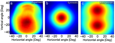
To confirm that the laser operates on the anti-symmetric mode, we measured its farfield emission profile in pulsed operation at rollover. These experimental data (see Fig. 3a) are compared to the farfield computed from the supermodes nearfield obtained from our 2D mode simulation that are displayed in Fig. 3b-c. The difference between the measured (Fig. 3a) and computed (Fig. 3c) farfield is attributed to the presence of loss and gain in the passive waveguide and active region, respectively, which is not taken into account by our model.
We measured the light and voltage versus current characteristics of the device while operated under continuous wave operation at -15 ∘C. The output power reached 75 mW at rollover (see Fig. 4a). We deduced the GVD from the subthreshold emission spectrum Hofstetter and Faist (1999) measured at a current of 450 mA at -15 ∘C. The GVD is displayed in Fig. 4b (red line). For comparison, a measurement performed on a 4.5 mm long reference device without the additional passive waveguide (see Methods for fabrication details and Supplementary Fig. 2 for full characterization) is also displayed (blue line). For the reference device, a GVD as large as 740 fs2/mm is deduced at 2200 cm-1, while for the device including the passive waveguide a GVD of only 50 fs2/mm is deduced at 2200 cm-1. This confirms that the coupling to the passive waveguide reduced the dispersion of the device (GVD = -690 fs2/mm).

To characterize the coherence of the optical spectrum we measured the intermode beatnote of the device directly from the laser bias current using a RF spectrum analyzer Villares et al. (2014) with a resolution bandwidth (RBW) of 500 Hz. Narrow beatnotes with full width at half maximum (FWHM) less than 500 Hz were measured on the whole dynamical range (see Fig. 4c and Supplementary Fig. 3). The intermode beatnote frequency tuned smoothly with current at a rate of -0.13 GHz/A, similar to values reported in Bidaux et al. (2017a). At a current of 830 mA the intermode beatnote has a FWHM 411 Hz (Fig. 4d) and the optical spectrum spans 40 cm-1 (see Fig. 4e). Such narrow and stable beatnotes have up to now always been observed in QCLs operating in comb regime.
Nevertheless, to demonstrate that the devices actually operate as frequency combs, we measured the multiheterodyne beating spectrum of two HR coated 4 mm devices at -20 ∘C. The first device current was set to 600 mA while the second device current was set to 460 mA. The optical beams were combined and focused on a MCT detector and the signal was recorded using an oscilloscope. The total acquisition time was 40 ms and the signal was averaged with a single acquisition time of 3.3 s using the method detailed in Villares et al. (2014). The resulting spectrum is displayed in Fig. 4f. Ninety three distinct comb lines are observed. Since the free spectral range of the combs is approximately 0.39 cm-1, this corresponds to an optical span of 38 cm-1 and demonstrates that the devices operate as frequency combs on the whole spectral bandwidth. The FWHM of one line is 1.26 MHz (see Fig. 4g), this directly shows the suitability of these devices for dual-comb spectrometers in the first atmospheric window.
In conclusion, we presented a dual coupled-waveguide design for dispersion compensation in semiconductor lasers and demonstrated its application to a quantum cascade laser. The fabricated devices operate as frequency combs on the whole spectral bandwidth and dynamical range. Unlike previously demonstrated integrated dispersion compensation methods, the dual waveguide scheme can be applied to various types of semiconductor lasers and material systems. Moreover, it allows to correct for GVD values up to a few thousand fs2/mm. This suggests that this design strategy could enable the development of high performance semiconductor laser based optical frequency combs from the long mid-infrared to the near-infrared wavelengths ranges. Actually, an interband laser waveguide design that is computed to be dispersion compensated at 1.3 m is proposed in the supplementary material.
Methods
Devices fabrication
The active region of the device including coupled-waveguides was grown by molecular beam epitaxy using the InGaAs/AlInAs material system on an InP:Si (2 x 1017 cm-3) substrate. The active layers were placed between two 100 nm thin layers of Si-doped InGaAs (6 x 1016 cm-3). The exact layers sequence of the QCL is detailed in Yang et al. (2008). The device was processed to a buried heterostructure QCL. A 4.4 m wide ridge was etched by wet-etching technique and a lateral InP:Fe insulating layer was grown by metalorganic vapour phase epitaxy (MOVPE). The top cladding layers were then grown by MOVPE and include an InGaAs waveguiding layer. The top cladding layers sequence is 0.5 m InP:Si 1 x 1017 cm-3, 1.2 m InP:Si 1 x 1016 cm-3, 1 m InGaAs:Si 1 x 1016 cm-3, 1.6 m InP:Si 1 x 1016 cm-3, 0.4 m InP:Si 2 x 1017 cm-3, 0.4 m InP:Si 3 x 1018 cm-3. A second 6.7 m wide ridge was etched in the cladding by wet-etching and a lateral InP:Fe insulating layer was grown by MOVPE. For the reference device the top cladding layers sequence is: 0.42 m InP:Si 1 x 1017 cm-3, 2.5 m InP:Si 1 x 1016 cm-3, 0.85 m InP:Si 1 x 1018 cm-3. Devices were mounted episide down on AlN submounts.
Optical mode simulation
We performed two-dimensional finite-element simulations of the waveguide structure using the commercially available software Comsol Multiphysics. The intrinsic refractive indices were obtained from Pikhtin and Yas’kov formula using the parameters given in Palik and Ghosh (1998). The doped refractive indices are deduced using Drude model. We assume a collision time of 100 fs and effective masses of 0.073 me for InP and 0.043 me for InGaAs.
References
- Derickson et al. (1992) D. J. Derickson, R. J. Helkey, A. Mar, J. R. Karin, J. G. Wasserbauer, and J. E. Bowers, “Short pulse generation using multisegment mode-locked semiconductor lasers,” IEEE Journal of Quantum Electronics 28, 2186–2202 (1992).
- Avrutin, Marsh, and Portnoi (2000) E. Avrutin, J. Marsh, and E. Portnoi, “Monolithic and multi-GigaHertz mode-locked semiconductor lasers: Constructions, experiments, models and applications,” IEE Proceedings - Optoelectronics 147, 251–278 (2000).
- Keller and Tropper (2006) U. Keller and A. C. Tropper, “Passively modelocked surface-emitting semiconductor lasers,” Physics Reports 429, 67–120 (2006).
- Rafailov, Cataluna, and Sibbett (2007) E. U. Rafailov, M. A. Cataluna, and W. Sibbett, “Mode-locked quantum-dot lasers,” Nature photonics 1, 395–401 (2007).
- Hugi et al. (2012) A. Hugi, G. Villares, S. Blaser, H. C. Liu, and J. Faist, “Mid-infrared frequency comb based on a quantum cascade laser,” Nature 492, 229–233 (2012).
- Palik and Ghosh (1998) E. D. Palik and G. Ghosh, eds., Handbook of optical constants of solids (Academic Press, San Diego, 1998).
- Villares et al. (2016) G. Villares, S. Riedi, J. Wolf, D. Kazakov, M. J. Süess, P. Jouy, M. Beck, and J. Faist, “Dispersion engineering of quantum cascade laser frequency combs,” Optica 3, 252 (2016).
- Kim, Choi, and Delfyett (2006) J. Kim, M.-T. Choi, and P. J. Delfyett, “Pulse generation and compression via ground and excited states from a grating coupled passively mode-locked quantum dot two-section diode laser,” Applied Physics Letters 89, 261106 (2006).
- Diddams (2010) S. A. Diddams, “The evolving optical frequency comb [Invited],” Journal of the Optical Society of America B 27, B51 (2010).
- Keilmann, Gohle, and Holzwarth (2004) F. Keilmann, C. Gohle, and R. Holzwarth, “Time-domain mid-infrared frequency-comb spectrometer,” Optics letters 29, 1542–1544 (2004).
- Rösch et al. (2014) M. Rösch, G. Scalari, M. Beck, and J. Faist, “Octave-spanning semiconductor laser,” Nature Photonics , 42–47 (2014).
- Burghoff et al. (2014) D. Burghoff, T.-Y. Kao, N. Han, C. W. I. Chan, X. Cai, Y. Yang, D. J. Hayton, J.-R. Gao, J. L. Reno, and Q. Hu, “Terahertz laser frequency combs,” Nature Photonics 8, 462–467 (2014).
- Villares et al. (2014) G. Villares, A. Hugi, S. Blaser, and J. Faist, “Dual-comb spectroscopy based on quantum-cascade-laser frequency combs,” Nature Communications 5, 5192 (2014).
- Yang et al. (2016) Y. Yang, D. Burghoff, D. J. Hayton, J.-R. Gao, J. L. Reno, and Q. Hu, “Terahertz multiheterodyne spectroscopy using laser frequency combs,” Optica 3, 499 (2016).
- Westberg, Sterczewski, and Wysocki (2017) J. Westberg, L. A. Sterczewski, and G. Wysocki, “Mid-infrared multiheterodyne spectroscopy with phase-locked quantum cascade lasers,” Applied Physics Letters 110, 141108 (2017).
- Lu et al. (2017) Q. Y. Lu, S. Manna, S. Slivken, D. H. Wu, and M. Razeghi, “Dispersion compensated mid-infrared quantum cascade laser frequency comb with high power output,” AIP Advances 7, 045313 (2017).
- Riemensberger et al. (2012) J. Riemensberger, K. Hartinger, T. Herr, V. Brasch, R. Holzwarth, and T. J. Kippenberg, “Dispersion engineering of thick high-Q silicon nitride ring-resonators via atomic layer deposition,” Optics Express 20, 27661 (2012).
- Okawachi et al. (2014) Y. Okawachi, M. R. E. Lamont, K. Luke, D. O. Carvalho, M. Yu, M. Lipson, and A. L. Gaeta, “Bandwidth shaping of microresonator-based frequency combs via dispersion engineering,” Optics Letters 39, 3535 (2014).
- Peschel, Peschel, and Lederer (1995) U. Peschel, T. Peschel, and F. Lederer, “A compact device for highly efficient dispersion compensation in fiber transmission,” Applied Physics Letters 67, 2111 (1995).
- Bidaux et al. (2017a) Y. Bidaux, I. Sergachev, W. Wuester, R. Maulini, T. Gresch, A. Bismuto, S. Blaser, A. Muller, and J. Faist, “Plasmon-enhanced waveguide for dispersion compensation in mid-infrared quantum cascade laser frequency combs,” Optics Letters 42, 1604 (2017a).
- Jouy et al. (2017) P. Jouy, J. M. Wolf, Y. Bidaux, P. Allmendinger, M. Mangold, M. Beck, and J. Faist, “Dual comb operation of 8.2 m Quantum Cascade Laser frequency comb with 1 W optical power,” Applied Physics Letters 111, 141102 (2017).
- Bidaux et al. (2017b) Y. Bidaux, K. A. Fedorova, D. A. Livshits, E. U. Rafailov, and J. Faist, “Investigation of the chromatic dispersion in two-section InAs/GaAs quantum-dot lasers,” IEEE Photonics Technology Letters 29, 2246 – 2249 (2017b).
- Yang et al. (2008) Q. Yang, R. Lösch, W. Bronner, S. Hugger, F. Fuchs, R. Aidam, and J. Wagner, “High-peak-power strain-compensated GaInAs/AlInAs quantum cascade lasers (λ 4.6 m) based on a slightly diagonal active region design,” Applied Physics Letters 93, 251110 (2008).
- Bismuto et al. (2011) A. Bismuto, R. Terazzi, M. Beck, and J. Faist, “Influence of the growth temperature on the performances of strain-balanced quantum cascade lasers,” Applied Physics Letters 98, 091105 (2011).
- Hofstetter and Faist (1999) D. Hofstetter and J. Faist, “Measurement of semiconductor laser gain and dispersion curves utilizing Fourier transforms of the emission spectra,” IEEE Photonics Technology Letters 11, 1372–1374 (1999).
Acknowledgements
The authors would like to thank Dmitry Kazakov and Matthew Singleton for careful reading of the paper and fruitful discussions. This work was supported by the Swiss National Science Fundation (SNF) and by DARPA under the SCOUT program.
Authors contributions
Y.B. developed the simulations, designed the waveguide, performed experiments, analysed data and wrote the manuscript. F.K. fabricated the coupled-waveguide quantum cascade lasers, performed experiments and analysed data. P.J. fabricated the reference quantum cascade lasers, performed experiments and analysed data. M.B. grew the quantum cascade laser material. J.F. proposed the experiment, analysed data and supervised the work.