Current address: ]Center for NanoScience & Fakultät für Physik, LMU-Munich, 80539 München, GermanyCurrent address: ]Weierstraß-Institut für angewandte Analysis und Stochastik, Mohrenstr. 39, 10117 Berlin, Germany
Optimization of ohmic contacts to n-type GaAs nanowires
Abstract
III-V nanowires are comprehensively studied because of their suitability for optoelectronic quantum technology applications. However, their small dimensions and the spatial separation of carriers from the wire surface render electrical contacting difficult. Systematically studying ohmic contact formation by diffusion to -doped GaAs nanowires, we provide a set of optimal annealing parameters for Pd/Ge/Au ohmic contacts. We reproducibly achieve low specific contact resistances of at room temperature becoming an order of magnitude higher at K. We provide a phenomenological model to describe contact resistances as a function of diffusion parameters. Implementing a transfer-matrix method, we numerically study the influence of the Schottky barrier on the contact resistance. Our results indicate that contact resistances can be predicted using various barrier shapes but further insights into structural properties would require a full microscopic understanding of the complex diffusion processes.
I Introduction
GaAs nanowires -doped with silicon (-GaAs) are promising building blocks for optoelectronic devices such as light emitting diodes (LEDs) and photovoltaic cells or for future quantum technology applications Yan, R. and Gargas, D. and Yang, P. (2009); Czaban et al. (2009); Tomioka et al. (2010); Gutsche et al. (2011); Chuang et al. (2011); Borgström et al. (2011); Mariani et al. (2011); Krogstrup et al. (2013); Song et al. (2014); Miao et al. (2014); Orrù et al. (2014); Dasgupta et al. (2014); Dimakis et al. (2014); Koblmüller et al. (2017). For applications requiring charge transport or the integration into device circuitry, nanowires have to be electrically contacted Gutsche et al. (2011); Krogstrup et al. (2013); Song et al. (2014); Miao et al. (2014); Orrù et al. (2014). To achieve optimal device performance, their contacts should have a small and current independent resistance, resembling ohmic contacts. This imposes a challenge, as the band bending at metal-to-semiconductor contacts leads to Schottky barriers Schottky (1939) reducing the carrier transmission and causing non-linear current-voltage (-) characteristics. A Schottky barrier forms by charge transfer between the semiconductor and the metal surface driven by the equalization of the chemical potentials of the materials at the interface. This process results in a charge depletion zone in the semiconductor Tung (2014); Sze and Ng (2007). The width of the depletion zone defines the Schottky barrier width . It depends on the concentration of free charge carriers in the semiconductor, governed by the doping concentration , such that . It can be tuned by doping, as increasing decreases which enhances the transmission through the barrier by quantum tunneling. The barrier height is a material-dependent constant which is related to the difference between the work function of the metal and the electron affinity of the semiconductor but, practically, strongly depends on defect states at the interface. Many applications require weak doping of semiconductors which yields wide Schottky barriers. Unfortunately, such a wide barrier corresponds to a large specific contact resistance of typically or higher, even at room temperature. However, the specific contact resistance can be dramatically reduced and - characteristics resembling ohmic behavior can be obtained by enhancing the doping locally, near the interface. An alternative way to reduce the absolute contact resistance would be to increase the lateral extension of the contact region. This possibility is, however, limited if small nanostructures such as thin and short nanowires have to be contacted.
Low resistance ohmic contacts to planar -GaAs wafers are frequently achieved by local diffusion of germanium (Ge) atoms into the semiconductor using rapid thermal annealing (RTA) Kim and Holloway (1997). The detailed kinetics of such a diffusion process is material dependent, complex, and –in most practical cases– not well understood. Consequently, optimizing contacts is often based on a trial-and-error approach. Improved contacts to -GaAs had been achieved by adding a thin layer of palladium (Pd) placed between the GaAs surface and the Ge layer, where the Pd acts like a catalyst promoting the aspired diffusion of germanium into GaAs Marshall et al. (1987). The specific diffusion process was described phenomenologically by a regrowth model Kim and Holloway (1997). In a nutshell, the Pd enables out-diffusion of Ga from the GaAs wafer before it quickly diffuses through the Ge layer away from the GaAs surface Tahini et al. (2015). The Ge atoms then diffuse into the gallium vacancies below the GaAs wafer surface.
Yielding low-resistive ohmic contacts to GaAs nanowires Gutsche et al. (2011); Orrù et al. (2014) is generally more difficult than to bulk GaAs crystals because small wires allow only for small contact areas. In addition, their quasi one-dimensional geometry with a high surface-to-volume ratio alters the diffusion dynamics in nanowires compared to bulk material. A more aggressive diffusion (e.g. at higher temperature), which in the case of bulk crystals often yields success, likely compromises the properties and functionality of the nanowire itself by excessive in-diffusion of Ge (away from the contacts) or even deterioration of the wire between the contacts (e.g. by evaporation of arsenic). Consequently, creating ohmic contacts to nanowires requires a particularly high level of control of the diffusion dynamics. The most successful approach to create ohmic contacts to -GaAs nanowires so far is based on thermal annealing of layers of Pd, Ge and a capping layer of gold (Pd/Ge/Au) locally evaporated onto the wire Gutsche et al. (2011). In the present work we performed an optimization of similar Pd/Ge/Au contacts by systematically exploring the annealing parameters: temperature and duration. Our wires have an undoped GaAs core covered by an -doped GaAs shell. We achieved record low resistive ohmic contacts and confirm the enhanced quantum tunneling through the Schottky barriers with reduced width by transport measurements at liquid-helium temperatures.
Our systematic experimental results allow for a quantitative comparison with a phenomenological model, which describes the transmission through Schottky barriers as a function of diffusion parameters. Owing to a lack of knowledge regarding the detailed diffusion kinetics, we radically simplify our model to a single-stage process described by Fick’s laws. As a consequence, we cannot predict the realistic shape of the Schottky barrier. As a way out, we model various barrier shapes. We find that the measured contact resistances can be predicted independent of the details of the Schottky barrier while it is impossible to extract microscopic details such as the Schottky barrier shape or diffusion parameters from our transport data. This would require a full understanding of the complex (multistep) microscopic diffusion dynamics.
II Experimental Details
We have fabricated GaAs wires by Ga-assisted molecular beam epitaxy on a silicon (111) substrate covered by native oxide. After growing the m long and nm wide undoped GaAs cores at C, we added a nm thick silicon-doped shell by lateral growth at C, see Refs. Küpers et al. (2017); Dimakis et al. (2012) for details. The nominal doping concentration in the shell is , determined for similar samples. For our transport experiments, we transferred the wires after growth (solute in isopropanol) to an -doped silicon wafer, which is used as an electrical field effect back gate at the same time. To isolate the wires from the back gate, the wafer is covered with 50 nm thermal oxide. For the fabrication of the Pd/Ge/Au contacts to the nanowire, we used optical lithography. After development the samples were cleaned in a HCl:H2O solution at the ratio 1:200 for 20 s, afterwards rinsed in DI water, blown dry with N2 and loaded promptly into an electron-beam evaporation chamber. Within the load lock of the evaporation chamber, we applied three minutes of Argon-ion sputtering at 36 eV. This way the native oxide is removed from the sample, where not covered by resist, including the nanowire surface at the contact positions. Finally, the metal layers, namely 50 nm of Pd, 170 nm of Ge, and 80 nm of Au, were deposited followed by a metal lift-off process. In Fig. 1,
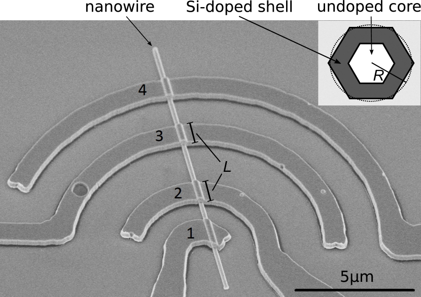
we present a scanning electron microscope (SEM) image of a typical wire with four contacts.
Aiming at quantum applications, we are interested in the low-power properties of the nanowires. Consequently, we characterized the nanowires by measuring - curves for mV employing both, two-terminal (2TM) and four-terminal (4TM) transport measurements. In our 2TM measurements we applied a constant voltage between the inner contacts, 2 and 3, see Fig. 1, and measured current using a current voltage amplifier. In our 4TM measurements we applied a constant between the outer contacts, 1 and 4, and measured between the inner contacts. Assuming that the 4TM resistance represents the nanowire resistance between the inner contacts and neglecting much smaller lead resistances, we can express the average of the two contact resistances (at contacts 2 and 3) as . Evaporation of the contacts onto a hexagonal shaped nanowire suffers from a shadowing effect such that in our case only roughly 50% of the nanowire circumference is actually in direct contact with the contact material. Under this assumption, we can estimate the specific contact resistance as , where nm and m are the nominal radius of the wire and width of our contacts, respectively.
For comparison, we measured the 2TM and 4TM - characteristics before and after diffusion of the contacts by RTA in a furnace with electrical heating and nitrogen flow cooling such that the heating and cooling rates where roughly equal and constant at K/s, as sketched in Fig. 2.

To systematically study the diffusion process, we varied the annealing time and temperature for various samples.
III Experimental Results
In Fig. 3(a),
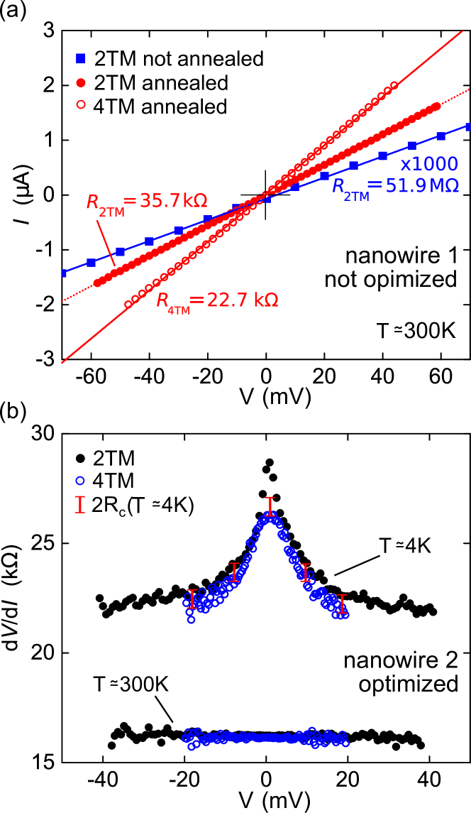
we show typical - curves resulting from 2TM and 4TM measurements at room temperature. All curves origin from the same nanowire. Before RTA (not annealed), is entirely dominated by the contacts. After not yet optimized annealing at C for s, the contact resistance drops by a factor of 4000 to , while the nanowire resistance stays unaffected at ( before annealing is not shown). In order to determine the parameters for an optimal annealing procedure, we carried out a systematic investigation. Before discussing details, we present in Fig. 3(b) the characteristics after optimal annealing. The figure includes 2TM and 4TM measurements at both, cryogenic and room temperature. To reveal more details, here we plot the differential resistance, i.e. the derivative of - curves, instead of current versus voltage. The constant value of at K corresponds to a linear - characteristic and we find very low contact resistances of . Upon cooling to K in a liquid helium bath, the wire resistance () as well as the contact resistances increase 111This increase of contact resistances while lowering the temperature is an intrinsic feature of a Schottky barrier. It reflects the energy dependence of transmission through a barrier of finite height and has been previously discussed in terms of a transition from classical thermionic emission to quantum mechanical field emission Kim and Holloway (1997); Tung (2014). Our model reflects the temperature dependence by integrating over the carrier excitation spectrum in the leads, see Appendix for details.. Nevertheless, we have achieved contact resistances which are even at cryogenic temperatures an order of magnitude lower than our wire resistances and, importantly, much lower than the fundamental one-dimensional resistance quantum of . Such low contact resistances would allow for ballistic quantum transport measurements.
The low-temperature measurements reveal a slightly non-ohmic characteristics at low energies: at 4.2 K the nanowire resistance increases by 18% as is decreased from 20 mV to zero. We interpret this behavior as a signature of disorder in our wires, which causes hopping transport (caused by disorder-induced barriers) at cryogenic temperatures. This excludes the possibility of ballistic linear-response transport in these specific wires. Interestingly, we find a particularly strong increase of compared to for very small mV, visible as a sharp maximum of the low temperature , black dots in Fig. 3(b). While this observation requires further investigation, it might be attributed to a disorder potential increasing the effective Schottky barrier width at low energies, i.e. for . We expect that disorder-free nanowires would allow for ohmic - characteristics at cryogenic temperatures and very low energies 222Disorder in our specific nanowires can be caused by polytypism or surface states, but it is likely dominated by the Coulomb potential of donor ions as the free carriers reside in the same material layer..
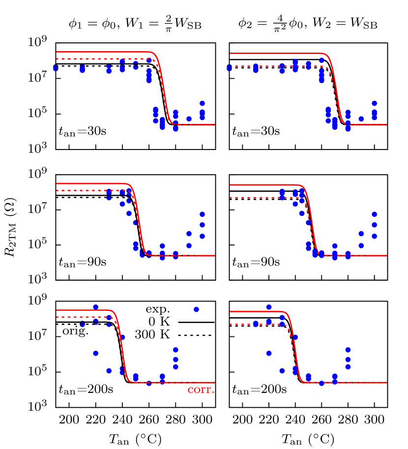
Searching for the optimal annealing procedure, we systematically varied the RTA temperature and duration . In Fig. 4,
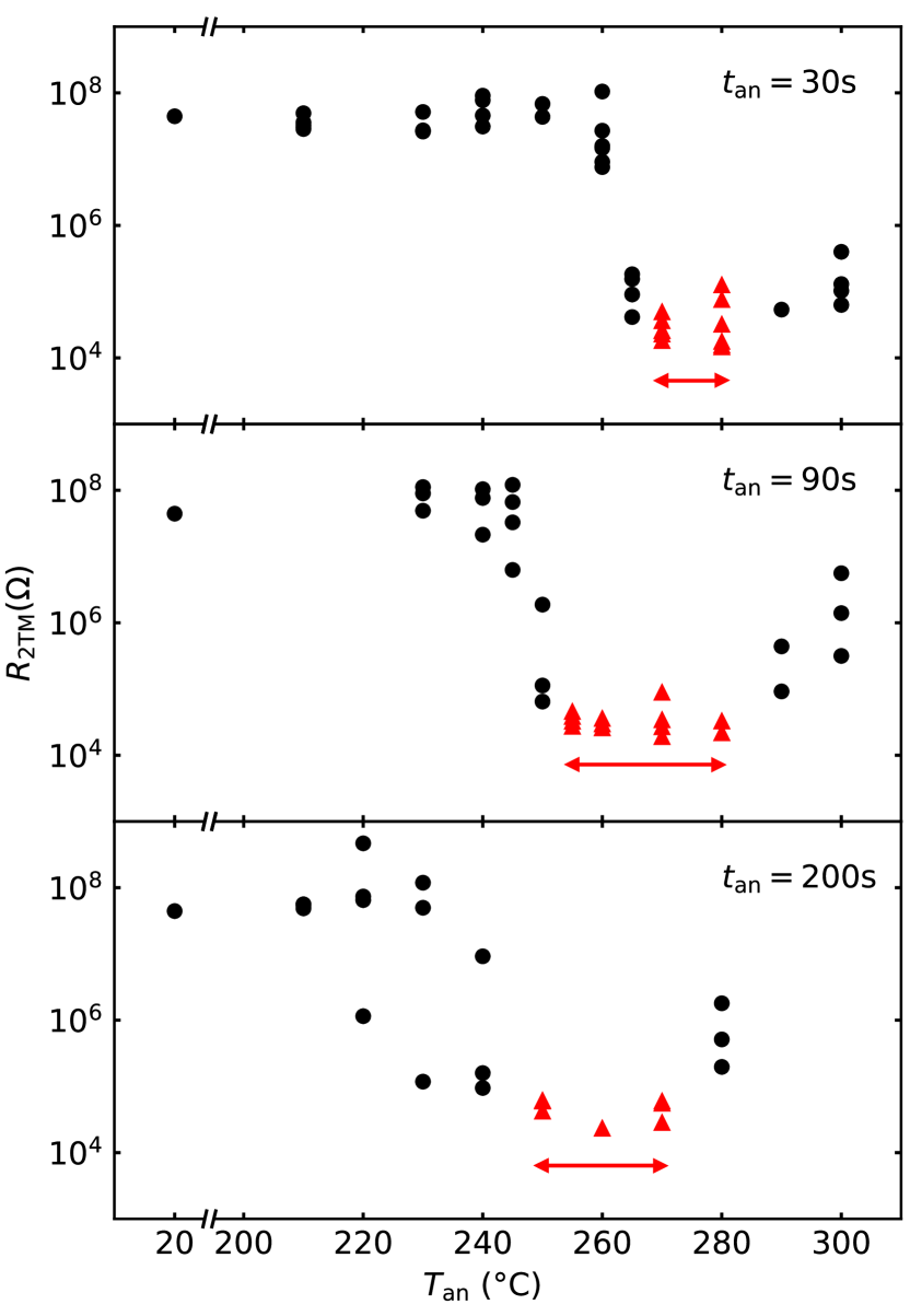
we present the resulting for three different , all measured at room temperature. The highest measured resistances of correspond to contacts before annealing. The lowest measured resistances of are dominated by the nanowire resistance and correspond to contact resistances of . We generally observe a rapid drop in contact resistance as is increased, where the drop happens at higher temperature for shorter annealing duration, in qualitative agreement with Fick’s diffusion laws. Importantly, on the one hand, faster annealing at higher temperature yields more reproducible results within the relevant range of parameters. (The scattering of near the drop increases for longer .) On the other hand, as is increased beyond C, the measured resistance grows again. We believe that this resistance increase is related to evaporation of arsenic at high temperatures which can cause a structural deterioration of the nanowires Gutsche et al. (2011). SEM images presented in Fig. 5
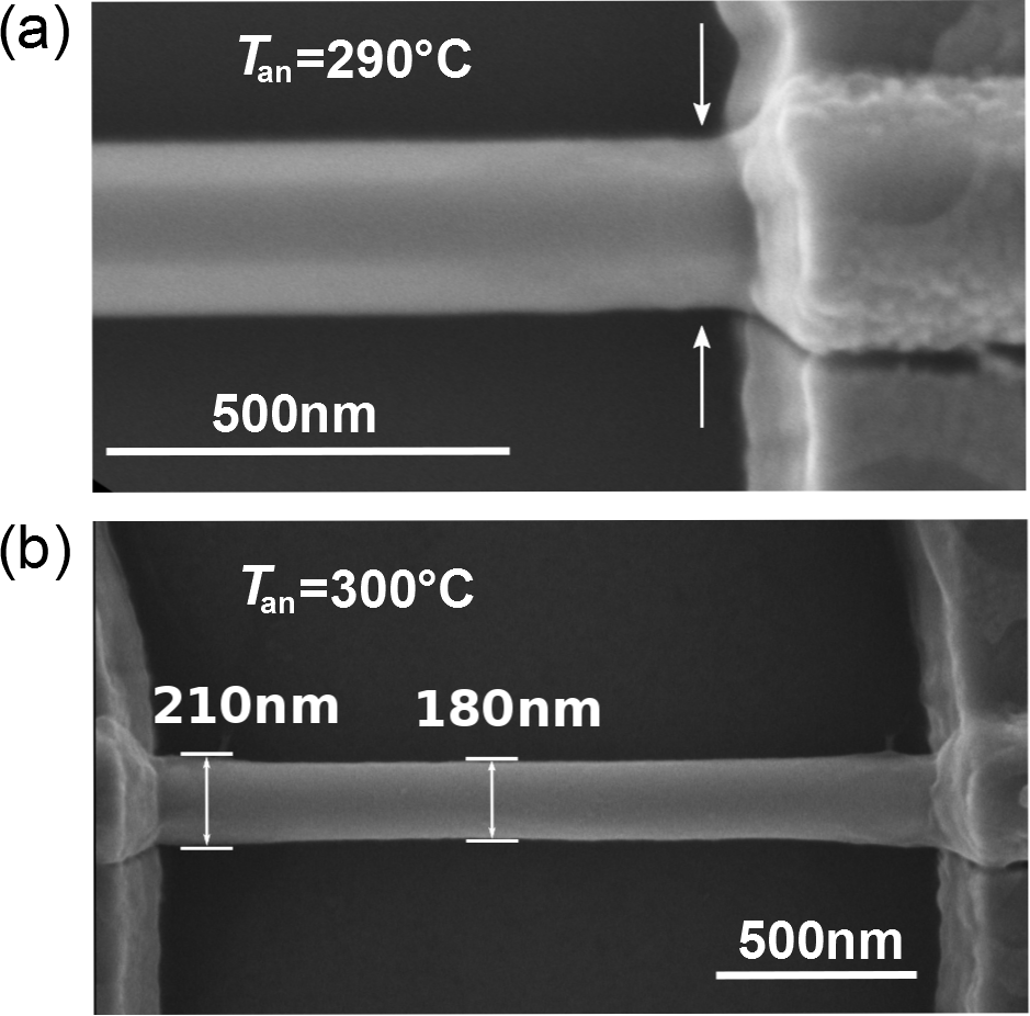
support our explanation 333In our transport measurements as well as in energy dispersive X-ray spectroscopy (EDX) measurements (not shown) we find no indications of an enhanced germanium concentration in the nanowires away from the contact areas..
As a result, the optimal range for RTA, which is indicated in Fig. 4 by red double arrows, is limited by the initial resistance drop from low and the final resistance increase at high . It is immediately evident, that our intermediate s allows for the largest temperature window which promises lowest possible contact resistances.
IV Model
In the following, we develop a phenomenological model to describe the (room temperature) contact resistance as a function of annealing parameters . The purpose of the model is to provide additional understanding and help us to further improve the contacts to III-V nanowires. The model consists of two steps: first, the identification of the donor distribution after annealing which determines the width of the Schottky barrier and, second, the computation of the resistance of the Schottky barrier, i.e. the contact resistance.
The diffusion dynamics in our layered system containing several materials is very complicated and goes beyond the scope of the present paper. Here, we radically simplify the complex dynamics by assuming a one-dimensional diffusion process of Ge into the semiconductor described by Fick’s laws. Our simplified one-dimensional diffusion model is illustrated in Fig. 6.
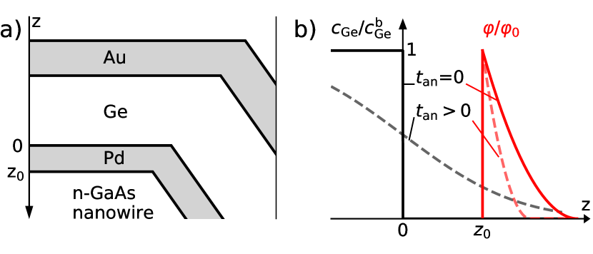
Using separate half spaces as initial condition before annealing, we assume the initial () concentration distribution and with being the bulk atomic concentration within the layer of pure Ge, see Fig. 6(a). Applying Fick’s laws we model the Ge concentration near the nanowire surface as a function of diffusion depth , annealing time , and annealing temperature as Gottstein (2007)
| (1) |
where and denote the diffusion coefficient and hopping activation energy, respectively. The nanowire doping concentration predicted by Eq. (1) is then
| (2) |
assuming that every incorporated Ge atom and every Si atom act equally as one donor atom 444Note, that we neglect compensation effects which can arise if e.g. a fraction of silicon dopants act as acceptor instead of donor. It has been shown, that such compensation effects are minimal in our core-shell wires Dimakis et al. (2012)..
As a consequence of the above simplification for the diffusion dynamics, we cannot predict the realistic microscopic donor distribution in detail. Consequently, the shape of the Schottky barrier is also not precisely known. As hinted above, this limitation is very common and, in particular, applies to nanostructures with Schottky barriers fabricated by local diffusion. In order to estimate the consequences of an unknown Schottky barrier shape and to determine the relevance of a specific shape for the physical predictions of a model, we calculate the transmission for various barrier shapes.
In our first calculation, we follow the standard approach by assuming a uniform using with nm as a reference depth in Eq. (1). Furthermore, we neglect screening effects such that the Schottky barrier takes its text book shape
| (3) |
for and elsewhere and with the barrier width determined by
Here, and are the dielectric constant of vacuum and GaAs, respectively, while is the elementary charge. The barrier height is, in first approximation, a material constant independent of , hence independent of the detailed barrier shape.
To capture thermally activated hopping over the barrier as well as quantum tunneling, the transmission through a Schottky barrier, described by Eq. (3), is traditionally approximated in terms of three separate contributions: thermionic emission, field emission, and thermionic field emission Sah (1991); Kim and Holloway (1997); Sze and Ng (2007). The accuracy of this semiclassical approach is hard to predict away from the extreme limits (deep classical or quantum limit). For these limits, the barrier shape does not matter. For the case of a (truncated) parabolic barrier, the exact transmission can be calculated analytically, which was suggested as a possible route to approximate the transmission through realistic Schottky barriers Hansen and Brandbyge (2004). Instead, we calculate numerically the full transmission for arbitrary barrier shapes. Our analysis below shows that physical predictions require knowledge of the realistic barrier shape.
Implementing a transfer-matrix method (TMM) Tsu and Esaki (1973), we have evaluated the contact resitance for four different shapes of the Schottky barrier, as illustrated in the insets of Fig. 7.
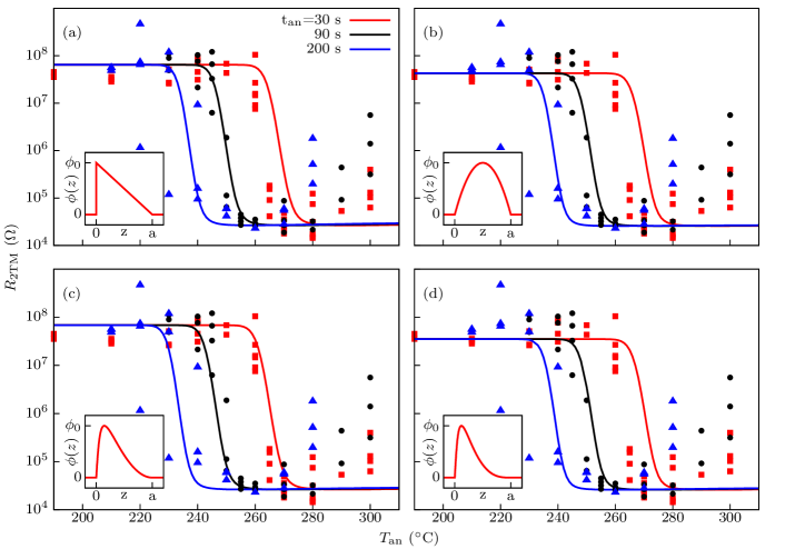
A detailed description of the numerical model is given in the Appendix. Our first example is a simple triangular potential, . The second example is a parabolic barrier with maximum at a/2, . As the parabolic barrier allows for an analytical calculation Hansen and Brandbyge (2004), we take it as a reference to verify our numerical calculations, as discussed in the Appendix. Next, we have assumed half of a parabola with a maximum softened by an arctangent function, . This potential shape is very close to (albeit more realistic than) the Schottky barrier for a homogeneous carrier distribution described by Eq. (3). Finally, to account for the expected decrease of the donor concentration away from the nanowire surface as predicted by Eq. (1), we have employed a steeper potential resembling half a cubic parabola with a softened maximum, . We expect the last one to describe the most realistic barrier shape.
The simulation parameters, i.e. height of the Schottky barrier , activation energy , and the diffusion constant are not well known. Together, they define the barrier width , assuming via Eqs. (1)–(3). We determine these parameters from a least-squares fit of the simulations to measured 2TM resistances, . In Fig. 7 we present the calculated curves in comparison to our measured data points already seen in Fig. 4. For our calculations we used with nm, which is the thickness of the palladium layer, as germanium has to pass the palladium before diffusing into the GaAs nanowire. This choice reflects the simplification of a complex diffusion process to a one-dimensional model described by Fick’s laws. A different will change the absolute values of and , but does not affect their relative changes and our main conclusions. The parameters thus obtained by fitting the four potential shapes are listed in Tab. 1.
| (meV) | (eV) | (m2/s) | |
|---|---|---|---|
| 679 | 1.440 | 8.4610-5 | |
| 583 | 1.442 | 7.9210-5 | |
| 781 | 1.408 | 5.1010-5 | |
| 816 | 1.440 | 7.4210-5 |
While remains quite similar for all potential shapes under consideration, and exhibit stronger variations. As demonstrated in Fig. 7 within the measurement accuracy our model captures the measured two-terminal resistance as a function of annealing temperature and time correctly, independent of the details of the Schottky barrier shapes. As a result, the specific shape of the Schottky barrier clearly cannot be concluded from our simulations.
The reduction of observed with increased in Figs. 4 and 7 reflects the dependence of the barrier width WSB on and tan [also see discussion of Fig. 4 above]. Our model curves capture the resitance drop by more than three orders of magnitude and the dependence of this drop on both, the annealing temperature and duration correctly. This supports our procedure of simplifying a complex diffusion process by Fick’s laws. A detailed physical understanding beyond our analysis, a prediction of the contact resistance, or a prediction of the perfect annealing parameters would require the knowledge of the exact shape of the Schottky barrier. However, if such an insight can be achieved, the TMM is a reliable and computationally efficient method to provide further quantitative information, e.g. on the barrier width and height, which then could lead to a further optimization of the electrical contacts to nanowires.
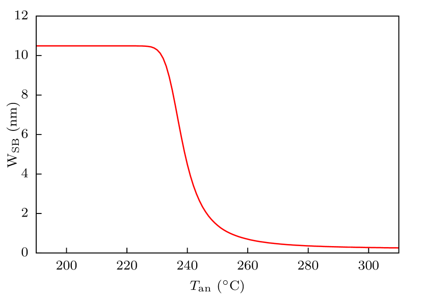
For completeness, we present the Schottky barrier width dependence on annealing temperature in Fig. 8
V Summary
We studied the effect of annealing parameters on the formation of ohmic contacts to GaAs nanowires and thereby minimized the contact resistance. Our procedure allows to systematically and reliably optimize ohmic contacts by diffusion and can be applied to arbitrary nanostructures. We developed a phenomenological model describing the formation of a Schottky barrier by donor diffusion and determining the transmission through the barrier using the transfer-matrix method. The latter accurately describes our data independent of the shape of the Schottky barrier. In order to precisely predict physical parameters it would be necessary to know the shape of the barrier, which –in turn– would require a detailed understanding of the complex diffusion processes on a microscopic level.
VI Acknowledgments
We would like to acknowledge technical help from Walid Anders, Anne-Kathrin Bluhm, Uwe Jahn, Angela Riedel and Werner Seidel.
VII Appendix
Numerical transfer matrix method
A particle with energy is transmitted from left to right through a barrier with transmission . We begin with considering the one-dimensional problem and thereby omit the time dependence, which is not relevant for our problem. The wave function of the particle impinging the barrier from the left is then , which is partially reflected to the left with amplitude and transmitted to the right side of the barrier with . The relationship between and wave numbers can be found by substituting these wave functions into the time independent Schrödinger equation
With and denoting the values of the potential at the left and right side of the barrier we find
where is the effective mass which we assume to be constant, resembling the parabolic band approximation. To determine the wave function for a finite barrier of arbitrary shape between and , we predefine the value of the wave function at to be unity and calculate its corresponding derivative
As the next step, we numerically integrate the Schrödinger equation from to , while the wave function and its derivative need to satisfy
such that
To complete the one-dimensional problem, we numerically calculate the reflection and transmission coefficients and using
We calculate the one-dimensional transmission because only momentum components perpendicular to the barrier contribute. Still, to determine the realistic transmission in three dimensions, we have to factor in the three-dimensional dispersion relation of the impinging electrons Hansen and Brandbyge (2004). First, we calculate the three-dimensional partial transmission at a given energy by numerically integrating
| (4) |
with the applied voltage and the kinetic energy component of electrons corresponding to their initial motion in the direction. To determine the full three-dimensional transmission we have to integrate over all relevant energies. We first calculate the transmission at zero temperature
and then, using the Sommerfeld expansion valid for Ashcroft and Mermin (1976), the lowest order correction term for a finite temperature
such that
After numerically computing
we calculate the linear-response two-terminal resistance with
| (5) |
where
Here, is the conductance quantum, the radius of the NW and the contact width along the NW, while is the Fermi wavelength (cf. Tab. 2).
| parameter | value | parameter | value |
| () | 0.067 | (eV-1) | 27.0794 |
| (meV) | 14.0 | (nm) | 24 |
| (nm) | 13.0 | (nm) | 90 |
| (eV) | 1.0 | (m) | 1 |
| (V) | 0.01 .. 1 | (k) | 25 |
| (m2/s) | 10-4 | (eV) | 1.445 |
| (m-3) | 91024 | (m-3) | 4.421028 |
| (nm) | 50 | 13.18 |
We declared convergence to be achieved for mV. To simulate Schottky barriers in the present work, we assumed the nominal Schottky barrier width to be equal to the actual barrier width .
Analytical solution for a parabolic barrier
The transmission through a parabolic barrier of the form can be calculated analytically, which we have used to verify the correctness of our numerical calculations. We follow the approach of Hansen and Brandbyge Hansen and Brandbyge (2004), but demonstrate that a term omitted in their calculation becomes relevant for small Fermi energies typical for doped semiconductors. We have to solve the integral in Eq. (4) to obtain the partial transmission , where we take from Eq. (19) in Ref. Hansen and Brandbyge (2004)
| (6) |
Here, we define as in Fig. 2 of Ref. Hansen and Brandbyge (2004) to be positive. We obtain:
where the term omitted in Eq. (21) of Ref. Hansen and Brandbyge (2004) is marked red and
To obtain the resistance at zero temperature, we compute
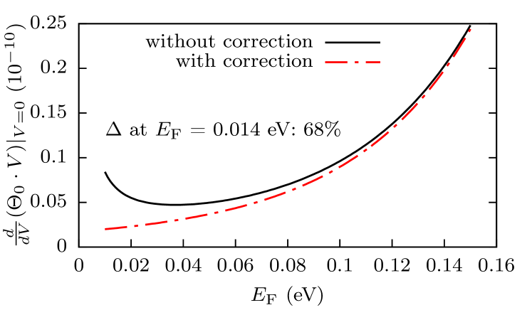
| (7) |
In Fig. 9 we evaluate the impact of the neglected term in Ref. Hansen and Brandbyge (2004) (second line, red) by plotting as a function of the Fermi energy . While omitting the red terms yields a good approximation above a Fermi energy of about 100 meV, the correct value of is almost 70% smaller at the Fermi energy of 14 meV in our nanowires. All other parameters required for this comparison are listed in Tab. 2. Omitting the correction term, as proposed in Ref. Hansen and Brandbyge (2004) clearly yields an incorrect description of our system.
In the following, we approximate the Schottky barrier with barriers of parabolic shape in order to use the formalism introduced by Hansen and Brandbyge. For a comparison, we keep either {1} the barrier height or {2} the barrier width unchanged and adjust the other parameter to keep the tunnel probability at fixed Fermi energy. The width depends on the Ge concentration according to Eq. (3) which, in turn, is a function of the annealing temperature as shown in Fig. 8. The barriers are approximated as
| (9) |
for {1} and as
| (10) |
for {2}. The respective heights and widths of the two parabolic barriers are
| (11) |
| (12) |
Replacing and in Eq. (7) with
| (13) |
and , respectively, we compute the 2TM linear-response resistance R of the nanowire and two contacts using Eq. (5). In Fig. 10 we present the calculated as a function of the annealing temperature for different annealing times for the two parabolic barriers with and without the correction terms in Eq. (7). For a direct comparison we also plot the measured .
References
- Yan, R. and Gargas, D. and Yang, P. (2009) Yan, R. and Gargas, D. and Yang, P. “Nanowire photonics” Nature Photonics 3, 569 (2009).
- Czaban et al. (2009) J. A. Czaban, D. A. Thompson, and R. R. LaPierre “GaAs Core-Shell Nanowires for Photovoltaic Applications” Nano Letters 9 (1), 148 (2009).
- Tomioka et al. (2010) K. Tomioka, J. Motohisa, S. Hara, K. Hiruma, and T. Fukui “GaAs/AlGaAs Core Multishell Nanowire-Based Light-Emitting Diodes on Si” Nano Letters 10 (5), 1639 (2010).
- Gutsche et al. (2011) C. Gutsche, A. Lysov, I. Regolin, A. Brodt, L. Liborius, J. Frohleiks, W. Prost, and F.-J. Tegude “Ohmic contacts to n-GaAs nanowires” Journal of Applied Physics 110, 014305 (2011).
- Chuang et al. (2011) L. C. Chuang, F. G. Sedgwick, R. Chen, W. S. Ko, M. Moewe, K. W. Ng, T.-T. D. Tran, and C. Chang-Hasnain “GaAs-Based Nanoneedle Light Emitting Diode and Avalanche Photodiode Monolithically Integrated on a Silicon Substrate” Nano Letters 11 (2), 385 (2011).
- Borgström et al. (2011) M. T. Borgström, J. Wallentin, M. Heurlin, S. Fält, P. Wickert, J. Leene, M. H. Magnusson, K. Deppert, and L. Samuelson “Nanowires with promise for photovoltaics” Journal of Selected Topics in Quantum Electronics 17, 1050 (2011).
- Mariani et al. (2011) G. Mariani, P.-S. Wong, A. M. Katzenmeyer, F. Leonard, J. Shapiro, and D. L. Huffaker “Patterned Radial GaAs Nanopillar Solar Cells” Nano Letters 11 (6), 2490 (2011).
- Krogstrup et al. (2013) P. Krogstrup, H. Ingerslev Jørgensen, M. Heiss, O. Demichel, J. V. Holm, M. Aagesen, J. Nygard, and A. Fontcuberta i Morral “Single-nanowire solar cells beyond the Shockely-Queisser limit” Nature Photonics 7, 306 (2013).
- Song et al. (2014) Y. Song, C. Zhang, R. Dowdy, K. Chabak, P. K. Mohseni, W. Choi, and X. Li “III-V Junctionless Gate-All-Around Nanowire MOSFETs for High Linearity Low Power Applications” Nano Letters 35 (3), 324 (2014).
- Miao et al. (2014) X. Miao, K. Chabak, C. Zhang, P. K. Mohseni, D. Walker, and X. Li “High-Speed Planar GaAs Nanowire Arrays with GHz by Wafer-Scale Bottom-up Growth” Nano Letters 15 (5), 2780 (2014).
- Orrù et al. (2014) M. Orrù, S. Rubini, and S. Roddaro “Formation of axial metal–semiconductor junctions in GaAs nanowires by thermal annealing” Semiconductor Science and Technology 29, 054001 (2014).
- Dasgupta et al. (2014) N. P. Dasgupta, J. Sun, C. Liu, S. Brittman, S. C. Andrews, J. Lim, H. Gao, R. Yan, and P. Yang “Semiconductor nanowires - synthesis, characterization, and applications” Advanced Materials 26, 2137 (2014).
- Dimakis et al. (2014) E. Dimakis, U. Jahn, M. Ramsteiner, A. Tahraoui, J. Grandal, X. Kong, O. Marquardt, A. Trampert, H. Riechert, and L. Geelhaar “Coaxial Multishell (In,Ga)As/GaAs Nanowires for Near-Infrared Emission on Si substrates” Nano Letters 14, 2604 (2014) http://dx.doi.org/10.1021/nl500428v .
- Koblmüller et al. (2017) G. Koblmüller, B. Mayer, T. Stettner, G. Abstreiter, and J. Finley “GaAs-AlGaAs Core-Shell Nanowire Lasers on Silicon: Invited Review” Semiconductor Science and Technology (2017).
- Schottky (1939) W. Schottky “Zur Halbleitertheorie der Sperrschicht- und Spitzengleichrichter” Zeitschrift für Physik 113, 367 (1939).
- Tung (2014) R. T. Tung “The physics and chemistry of the Schottky barrier height” Applied Physics Reviews 1, 011304 (2014).
- Sze and Ng (2007) S. M. Sze and K. K. Ng Physics of Semiconductor Devices 3rd ed. (John Wiley and Sons, Hoboken, NY, 2007).
- Kim and Holloway (1997) T.-J. Kim and P. H. Holloway “Ohmic contacts to GaAs epitaxial layers” Critical Reviews in Solid State and Materials Sciences 22, 239 (1997).
- Marshall et al. (1987) E. D. Marshall, B. Zhang, L. C. Wang, P. F. Jiao, W. X. Chen, T. Sawada, S. S. Lau, K. L. Kavanagh, and T. F. Kuech “Nonalloyed ohmic contacts to n-GaAs by solid phase epitaxy of Ge” Journal of Applied Physics 62, 942 (1987).
- Tahini et al. (2015) H. A. Tahini, A. Chroneos, S. C. Middleburgh, U. Schwingenschlögl, and R. W. Grimes “Ultrafast palladium diffusion in germanium” J. Mater. Chem. A 3, 3832 (2015).
- Küpers et al. (2017) H. Küpers, F. Bastiman, E. Luna, C. Somaschini, and L. Geelhaar “Ga predeposition for the Ga-assisted growth of GaAs nanowire ensembles with low number density and homogeneous length” Journal of Crystal Growth 459, 43 (2017).
- Dimakis et al. (2012) E. Dimakis, M. Ramsteiner, A. Tahraoui, H. Riechert, and L. Geelhaar “Shell-doping of GaAs nanowires with Si for n-type conductivity” Nano Research 5, 796 (2012).
- Note (1) This increase of contact resistances while lowering the temperature is an intrinsic feature of a Schottky barrier. It reflects the energy dependence of transmission through a barrier of finite height and has been previously discussed in terms of a transition from classical thermionic emission to quantum mechanical field emission Kim and Holloway (1997); Tung (2014). Our model reflects the temperature dependence by integrating over the carrier excitation spectrum in the leads, see Appendix for details.
- Note (2) Disorder in our specific nanowires can be caused by polytypism or surface states, but it is likely dominated by the Coulomb potential of donor ions as the free carriers reside in the same material layer.
- Note (3) In our transport measurements as well as in energy dispersive X-ray spectroscopy (EDX) measurements (not shown) we find no indications of an enhanced germanium concentration in the nanowires away from the contact areas.
- Gottstein (2007) G. Gottstein Physikalische Grundlagen der Materialkunde 3rd ed. (Springer Berlin Heidelberg, 2007).
- Note (4) Note, that we neglect compensation effects which can arise if e.g. a fraction of silicon dopants act as acceptor instead of donor. It has been shown, that such compensation effects are minimal in our core-shell wires Dimakis et al. (2012).
- Sah (1991) C.-T. Sah Fundamentals of Solid-State Electronics (World Scientific Publishing Co., Singapore, 1991).
- Hansen and Brandbyge (2004) K. Hansen and M. Brandbyge “Current-voltage relation for thin tunnel barriers: Parabolic barrier model” Journal of Applied Physics 95, 3582 (2004).
- Tsu and Esaki (1973) R. Tsu and L. Esaki “Tunneling in a finite superlattice” Applied Physics Letters 22, 562 (1973).
- Ashcroft and Mermin (1976) N. W. Ashcroft and N. D. Mermin Solid State Physics (Holt, Rinehart and Winston, New York, 1976).