Superconducting micro-resonator arrays with ideal frequency spacing and extremely low frequency collision rate
Abstract
We present a wafer trimming technique for producing superconducting micro-resonator arrays with highly uniform frequency spacing. With the light-emitting diode (LED) mapper technique demonstrated previously, we first map the measured resonance frequencies to the physical resonators. Then, we fine-tune each resonator’s frequency by lithographically trimming a small length, calculated from the deviation of the measured frequency from its design value, from the interdigitated capacitor. We demonstrate this technique on a 127-resonator array made of titanium-nitride (TiN) and show that the uniformity of frequency spacing is greatly improved. The array yield in terms of frequency collisions improves from to , while the quality factors and noise properties are unaffected. The wafer trimming technique provides an easy-to-implement tool to improve the yield and multiplexing density of large resonator arrays, which is important for various applications in photon detection and quantum computing.
Superconducting micro-resonators are important for many applications such as photon detection Day , quantum-limited amplifiers Manuel , readout of superconducting qubits Wallraff and readout of nano-mechanical resonators Will . They are of particular interest for superconducting detector applications because they are simple to fabricate and a large array of detectors can be read out through microwave frequency-domain multiplexing, which significantly reduces the complexity and cost of cryogenic wirings and readout electronics. For example, microwave kinetic inductance detectors (MKIDs) Day ; Doyle ; Baselmans are low-temperature detectors based on high-quality factor (high-) superconducting resonators Zmuidzinas . A large MKID array with thousands of resonators (pixels) can be fabricated with a small number of photo-lithography steps and read out with only a pair of coaxial cables into the cryostat. After over a decade of development, MKIDs are now used in both astronomical instruments Baselmans2 ; Hubmayr ; Mazin ; Moore and non-astronomical applications Rowe ; Jiansong ; Weijie .
The pixel counts of large MKID arrays in major MKID instruments deployed and in development are growing rapidly, from hundreds (BLAST-TNG BLAST , NIKA Monfardini , MUSIC Sayers ) to thousands (ARCONS Eyken , A-MKID A-MKID , NIKA 2 NIKA2 , TOLTEC TOLTEC ) of pixels per wafer. As the array size and multiplexing density increase, resonator frequency collisions have become a serious problem that limit the array yield. The resonance frequencies are inevitably shifted from their design values due to various factors, such as non-uniformity in the superconducting critical temperature (), film thickness, and over-etch depth across the wafer. When two resonators are overlapping or too close to each other in frequency space, referred to as a frequency collision, they cannot be read out properly due to cross-talk, thus reducing the effective array yield. Here, the yield is defined to be the number of useful non-colliding pixels over the total number of pixels. This problem becomes more severe in larger arrays because more resonators must be placed in a given frequency bandwidth, requiring smaller spacing between adjacent resonance frequencies, resulting in more unwanted frequency collisions.
There are several approaches to reduce frequency collisions to improve the yield for large MKID arrays. The first approach is to increase the quality factor of the resonator. But the highest design for an application is usually capped by the required detector bandwidth and the responsivity. Another approach is to improve the fabrication process in order to achieve better wafer uniformity. For example, at NIST we have developed proximity-coupled TiN/Ti/TiN trilayer and multilayer films for MKIDs, which have greatly reduced the non-uniformity from over to less than across a mm wafer Mike2013a ; Mike2013b as compared to sub-stoichiometric TiN films ARCONS . As the size of the array and the required multiplexing density continue to grow, it becomes more and more challenging to reduce frequency collisions through further improvement in the film uniformity.
In this letter, we propose an alternative easy-to-implement technique based on two successive rounds of design, fabrication and measurement to produce a final resonator array with ideal frequency spacing and an extremely low frequency collision rate. In the second round, the resonance frequencies are re-tuned by lithographically trimming the interdigitated capacitor (IDC) of each resonator, using the measured resonance frequency information from the first round. We demonstrate this technique on a 127-resonator array from a TiN/Ti/TiN multilayer film and show that the array yield improves from to , while the resonator quality factors and noise properties remain unaffected.
In this work, we study lumped-element kinetic inductance detectors (LEKIDs) Doyle consisting of an inductor and an IDC. In our LEKID array, all the resonators are designed to have the same inductor and the unique frequency of each resonator is defined by varying the number of IDC fingers.
The trimming technique for producing arrays with highly uniform frequency spacing consist of 6 steps which involve two rounds of design, fabrication and measurement. Fig. 1(a) shows a flow chart of the steps which are explained as below:
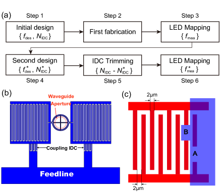
Step 1: Initial design of the MKID array. Assume we want to design an array of resonators with design frequencies of ( = 1, 2, .., ). The set usually forms a frequency comb which fits within a certain readout bandwidth. We can determine the desired number of IDC fingers of each resonator from the relation , where the total inductance and capacitance per finger are values derived from electro-magnetic simulations and material parameters obtained from previous experiments. In this initial design step, we have ignored any wafer non-uniformity and assumed common and among all the resonators.
Step 2: First fabrication. In this step, the wafer is patterned into an array of resonators with the design number of IDC fingers .
Step 3: Frequency measurement and LED mapping. It is straightforward to measure the transmission of the entire array which contains all the resonances using a vector network analyzer (VNA). However, it is difficult to correctly correspond each resonance to its physical resonator on the wafer because the resonances are shifted from their design values due to wafer non-uniformity. In this step, we use the LED wafer mapping tool that we have previously developed especially for this purpose LEDmapper to establish the correspondence between the measured frequency and the number of fingers of the -th resonator on the wafer.
Step 4: Array re-design. To account for the deviation of from due to wafer non-uniformity, we set up a new model , where and are introduced to account for the local variations of inductance and capacitance at the location of the -th resonator. By analyzing the vs. data obtained from Step 3, we retrieve the local product of each resonator. We then set up a new frequency comb as our new design frequencies. We require that , because in the next step we will etch off a small portion from the original IDC fingers. Calculated from using the derived values, the -th resonator is re-designed to have a new number of IDC fingers ().
Step 5: IDC trimming. In this step, the wafer is sent back to the clean room and a small portion of each IDC is trimmed off using lithographical tools and reactive ion etching which reduces the number of IDC fingers from to .
Step 6: Frequency re-measurement of the trimmed array. In this step, we repeat the VNA sweep and LED mapping procedures in Step 2 to obtain the new resonance frequencies . Comparison and statistics are carried out on both and to evaluate the effect of the array trimming technique.
To demonstrate our array trimming technique, we made a 127-pixel hexagonal close-packed LEKID array from a nm thick multilayer TiN/Ti/TiN film ( K) on a mm intrinsic Si wafer. Each pixel is identical to the BLAST-TNG pixel design Dober in the m band, which consists of orthogonal TiN absorbers attached to a pair of IDC (Fig. 1(b)). In this letter we study only the X-pol resonators.
In the initial design step (Step 1), the design resonance frequencies are in a geometric series as MHz , where = 1,…,127 is the resonator index along the meandering feedline on the wafer. The coupling quality factor is designed to be , which will yield a total quality factor under optical loading.
In the first fabrication step (Step 2), we patterned the wafer using a semi-automated “tiling and trimming” technique developed for BLAST-TNG arrays with a stepper tool McKenney . In this technique, a mask of the standard pixel tile (Fig. 1(b)) containing the common inductor part and an IDC with the maximum number of fingers, is repeatedly exposed onto the wafer at the desired pixel positions. A second set of IDC trimming masks (blue area in Fig. 1(c)) is used to cut each resonator’s IDC fingers at the desired position (position “A” in Fig. 1(c)) to create the designed frequency comb. This fabrication technique limits the number of stepper masks, ensures high quality and uniformity in the stepper lithography because all pixels are patterned from the same standard pixel mask, and provides considerable flexibility in resonator frequency definition and array layout.
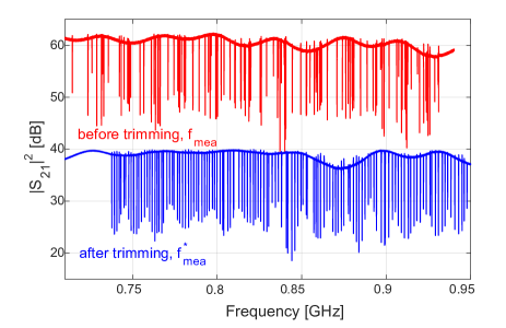
After the wafer is made, we cooled it down along with the LED-mapper setup in a dilution refrigerator. We measured the transmission of the MKID array at the base temperature of mK using a VNA and all the resonances were matched to their physical pixel on the wafer using the LED-mapper tool. As shown by the red curve in Fig. 2, 127 resonance dips are clearly observed in the frequency range spanned from MHz to MHz. Although the resonators are designed to have ideally spaced frequencies, some are too close and collide with their neighbors. If we use a 5-linewidth criterion for the frequency collision (the spacing between adjacent resonances is smaller than ), then resonances among the total resonances are in collision (taking ), resulting in a much reduced array yield of , despite the fabrication yield of .
In the re-design step (Step 4), in order to correct the effect of wafer non-uniformity, we selected a new set of design frequencies MHz and designed a new set of based on the local values obtained in Step 3.
In the next re-fabrication step (Step 5), the wafer was sent back to the clean room and a small portion of IDC finger () was lithographically patterned and removed for each resonator that requires frequency trimming (Fig. 1(c)). While it is possible to use the stepper tool and the same IDC trimming mask again to cut the IDC fingers, we used a maskless aligner (MLA) tool which is faster and more convenient. It directly exposes a pattern containing all areas to be etched off from a file onto the entire wafer without the need for a chrome mask. Although the lithography resolution of the MLA (1 micrometer) is poorer than the stepper (sub-micrometer), it is adequate for our purpose and the lithographical error has a negligible effect on the resonance frequency.
After IDC trimming, we measured the MKID wafer at mK again and the is shown by the blue curve in Fig. 2. One can see that the resonances are globally shifted up by about MHz since we have reduced the number of IDC fingers for most resonators. It is obvious that the uniformity of the frequency spacing after trimming is greatly improved. According to the 5-linewidth criterion of frequency collision, we find only colliding resonances out of a total of resonances, thus our technique has effectively improved the overall array yield from to .
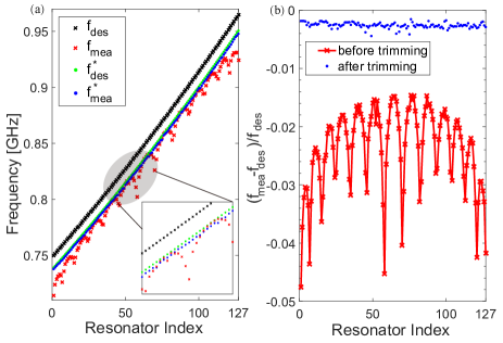
Fig. 3(a) shows the design and measured frequency before and after trimming. The fractional frequency deviation , which reveals the quantitative agreement between the measured and design frequencies, is plotted in Fig. 3(b). Before trimming, the exhibit an obvious periodic deviation from as shown in both Fig. 3(a) and (b). As discussed in our previous paper LEDmapper , this is caused by a radial non-uniformity of across the wafer in multilayer TiN/Ti/TiN films. Resonators near the turns of the meandering feedline are in general located on the outer ring of the wafer where the is lower and kinetic inductance is higher, leading to the larger negative deviation of the resonance frequency. On average, is lower by a factor of than its design value , which may be attributed to the inaccurate and values used in the initial design and the wafer non-uniformity. It is clear that the measured frequency is much closer to the design frequency after the trimming process, as shown in Fig. 3(b). The maximum deviation is only which is significantly smaller than that before trimming. We notice that all the measured frequencies shifted down by from the design frequencies. As a reference, the th resonator is untrimmed during the re-fabrication process () but its frequency also shifted down by like other trimmed resonators. This suggests that the global shift is a systematic effect (such as surface oxidation), which is not associated with the array trimming process.
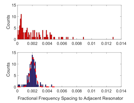
Fig. 4 compares the distribution of fractional frequency spacing for the MKID array before and after the trimming process. Here the fractional frequency spacing are calculated from . Before trimming, shows larger scatter from to while the design fractional spacing is . The scatter is greatly reduced after the trimming process. Taking , the 5-linewidth frequency collision criterion excludes (or ) resonators before trimming and only (or ) resonators after trimming. Therefore, the array yield is significantly improved.
The histogram in Fig. 4(b) fits well to a Gaussian distribution, which allows us to predict the ultimate array yield from the derived formula Supl
| (1) |
where is the probability for a resonator to survive collisions with all the other resonators, is the normalized resonator linewidth, is the designed fractional frequency spacing, and is the standard deviation of the Gaussian distribution. We set the number of linewidths to exclude to , which is the criterion used for frequency collision throughout this letter. As an example, the yield of a MKID array with resonators distributed in an octave bandwidth is predicted to be . This yield and the multiplexing density are desirable for many MKID instruments and their readout electronics.
Last, we have also verified that the quality factor and noise of the resonators remain unchanged before and after the trimming process. Therefore the detector performance is not affected.
In conclusion, we have demonstrated a wafer trimming technique which combines two successive rounds of design, fabrication and measurement together to produce a final resonator array with ideal frequency spacing and extremely low frequency collision rate. We use this technique on a 127-resonator array made from a TiN/Ti/TiN multilayer film and show that the array yield improves from to , while the resonator quality factors and noise properties remain unaffected. We have also demonstrated that the measured resonance frequency matches its design value within an accuracy of after the trimming process.
The proposed wafer trimming technique and its principle are applicable to any superconducting films, even films with poor wafer uniformity, and other resonator types than lumped-element resonators. It can also be easily modified to re-adjust other parameters of the array (such as the coupling ). Our technique provides an easy-to-implement and effective tool to improve the yield and multiplexing density of large resonator arrays, which may find broad applications in photon detection and quantum computing.
The MKID devices were fabricated in the NIST-Boulder microfabrication facility. We thank Prof. Xie Dong for his technical assistance. This work was supported in part by the National Natural Science Foundation of China (Grant Nos. 61301031, U1330201).
References
- (1) P. K. Day, H. G. LeDuc, B. A. Mazin, A. Vayonakis, and J. Zmuidzinas, Nature 425, 817 (2003).
- (2) M. A. Castellanos-Beltran, Kent D. Irwin, Leila R. Vale, Gene C. Hilton, and Konrad W. Lehnert, IEEE Trans. Appl. Supercond, 19, 944 (2009).
- (3) A. Blais, Ren-Shou Huang, A. Wallraff, S. M. Girvin, and R. J. Schoelkopf, Phys. Rev. A 69, 062320 (2004).
- (4) M. Will, M. Hamer, M, Muller, A. Noury, P. Weber, A. Bachtold, R. V. Gorbachev, C. Stampfer, and J. Guttinger, Nano Letter 17, 5950 (2017).
- (5) S. Doyle, P. Mauskopf, J. Naylon, A. Porch, and C. Duncombe, J. Low Temp. Phys. 151, 530 (2008).
- (6) J. Baselmans, J. Low Temp. Phys. 167, 292 (2012).
- (7) J. Zmuidzinas, Annual Review of Condensed Matter Physics 3, 169 (2012).
- (8) J. Baselmans, S. Yates, R. Barends, Y. Lankwarden, J. Gao, H. Hoevers, and T. Klapwijk, J. Low Temp. Phys. 151, 524 (2008).
- (9) J. Hubmayr, J. Beall, D. Becker, H.-M. Cho, M. Devlin, B. Dober, C. Groppi, G. C. Hilton, K. D. Irwin, D. Li et al, Appl. Phys. Lett. 106, 073505 (2015).
- (10) B. A. Mazin, B. Bumble, S. R. Meeker, K. O Brien, S. McHugh, and E. Langman, Optics Express 20, 1503 (2012).
- (11) D. Moore, S. Golwala, B. Bumble, B. Cornell, P. Day, H. LeDuc, and J. Zmuidzinas, Appl. Phys. Lett. 100, 232601 (2012).
- (12) S. Rowe, E. Pascale, S. Doyle, C. Dunscombe, P. Hargrave, A. Papageorgio, K. Wood, P. Ade, P. Barry, A. Bideaud et al, Rev. Sci. Instrum. 87, 033105 (2016).
- (13) J. Gao, M. Visser, M. Sandberg, F. Silva, S. Nam, D. Pappas, D. Wisbey, E. Langman, S. Meeker, B. Mazin et al, Appl. Phys. Lett. 101, 142602 (2012).
- (14) W. Guo, X. Liu, Y. Wang, Q. Wei, L. F. Wei, J. Hubmayr, J. Fowler, J. Ullom, L. Vale, M. R. Vissers et al, Appl. Phys. Lett. 110, 212601 (2017).
- (15) N. Galitzki, P. Ade, F. E. Angile, P. Ashton, J. Beall, D. Becker, K. J. Bradford, G. Che, H.-M. Cho, M. J. Devlin et al, J. Astron. Instrum. 3(02), 1440001 (2014).
- (16) A. Monfardini, L. Swenson, A.Bideaud, A. Cruciani, P. Camus, C. Hoffmann, F. Desert, S.Doyle, P. Ade, P. Mauskopf et al, Astrophys. J., Suppl. Ser. 194, 24 (2011).
- (17) J. Sayers, C. Bockstiegel, S. Brugger, N.G. Czakon, P.K. Day, T. P. Downes, R. P. Duan. J. Gao, A. K. Gill, et al, Proc. SPIE Int. Soc. Opt. Eng. 9153, 915304 (2014).
- (18) J. C. van Eyken, M. J. Strader, A. B. Walter, S. R. Meeker, P. Szypryt, C. Stoughton, K. OBrien, D. Marsden, N. K. Rice, Y. Lin et al, Astrophys. J., Suppl. Ser. 219, 14 (2015).
- (19) A. M. Baryshev, J. A. Baselmans, S. Yates, L. Ferrari, L. Bisigello, R. M.J. Janssen, A. Endo, T. M. Klapwijk, B. Klein, S. Heyminck and R. G sten, in Proc. Int. Conf. Infr., Millim., Terahertz Waves, (2014).
- (20) S. Shu, M. Calvo, S. Leclercq, J. Goupy, A. Monfardini, and E. Driessen, arXiv 1710, 08232 (2017).
- (21) M. Velázquez, D. Ferrusca, E. Castillo-Dominguez, E. Ibarra-Medel, S. Ventura, V. Gómez-Rivera, D. Hughes, I. Aretxaga, W. Grant, S. Doyle, and P. Mauskopf, J. Low Temp. Phys. 184, 799 (2016)
- (22) M. R. Vissers, J. Gao, J. S. Kline, M. Sandberg, M. Weides, D. S. Wisbey, and D. P. Pappas, Thin Solid Films, 548, 485-488 (2013).
- (23) M. R. Vissers, J. Gao, M. Sandberg, S. M. Duff, D. S. Wisbey, K. D. Irwin, and D. P. Pappas, Appl. Phys. Lett. 102, 232603 (2013).
- (24) B. A. Mazin, S. R. Meeker, M. J. Strader, P. Szypryt, D. Marsden, J. C. van Eyken, G. E. Duggan, A. B. Walter, G. Ulbricht, M. Johnson, et al, Publ. Astron. Soc. Pac. 125, 1348 (2013).
- (25) B. Dober, J. A. Austermann, J. A. Beall, D. Becker, G. Che, H. M. Cho, M. Devlin, S. M. Du, N. Galitzki, J. Gao et al, J. Low Temp. Phys. 184, 173 (2016).
- (26) X. Liu, W. Guo, Y. Wang, L. F. Wei, C. M. Mckenney, B. Dober, T. Billings, J. Hubmayr, L. S. Ferreira, M. R. Vissers, and J. Gao, 122, 034502 (2017).
- (27) C. M. McKenney, et al, in preparation.
- (28) See supplementary material for more details on resonator frequency collision and yield.