Equilibration of quantum hall edge states and its conductance fluctuations in graphene p-n junctions
Abstract
We report an observation of conductance fluctuations (CFs) in the bipolar regime of quantum hall (QH) plateaus in graphene (p-n-p/n-p-n) devices. The CFs in the bipolar regime are shown to decrease with increasing bias and temperature. At high temperature (above 7 K) the CFs vanishes completely and the flat quantized plateaus are recovered in the bipolar regime. The values of QH plateaus are in theoretical agreement based on full equilibration of chiral channels at the p-n junction. The amplitude of CFs for different filling factors follows a trend predicted by the random matrix theory. Although, there are mismatch in the values of CFs between the experiment and theory but at higher filling factors the experimental values become closer to the theoretical prediction. The suppression of CFs and its dependence has been understood in terms of time dependent disorders present at the p-n junctions.
I Introduction
Graphene, with unique linear dispersion, exhibits anomalous Quantum Hall effect (QHE) because the number of chiral edge modes at the boundary of a graphene flake increases by multiple of four plus twoZhang et al. (2005); Novoselov et al. (2005); Gusynin and Sharapov (2005); Neto et al. (2009). This results in half integer quantum Hall conductance plateaus as 4(n+1/2)/h with integer number nZhang et al. (2005); Novoselov et al. (2005); Gusynin and Sharapov (2005); Neto et al. (2009). Even though each Landau level (LL) has four degeneracy coming from two spins and two valleys (K and K′), the half or anomalous effect can be explained by taking into account that the valley degeneracy gets lifted at the boundary of the graphene flakeBrey and Fertig (2006). As a result for n = 0 LL there are only two chiral edge states coming from two spins degrees of freedom. The chiral edge states may not only occur at the boundary of a sample but can also form inside the sample. This can be realized by making a p-n junction in grapheneAbanin and Levitov (2007); Williams et al. (2007); Özyilmaz et al. (2007), where the four chiral states propagate along the junction preserving the valley degeneracy.
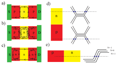
In recent years graphene p-n junction with perpendicular magnetic field has gained a lot of attention in condensed matter physicsWilliams and Marcus (2011); Schmidt et al. (2013); Amet et al. (2014); Rickhaus et al. (2015); Taychatanapat et al. (2015); Kumada et al. (2015); Matsuo et al. (2015); Morikawa et al. (2015); Klimov et al. (2015); Dubey and Deshmukh (2016); Fraessdorf et al. (2016). Such a p-n junction exhibits unprecedented phenomena like snake statesWilliams and Marcus (2011); Rickhaus et al. (2015); Taychatanapat et al. (2015), where the interface state in a semi-classical picture alternatively propagate in the p and n side of the junction. However, in a high magnetic field one needs to consider the quantum picture of the chiral states. Graphene flake with p-n junction has edge states’ at the boundary as well as the interface states’ at the junction. The conductance of such a p-n junction depends on how the electron coming from the source edge states enters into the interface states and flow out from the interface states to the counter propagating edge states This has been shown schematically in Figure 1 for a p-n junction having filling factor 2,-2 (Fig. 1a) and 6,-6 (Fig. 1b). Figure 1(c) and (d) shows the schematic of LL at the edge of graphene device and at the p-n junction interface respectively. The average conductance plateaus of such bipolar junctions (Fig. 1a and 1b) does not exhibit half integer values rather show fractional values as predicted by Abanin et.al Abanin and Levitov (2007), which depends on the equilibration of the interface states by disorders.
The theoretical prediction based on random matrix theory by Abanin et.al Abanin and Levitov (2007) and numerical simulations by J. Li et.al
Li and Shen (2008) predict that there will be large mesoscopic fluctuations in bipolar regime. Thus, for a given disorder configuration one can not observe the flat conductance plateaus. Theoretically, the flat conductance plateaus in bipolar regime were obtained by taking average over large number of disorder configurations or ensemble average. In an experiment, as there will be only one unique disorder configuration and thus, the CFs should emerge. For last one decade several experimentsWilliams et al. (2007); Özyilmaz et al. (2007); Liu et al. (2008); Lohmann et al. (2009); Velasco Jr et al. (2009); Ki and Lee (2009); Ki et al. (2010); Lohmann et al. (2009); Velasco Jr et al. (2010); Jing et al. (2010); Woszczyna et al. (2011); Nam et al. (2011); Velasco et al. (2012); Bhat et al. (2012); Schmidt et al. (2013); Amet et al. (2014); Klimov et al. (2015) have been performed on graphene p-n junction devices. Most of the experiments were carried out on Si substrate as global back gate and Al2O3/ HSQ/ PMMA/ air bridge as a local top gate. They have reported the observation of fractional conductance plateaus in bipolar regime. However, the inevitable CFs were not observed. The surprising results were explained by considering the time dependent fluctuations of disordersAbanin and Levitov (2007) at the p-n junction. As a consequence the system transforms into an ensemble average quantity and exhibits flat conductance plateaus. Abanin et.al Abanin and Levitov (2007) suggested that the suppression of CFs could be also explained by the de-phasing mechanism originating from the coupling between the localized states in the bulk with disorder state at the p-n junction.
In this paper we have carried out Quantum Hall measurements in hBN protected graphene devices. Our data for the first time reveals the evidence of CFs superimposed on QH plateaus in the bipolar region (p-n-p/n-p-n) of graphene. The CFs are shown to decrease with bias voltages as well as with temperature beyond a critical value. The CFs vanish completely at high temperature (7 K) and the exact value of the QH plateau was recovered (RefDubey and Deshmukh (2016)). However, there is a discrepancy between the amplitude of CFs of our experiment with the theoretical values (Abanin et al.Abanin and Levitov (2007)) at low filling factors. Interestingly, at higher filling factors the experimental values become very close to the theoretical prediction. In order to understand the suppression of CFs at lower filling factors we have also carried out noise measurement in the bipolar region. The above measurements suggest the existence of time dependent disorder in the devices.
II Device fabrication
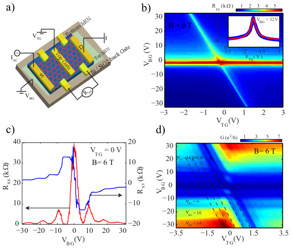
The schematic of the device is shown in figure 2(a). First a thin layer of hBN ( 20 nm) was transferred on a 300 nm thick Si , which was followed by transfer of a graphene using dry transfer technique Zomer et al. (2011). The contacts were fabricated using standard electron-beam lithography technique, followed by Cr/Au (5 nm/ 70 nm) deposition. The prepared heterostructure was vacuum annealed at 300∘C for 3 hours which was followed by a thin hBN ( 13 nm) transfer on the prepared Graphene-hBN-Si heterostructure. Finally, the top gate was defined using lithography, followed by Cr/Au (5nm/70 nm) deposition. The 300 nm thick Si serves as global back gate and thin top hBN ( 13 nm) as local top gate. Different combination of back and top gate voltages leads to the formation of unipolar (p-p-p/n-n-n) and bipolar (n-p-n/p-n-p) region. All the measurements were performed using standard lock-in technique at 6 T perpendicular magnetic field (except Fig. 2b) at a base temperature of 240 mk in a He3 refrigerator.
III Results and discussion
Figure 2(b) shows the 2D color plot of resistance as a function of back gate () and top gate () voltages at 240 mK at zero magnetic field. From the slope of diagonal line we calculate top hBN thickness to be 13 nm, which implies that the relative coupling of top gate with back gate is . The inset of Figure 2(b) shows the cut line at = 32 V. Red line is a fit to the curve with the following equationVenugopal et al. (2011):
| (1) |
where , , and are the contact resistance, mobility, length and width of top gate region, respectively. From the fitting we obtained a mobility of 25000 and contact resistance of 500 , with and .
III.1 Quantum hall plateaus in unipolar and bipolar regime
Figure 2(c) shows longitudinal resistance () and hall resistance () measured at 6 T perpendicular magnetic field at V. We see the clear LL plateaus at and the vanishing of components at the corresponding back gate voltages. The obtained QH resistance values are in exact agreement with the theoretical value for single layer graphene.
The resistance of a graphene device in high magnetic field depends on the filling factors , Williams et al. (2007); Özyilmaz et al. (2007); Abanin and Levitov (2007); Dubey and Deshmukh (2016). In the unipolar regime (with ) the QH edge states in the top gate region is fully transmitted as shown in Figure 1 (c) and the resistance is given asDubey and Deshmukh (2016)
is the two probe resistance measured between the source and drain (S and D of Fig. 2a). For the bipolar regime, the average value of the resistance depends on the equilibration of the interface states (Fig. 1a and 1b) and in the case of full mixing the resistance can be written asDubey and Deshmukh (2016)
Figure 2(d) shows the color plot of two probe conductance measured at
B = 6 T as a function of and . The horizontal strips and the dashed diagonal lines in Fig. 2d represents and , respectively. We observe clear QH plateaus for , in the unipolar regime.
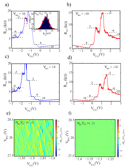
Figure 3(a), (b), (c) and (d) shows as a function of for = 10, -10, 14, -14, respectively. We obtain the expected quantized resistance values in the unipolar region. In the bipolar regime we observe the resistance fluctuation on top of the expected quantized quantum hall plateaus Abanin and Levitov (2007); Williams et al. (2007); Özyilmaz et al. (2007); Dubey and Deshmukh (2016). The dashed horizontal lines
in Fig. 3 (a), (b), (c) and (d) indicates the expected quantized resistance values in the unipolar and the bipolar regime. The similar CFs in the bipolar regime for has been shown in S.I.
In order to investigate the nature of CFs we have measured trans- resistance / as a function of and for plateau and is shown as 2D color plot in Fig. 3e. Figure 4 (c) shows the auto correlation of the data shown in Fig. 3e. It can be clearly seen from Fig. 3e and 4c that there is no clear pattern in the resistance fluctuations, thus, ruling out the possibility of any kind of Fabry-Perot interference, snake state, Aharonov Bohm interference or the oscillations arising from penetration of magnetic flux in the insulating area between the co-propagating p and n quantum Hall edge channelsMorikawa et al. (2015). The distribution of fluctuations show pure gaussian nature and has been shown in the inset of Fig. 3a. The histogram is extracted from the data shown in figure 3a, marked by dashed vertical red lines. Figure 3 (f) shows the 2D color plot of trans- resistance as a function of and for 14, 2 QH plateau (unipolar regime), indicating the absence of fluctuations in the unipolar regime.
III.2 Conductance fluctuation
The universal conductance fluctuation (UCF) is an ubiquitous quantum interference phenomena occurring in disordered mesoscopic devices at low temperatures. It has been a topic of great interest in graphene devicesSkákalová et al. (2009); Lee et al. (2012); Rahman et al. (2014a). As the coherent electron travel in all possible paths it get scattered repeatedly and the interference of these coherent waves give rise to UCF. When the phase coherence length is larger or comparable to the sample size, the conductance fluctuates with the universal magnitude of /h and is independent of the degree of disorder or the geometry of the device. It is predicted by Abanin et.al(Abanin and Levitov, 2007) that in a fully coherent regime conductance would exhibit UCF and the magnitude of UCF will depend on the number of channels as follows:
| (2) |
As mentioned earlier the resistance in our experiment was measured in a four-probe geometry. In order to compare with the theoretical predictions Abanin and Levitov (2007) we need to convert the resistance fluctuations into the conductance fluctuations. We have used the following method. The two probe conductance can be written as
where, and we have assumed that . Thus the maximum change in conductance can be written as
Hence, the standard deviation of conductance fluctuation can be written as
| (3) |
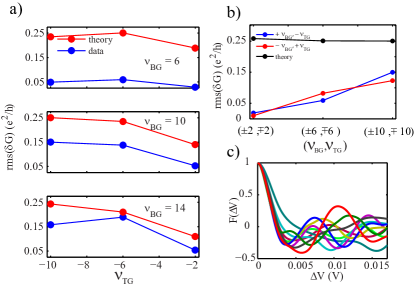
Figure 4(a) shows the magnitude of CFs as a function of , for different set of in the bipolar regime. We see that although the experimental and the theoretical values Abanin and Levitov (2007) have the same trend but there are large mismatch between the two values. Interestingly, with increasing , the discrepancy decreases and the values of experimental CFs approaches closer to the theoretical prediction. Figure 4(b) shows CFs as a function of and the values are same for p-n-p or n-p-n configuration. It is evident that with increasing filling factor, the mismatch between the measured CFs and the theoretical value decreases.
III.3 Dependence of conductance fluctuation on bias and temperature
Next we tune to = 10 and study the resistance fluctuation with bias and temperature.
Figure 5 (a) shows the resistance fluctuation as a function of at = 0 V and 1.6 mV. We notice that at = 1.6 mV the flat QH plateaus in the bipolar regime are almost recovered. Similarly, the resistance fluctuation was also killed with temperature. Figure 5b shows that at 9 K the fluctuation vanishes completely and we obtain the flat quantized plateaus in the bipolar regime.
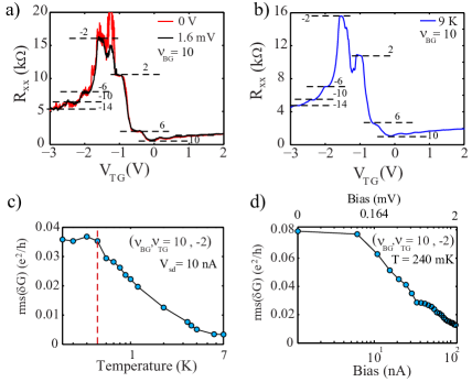
Figure 5c shows as a function of temperature for 10,-2 QH plateau. We see that fluctuation amplitude remains constant till 400 mK () and starts to decrease beyond this temperature. There were no detectable CFs beyond T = 7 K. Figure 5 (d) shows as a function of bias for 10,-2 QH plateau, obtained from figure 2 of S.I. It can be seen that remains constant till 6 nA which is equivalent to 130 eV () and decreases beyond this point. The complete suppression of conductance flutuation is seen mV. The complete suppression of CFs at temperature, T = 7 K or at bias, 2 mV are of similar energy scale(2 mV ). From fig. 5c (fig. 5d) it is clear that above () thermal energy is the main source of CFs suppresion. The energy scale can further be justified by comparing thermal length () versus the length of the p-n junction interface. The , where is the planks constant, is the Boltzman constant, T is the temperature and is the diffusion constant with a value of 250 ( see S.I). At T = 400 mK, , which is comparable to the length of the p-n junction of our device. Although the expression used for thermal length is valid at zero magnetic field, but we find it to be in good agreement with our data.
III.4 Conductance suppression mechanism
From Fig. 5c and 5d it is clear that above and the origin of CFs suppression is thermal energy broadening. However, the saturation value of CFs below and are far from the predicted theoretical valueAbanin and Levitov (2007). Abanin et. al has predicted the following origins as the source of CFs suppression:
(i) time dependent fluctuations of disorders at the p-n junction
(ii) some intrinsic de-phasing mechanism due to the coupling between localized states in the bulk with disorder states at the pn interface
A qualitative scheme to understand the suppression of CFs based on above origins has been depicted in Fig 6. It can be seen from Fig. 6a that the transmission at the p-n junction depends on how the discrete disorder energy levels are aligned with the Fermi energy position. Therefore, as a function of shifting, Fermi energy may align with one of the disorder levels or it may lie in between the disorder levels. For the case of alignment, half will be transmitted and half will be reflected back, in contrary everything will get reflected back for the non-alignment case, thus the CFs arises as a function of gate voltages or the Fermi energy shift. However, when the energy levels of the disorders are broadened (Fig. 6b), the transmission will relatively less sensitive on the location of the Fermi energy position, as a result the CFs will be suppressed. The origin of the broadening may arise due to above mentioned two mechanisms. The first origin coming from the time dependent disorder has been investigated by 1/f noise measurement.
The noise measurement is a versatile tool to capture the time dependent phenomena like traping-detraping of charges, disorder scattering, mobility fluctuation etc. There have been extensive studies of noise measurement in graphene devicesLin and Avouris (2008); Pal et al. (2011); Rahman et al. (2014b); Kumar et al. (2016). The schematic of noise measurement technique with experimental details and the defination of noise (A) has been mentioned in the S.I.
Figure 6c shows the noise power spectral density as a function of frequency in both unipolar (2,2; 6,6; 10,10) and bipolar regime (2,-2; 6,-6; 10,-10). It can be seen that in the unipolar regime the noise magnitude is very small and comparable to the background noise level (horizontal black solid line in Fig. 6c). This is indeed expected in the QH regime because the transprt through the chiral edge states are ballistic in nature. The detectable noise in the unipolar regime may arise from the contacts. However, in the bipolar regime transport occurs by tunneling between the LL via the defect states located at the p-n junction. Thus, one can expect to have noise coming from the time dependent fluctuation of disorders in the bipolar regime. It can indeed be seen from Fig.6c that in the bipolar regime the magnitude of noise is one order higher compared to unipolar regime.
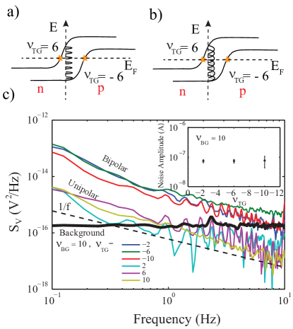
The inset of Fig. 6c shows the noise amplitude with filling factor in the bipolar regime. It is seen that the magnitude of noise in bipolar regime remains almost constant with increasing filling factor. This implies that the fluctuation of disorder levels does not change appreciably with increasing filling factor. Hence, increment in with increasing filling factor (Fig. 4a and 4b)can not be explained by the first origin. Thus, the time dependent fluctuation of disorder at the p-n junction is not sufficient enough to explain the suppresion of CFs. Hence we conjecture that the second dephasing mechanism is playing a significant role which can explain the increase in CFs with increasing filling factor. Further studies are required to understand the role of above mechanism in CFs suppression.
IV Conclusion
In conclusion we show first experimental signature of CFs in the bipolar regime in QH regime. The study also shows the crucial role of disorders in mixing the interface states at the p-n junction. By comparing the experimental values of CFs with the theoretical prediction as well as their dependence with increasing filling factors and noise measurements help us to separate out the contribution coming from the time dependent fluctuations of disorders at the p-n junction and de-phasing mechanism from the bulk. Our study will help in further understanding of edge state equilibration process at a p-n junction.
V Acknowledgements
We thank Tanmoy Das, Jeil Jung, Nicolas Leconte, Adhip Agrawal and Vijay Shenoy for helpful discussion. A.D. thanks nanomission under Department of Science and Technology, Government of India.
VI Appendix A. Supplementary data
Diffusion constant , 1/f noise measurement technique and experimental details, measurement performed on second device.
Supplementary Material: Equilibration of quantum hall edge states and its conductance fluctuations in graphene p-n junctions
Chandan Kumar1, Manabendra Kuiri1, and Anindya Das1
1Department of Physics, Indian Institute of Science, Bangalore 560012, India
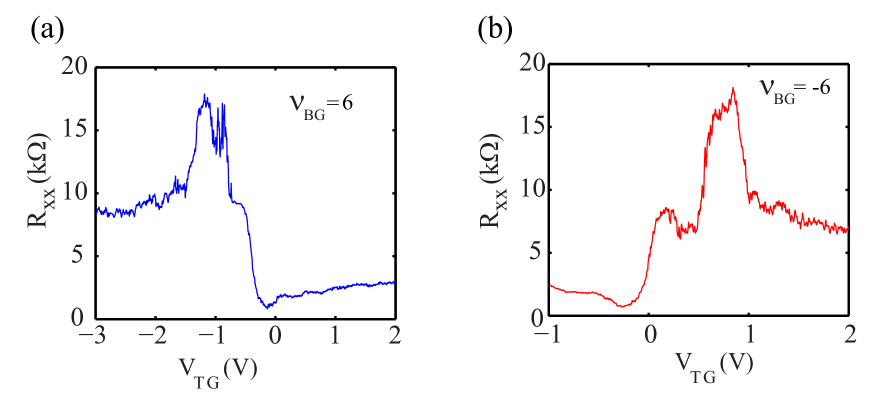
VII Conductance fluctuation in bipolar regime for different back gate filling factor
Figure 7(a)(b) shows as a function of for respectively. Clear fluctuation is visible in the bipolar regime on the quantum hall plateau while in the unipolar regime flat quantum hall plateau is obtained.
VIII Calculation of Diffusion constant
IX magneto resistance with bias
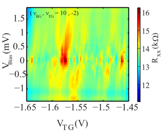
Figure 8 shows that the longitudinal resistance () as a function of bias for 10,-2 QH plateau. It can be clearly seen that the resistance fluctuation decreases with increasing bias voltage.
X noise measurement
Low frequency noise is a versatile tool to study charge dynamics,disorder scattering, statics of defects and dielectric screening. For various semiconductor, nano wire and graphene noise follows the Hooge’s emperical relationship:
where is the normalized voltage power spectral density,
is the frequency, is called Hooge parameter and is the total number of charge carriers. The exponent is ideally expected to be close to 1.
The noise amplitude (A) is defined as: .
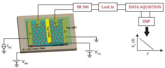
The noise measurement was done in He3 cryostat at a base temperature of 240 mK using ac lock in technique. The schematic of noise measurement technique is shown in figure 9. To measure noise, sample is biased with 25 nA current of frequency 228 Hz and the voltage fluctuation is measured with lock in amplifier using high speed 16 bit digital to analog converter (NI 6210 DAQ) card. The output voltage is amplified using SR 560 voltage amplifier before it is fed to the input of lock in amplifier (SR 830). The data is taken for 15 minutes with lock in time constant of 1 ms with roll off of 24dB/octave. The data is sampled at a rate of 32768 Hz and decimation factor was kept at 128 which gives the effective sampling rate of 256 Hz. The final step is DSP (digital signal processing). In this step the acquired data is anti-aliased, down sampled and Welch’s periodogram method is used for calulating PSD.
XI Measurement performed on second device
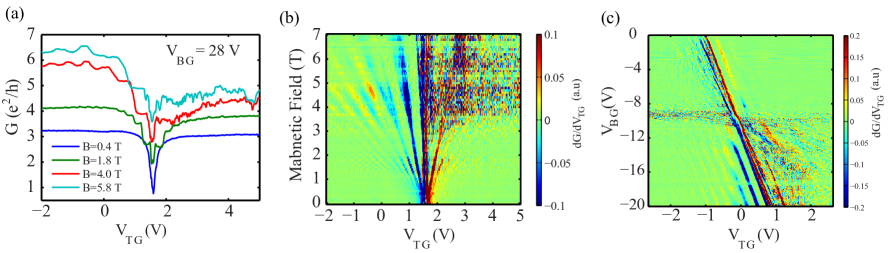
Figure 10 shows the result obtained on another single layer graphene device with top gate length of 1.25 , width of 2.1 and mobility of 9000 . Figure 10 (a) shows two probe conductance (in units if ) as a function of top gate voltage for different set of magnetic field at -28 V. Figure 10(b) shows transconductance as a function of magnetic field and top gate voltages for =-28 V. As can be seen from figure 10(a) and (b) at low magnetic field clear QH plaetau is seen in both unipolar and bipolar regime but as the field increases we start getting well quantized plateaus in unipolar regime but fluctuations in bipolar regime. Figure 10(c) shows transconductance as a function of and . In all of them (figure 4) we see clear Landau Level (LL) plateau in the unipolar region while in the bipolar regime we see fluctuation superimposed QH plateaus.
References
- Zhang et al. (2005) Y. Zhang, Y.-W. Tan, H. L. Stormer, and P. Kim, Nature 438, 201 (2005).
- Novoselov et al. (2005) K. Novoselov, A. K. Geim, S. Morozov, D. Jiang, M. Katsnelson, I. Grigorieva, S. Dubonos, and A. Firsov, nature 438, 197 (2005).
- Gusynin and Sharapov (2005) V. Gusynin and S. Sharapov, Physical Review Letters 95, 146801 (2005).
- Neto et al. (2009) A. C. Neto, F. Guinea, N. M. Peres, K. S. Novoselov, and A. K. Geim, Reviews of modern physics 81, 109 (2009).
- Brey and Fertig (2006) L. Brey and H. Fertig, Physical Review B 73, 195408 (2006).
- Abanin and Levitov (2007) D. Abanin and L. Levitov, Science 317, 641 (2007).
- Williams et al. (2007) J. Williams, L. DiCarlo, and C. Marcus, Science 317, 638 (2007).
- Özyilmaz et al. (2007) B. Özyilmaz, P. Jarillo-Herrero, D. Efetov, D. A. Abanin, L. S. Levitov, and P. Kim, Physical review letters 99, 166804 (2007).
- Williams and Marcus (2011) J. Williams and C. Marcus, Physical review letters 107, 046602 (2011).
- Schmidt et al. (2013) H. Schmidt, J. Rode, C. Belke, D. Smirnov, and R. Haug, Physical Review B 88, 075418 (2013).
- Amet et al. (2014) F. Amet, J. Williams, K. Watanabe, T. Taniguchi, and D. Goldhaber-Gordon, Physical review letters 112, 196601 (2014).
- Rickhaus et al. (2015) P. Rickhaus, P. Makk, M.-H. Liu, E. Tóvári, M. Weiss, R. Maurand, K. Richter, and C. Schönenberger, Nature communications 6 (2015).
- Taychatanapat et al. (2015) T. Taychatanapat, J. Y. Tan, Y. Yeo, K. Watanabe, T. Taniguchi, and B. Özyilmaz, Nature communications 6 (2015).
- Kumada et al. (2015) N. Kumada, F. Parmentier, H. Hibino, D. Glattli, and P. Roulleau, Nature communications 6 (2015).
- Matsuo et al. (2015) S. Matsuo, S. Takeshita, T. Tanaka, S. Nakaharai, K. Tsukagoshi, T. Moriyama, T. Ono, and K. Kobayashi, Nature communications 6 (2015).
- Morikawa et al. (2015) S. Morikawa, S. Masubuchi, R. Moriya, K. Watanabe, T. Taniguchi, and T. Machida, Applied Physics Letters 106, 183101 (2015).
- Klimov et al. (2015) N. N. Klimov, S. T. Le, J. Yan, P. Agnihotri, E. Comfort, J. U. Lee, D. B. Newell, and C. A. Richter, Physical Review B 92, 241301 (2015).
- Dubey and Deshmukh (2016) S. Dubey and M. M. Deshmukh, Solid State Communications 237, 59 (2016).
- Fraessdorf et al. (2016) C. Fraessdorf, L. Trifunovic, N. Bogdanoff, and P. W. Brouwer, arXiv preprint arXiv:1607.07758 (2016).
- Li and Shen (2008) J. Li and S.-Q. Shen, Physical Review B 78, 205308 (2008).
- Liu et al. (2008) G. Liu, J. Velasco Jr, W. Bao, and C. N. Lau, Applied Physics Letters 92, 203103 (2008).
- Lohmann et al. (2009) T. Lohmann, K. von Klitzing, and J. H. Smet, Nano letters 9, 1973 (2009).
- Velasco Jr et al. (2009) J. Velasco Jr, G. Liu, W. Bao, and C. N. Lau, New Journal of Physics 11, 095008 (2009).
- Ki and Lee (2009) D.-K. Ki and H.-J. Lee, Physical Review B 79, 195327 (2009).
- Ki et al. (2010) D.-K. Ki, S.-G. Nam, H.-J. Lee, and B. Özyilmaz, Physical Review B 81, 033301 (2010).
- Velasco Jr et al. (2010) J. Velasco Jr, G. Liu, L. Jing, P. Kratz, H. Zhang, W. Bao, M. Bockrath, C. N. Lau, et al., Physical Review B 81, 121407 (2010).
- Jing et al. (2010) L. Jing, J. Velasco Jr, P. Kratz, G. Liu, W. Bao, M. Bockrath, and C. N. Lau, Nano letters 10, 4000 (2010).
- Woszczyna et al. (2011) M. Woszczyna, M. Friedemann, T. Dziomba, T. Weimann, and F. J. Ahlers, Applied Physics Letters 99, 022112 (2011).
- Nam et al. (2011) S.-G. Nam, D.-K. Ki, J. W. Park, Y. Kim, J. S. Kim, and H.-J. Lee, Nanotechnology 22, 415203 (2011).
- Velasco et al. (2012) J. Velasco, Y. Lee, L. Jing, G. Liu, W. Bao, and C. Lau, Solid State Communications 152, 1301 (2012).
- Bhat et al. (2012) A. K. Bhat, V. Singh, S. Patil, and M. M. Deshmukh, Solid State Communications 152, 545 (2012).
- Zomer et al. (2011) P. Zomer, S. Dash, N. Tombros, and B. Van Wees, Applied Physics Letters 99, 232104 (2011).
- Venugopal et al. (2011) A. Venugopal, J. Chan, X. Li, C. W. Magnuson, W. P. Kirk, L. Colombo, R. S. Ruoff, and E. M. Vogel, Journal of Applied Physics 109, 104511 (2011).
- Skákalová et al. (2009) V. Skákalová, A. B. Kaiser, J. S. Yoo, D. Obergfell, and S. Roth, Physical Review B 80, 153404 (2009).
- Lee et al. (2012) D. S. Lee, V. Skákalová, R. T. Weitz, K. von Klitzing, and J. H. Smet, Physical Review Letters 109, 056602 (2012).
- Rahman et al. (2014a) A. Rahman, J. W. Guikema, and N. Markovic, PHYSICAL REVIEW B Phys Rev B 89, 235407 (2014a).
- Lin and Avouris (2008) Y.-M. Lin and P. Avouris, Nano letters 8, 2119 (2008).
- Pal et al. (2011) A. N. Pal, S. Ghatak, V. Kochat, E. Sneha, A. Sampathkumar, S. Raghavan, and A. Ghosh, ACS nano 5, 2075 (2011).
- Rahman et al. (2014b) A. Rahman, J. W. Guikema, and N. Marković, Nano letters 14, 6621 (2014b).
- Kumar et al. (2016) C. Kumar, M. Kuiri, J. Jung, T. Das, and A. Das, Nano letters 16, 1042 (2016).
- Bohra et al. (2012) G. Bohra, R. Somphonsane, N. Aoki, Y. Ochiai, R. Akis, D. Ferry, and J. Bird, Physical Review B 86, 161405 (2012).
- Mayorov et al. (2011) A. S. Mayorov, R. V. Gorbachev, S. V. Morozov, L. Britnell, R. Jalil, L. A. Ponomarenko, P. Blake, K. S. Novoselov, K. Watanabe, T. Taniguchi, et al., Nano letters 11, 2396 (2011).