Present address: ]Research Laboratory of Electronics, Massachusetts Institute of Technology, Cambridge, MA 02139, USA
Superconducting Gatemon Qubit based on a
Proximitized Two-Dimensional Electron Gas
The coherent tunnelling of Cooper pairs across Josephson junctions (JJs) generates a nonlinear inductance that is used extensively in quantum information processors based on superconducting circuits, from setting qubit transition frequencies koch_2007 and interqubit coupling strengths chen_2014 , to the gain of parametric amplifiers castellanos-beltran_2007 for quantum-limited readout. The inductance is either set by tailoring the metal-oxide dimensions of single JJs, or magnetically tuned by parallelizing multiple JJs in superconducting quantum interference devices (SQUIDs) with local current-biased flux lines. JJs based on superconductor-semiconductor hybrids represent a tantalizing all-electric alternative. The gatemon is a recently developed transmon variant which employs locally gated nanowire (NW) superconductor-semiconductor JJs for qubit control larsen_2015 ; delange_2015 . Here, we go beyond proof-of-concept and demonstrate that semiconducting channels etched from a wafer-scale two-dimensional electron gas (2DEG) are a suitable platform for building a scalable gatemon-based quantum computer. We show 2DEG gatemons meet the requirements divincenzo_2000 by performing voltage-controlled single qubit rotations and two-qubit swap operations. We measure qubit coherence times up to 2 s, limited by dielectric loss in the 2DEG host substrate.
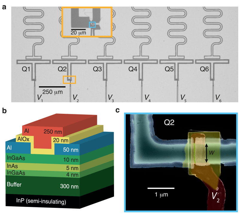
Figure 1(a) shows an optical micrograph of a typical device hosting six 2DEG gatemon qubits. Each gatemon comprises an Al island shunted to the ground plane via a 2DEG JJ and capacitively-coupled to a serpentine-shaped coplanar waveguide cavity. The self capacitance of the island together with the nonlinear inductance of the JJ creates an anharmonic potential for plasmon oscillations across the JJ. The ground and excited states of the qubit correspond to the lowest two harmonic oscillator states, which in the transmon limit () are separated in energy by a transition frequency , where is the charging energy, and is the Josephson energy koch_2007 ; clarke_2008 .
Fixed frequency transmons, employing single metal-oxide JJs, benefit from longer coherence times, but at the cost of slow ( 150 ns) two-qubit gate operation times sheldon_2016 and frequency crowding hutchings_2017 . Frequency tunable qubits allow faster two-qubit gates, but flux noise of 1 in SQUIDs limits phase coherence to 5 s kelly_2015 . Moreover, the milliampere currents used to control the flux in the SQUIDs place additional demands on cooling power and complicate the integration with 3D architectures. Qubit-qubit and qubit-coupler crosstalk can also exceed 4 and requires calibration protocols that scale with the number of qubits Neill_2017 . In superconductor-semiconductor JJs, can be controlled by local, capacitively-coupled gates delange_2015 ; larsen_2015 ; kjaergaard_2017 , opening up the possibility to tune and modulate without crosstalk or sensitivity to flux noise.
In this work we realize scalable superconductor-semiconductor JJs using the 2DEG heterostructure shown schematically in Fig. 1(b). The 2DEG is formed in an InAs quantum well encapsulated between InGaAs barriers. We leverage recent breakthroughs in in-situ epitaxy of Al on III-V semiconductors shabani_2016 to obtain a pristine high-transparency superconductor-semiconductor interface between a 50 nm-thick layer of superconducting aluminium and the 2DEG. Semi-insulating (Fe-doped) InP is used as a host substrate for the 2DEG buffer layer, which is etched away before patterning the qubit island and microwave control circuitry. Figure 1(c) shows a false coloured scanning electron micrograph of the JJ.
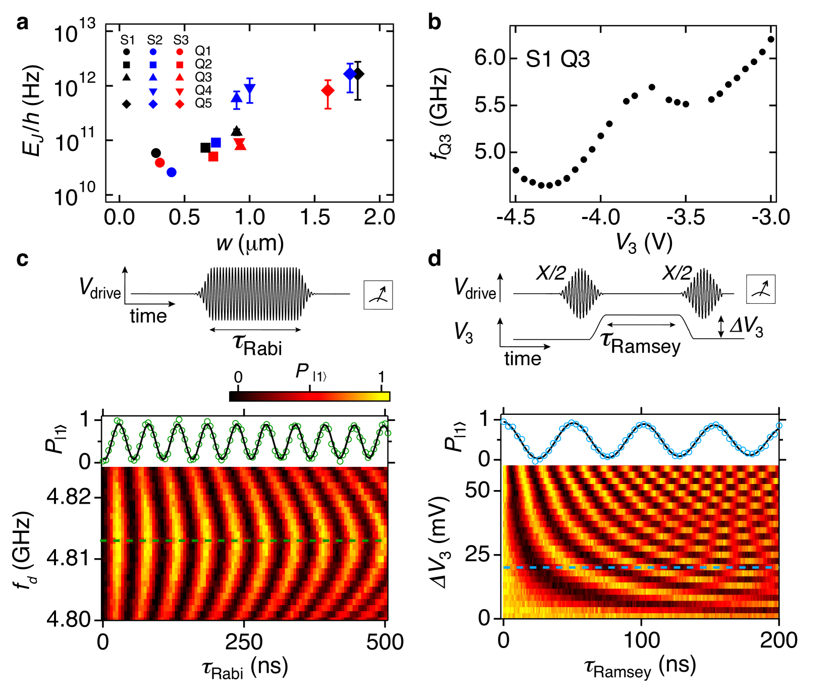
First, we demonstrate that 2DEG gatemons can be fabricated deterministically with reproducible properties. We fabricated three devices (S1, S2, S3) each hosting six qubits with junction width increasing from 0.3-2.6 m (labelled Q1-Q6). To extract of the as-fabricated qubits the corresponding cavity frequency is measured before any voltage is applied to the gate. Due to vacuum fluctuations in the electric field between the cavity and qubit, the cavity is Lamb-shifted from its bare resonance frequency by , where is the qubit-cavity detuning and is the coupling strength. This expression and the directly measured 100 MHz, together with numerical simulations for ( 230 MHz), allows us to estimate . Figure 2(a) plots the extracted as a function for all measured qubits. The data show that increases for wider junctions as expected for an increasing number of modes participating in Cooper pair transport kringhoj_2017 . Such precise control of on a design parameter represents an important step towards engineering scalable superconductor-semiconductor quantum information processors, improving on previous realizations where was limited by the 1D character of NWs.
Next, we show all-electric control by tuning the qubit transition frequency in Fig. 2(b). We operate in the transmon regime, 70-130, and read out the qubit dispersively () wallraff_2004 . Using two-tone spectroscopy, we drive a single qubit (Q3) and identify its frequency as a function of gate voltage from the state-dependent push on the cavity. The frequency is monotonic over a wider voltage range than for NWs larsen_2015 ; casparis_2016 and can be tuned by 1 GHz for 1 V applied to the gate (j corresponds to the voltage applied to j-th qubit Qj). The dependence of qubit frequency on gate voltage can be optimized by changing the thickness of the dielectric layer and using 2DEGs with different field-effect mobility.
We next demonstrate basic operations of individual qubits using time domain manipulation and readout. Phase-controlled microwave pulses with frequency are applied either via the cavity readout feedline or separately through the JJ top-gate. The rotation about the X-axis of the Bloch sphere is performed by applying the pulse for a time and reading out the state via the cavity [pulse sequence, Fig. 2(c)]. Plotting the probability to be in , , as a function of and , reveals Rabi oscillations [Fig. 2(c)], characteristic of the qubit rotation. These data are used to calibrate the pulse times and amplitudes to rotate by and around the X-axis ( and pulses respectively). We next show coherent accumulation of dynamical phase by controlled rotation of the qubit around the Z-axis. Fig. 2(d) shows the pulse sequence comprising a resonant () pulse, a gate pulse with amplitude and duration , and a second pulse. When = 0 the qubit and drive are phase locked, so the two pulses rotate the qubit to the state. With increasing the qubit rotates around the Z-axis relative to the drive. While further experiments are required to establish fidelities, these data establish the high degree of control afforded by electrostatically-coupled gates.
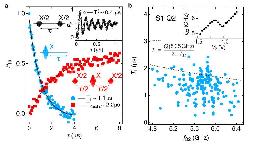
To measure the relaxation time, , an pulse excites the qubit [blue pulse sequence, Fig. 3(a)] and is plotted as a function of , the time delay before readout. The probability decreases exponentially due to relaxation. Fitting the decay (blue) yields 1.1 s. To extract the dephasing time , two slightly detuned pulses are applied, black pulse sequence Fig. 3(a) inset, separated by delay time . A fit to the decay of the resulting Ramsey fringes [inset Fig. 3(a)] gives a dephasing time 400 ns. In order to reduce inhomogeneous dephasing due to low-frequency noise, we perform a Hahn echo sequence comprising a refocusing pulse between two pulses [Fig. 3(a), red]. The extracted 2.2 s indicates that 2DEG gatemon dephasing is dominated by low frequency noise bylander_2011 . Figure 3(b) shows as a function of qubit frequency. Relaxation times vary between 0.2 - 2 s and fluctuate strongly with [the spectrum is plotted in the inset Fig. 3(b)]. Owing to their periodicity, we attribute these fluctuations to on-chip modes, which is consistent with previous results from devices lacking crossover wire bonds.
An estimate for the dielectric loss of the qubit capacitor can be made using a test resonator coupled to the same feedline ( = 5.35 GHz) which shows an internal quality factor at low photon number. Using the expression we expect the relaxation time due to dielectric loss to follow the black dashed line barends_2013 . The agreement between the measured times and this upper bound suggests the qubit lifetime is indeed limited by dielectric loss. Similar ’s are obtained on pure semi-insulating InP substrates, suggesting the presence of the 2DEG does not introduce additional loss. Potential solutions for reducing microwave loss in InP include deep-etching bruno_2015 and using flip-chip techniques to host the qubit island on a low-loss substrate such as Si rosenberg_2017 . Using the measured lever arm of 1 GHz/V and gate voltage fluctuations of 8 V measured in III-V semiconductors dial_2013 , we expect an upper limit of 20 s, suggesting the prospects are good for obtaining coherence times comparable with state-of-the-art flux-tuneable transmons, where 30 s and 5 s kelly_2015 .
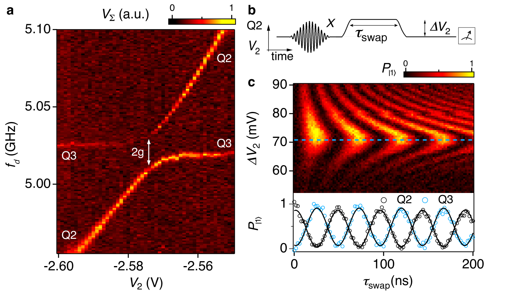
Finally, we coherently swap excitations using the capacitive coupling between neighbouring qubits. The monotonicity and reproducibility of the qubit spectra established in Fig. 2 are critical for tuning adjacent qubits into resonance with each other. The signature of qubit-qubit coupling is a mutual push on the bare qubit frequencies due to hybridization. To detect this push, the qubits Q2 and Q3 are driven and read out through the feedline and their respective cavities. For clarity the signals detected from both cavities are added to yield the sum . Figure 4(a) shows as a function of the qubit drive and . As expected, due to the absence of cross-talk, there are two peaks in as a function of , only one of which (Q2) is tuned by . When tuned onto resonance, the qubits anticross and a splitting of 12 MHz between the two hybridized states is observed, where is the qubit-qubit coupling strength. Figure 4(b) shows the pulse sequence that exploits the anticrossing to coherently transfer an excitation between Q2 and Q3, the starting point for preparing arbitrary two-qubit states. With the two qubits detuned by 140 MHz and Q3 idling, Q2 is prepared in . A gate pulse is then applied for time and brings Q2 into resonance with Q3 majer_2007 . Note that here the microwave pulses are applied through the gate line, demonstrating qubit manipulation using a single control line per qubit. We emphasize that single-gate control of rotations around the X, Y and Z-axis is an important advantage of voltage-controlled qubits. The rate at which excitations swap between qubits depends on and the pulse amplitude . Figure 4(c) shows the typical chevron pattern of swap oscillations hofheinz_2009 . The lower inset in Fig. 4(c) shows for each qubit separately. The anticorrelation confirms that the excitation is transferring between Q2 and Q3 and demonstrates the possibility of generating entangled states using 2DEG gatemon qubits. From sinusoidal fits (solid lines) an interaction rate 14 MHz is extracted, in good agreement with electrostatic simulations yielding 15 MHz for 5 GHz.
In summary, we have demonstrated that planar semiconductor materials and superconducting microwave circuits are compatible technologies that can be readily integrated while maintaining quantum coherence. This opens new possibilities for highly integrated quantum processors with on-chip components. Through a combination of geometry and applied voltages, can be tailored to simultaneously suit qubits as well as peripheral control circuits requiring higher , such as tuneable couplers chen_2014 ; casparis_2018 and on-chip microwave sources cassidy_2017 , and develop naturally into 3D architectures required to implement fault-tolerant processing versluis_2016 ; rosenberg_2017 . Moreover since 2DEG gatemons represent a perfect quantum counterpart to semiconductor-based cryogenic classical control logic ward_2013 ; al-taie_2013 ; hornibrook_2014 , they take the first step towards realizing a scalable all-electric hybrid superconductor-semiconductor quantum processor.
I Methods
I.1 The sample
Separate transport characterization shows that the 2DEGs exhibit a Hall mobility of approximately 2000 cm2V-1s-1 and an induced gap of 200 . The qubits were fabricated by first wet etching a mesa for the qubit JJ. The width of the JJ was defined by the mesa etch. The JJ was then formed by selectively wet etching a 100 nm long segment of the 50 nm thick Al. A 20 nm thick AlOx layer (yellow in Fig. 1(b)-(c)) was deposited as a gate dielectric, followed by the evaporation of an Al top gate (red). The heterostructure and the buffer were removed almost everywhere on the chip, leaving only a few micron large mesa region to form the active region of the qubit. The qubit islands, gate lines and readout cavities were defined in a lift-off process with a 100 nm Al layer. Finally, the epitaxial Al layer on top of the mesa and the microwave circuit were connected in a contact step. For each qubit, is determined by the capacitance of the T-shaped Al island to the surrounding ground plane and designed to be 230 MHz. All qubits are coupled to individual /4 superconducting cavities with resonant frequencies separated by 50 MHz and centred around 7.25 GHz. All six cavities are coupled to a common feed line barends_2013 .
I.2 Qubit manipulation and readout
All measurements presented in the paper are performed in a cryogen-free dilution refrigerator with a base temperature below 50 mK. The sample is mounted inside an Al box to suppress magnetic fluctuations. This box is placed inside a Cu box used to mount the sample at the mixing chamber plate of the refrigerator. Both boxes are closed but not light tight and are further surrounded by a cylindrical cryoperm shield, which is also thermally anchored to the mixing chamber.
The qubit is initialized in the state by waiting for much longer than the relaxation time . To manipulate a single qubit, one coaxial line and a DC line are used: the coax line is filtered by a Minicircuits VLF-320 low pass filter and an ECCOSORB filter to reduce noise while allowing for gate pulses. At high frequencies (2 GHz), the filter attenuates by roughly 20 dB allowing to drive the qubit directly. The DC line is filtered with an RC filter and added with a bias T at low temperature. For X microwave control as well as readout, the pulses are shaped through IQ modulation of the microwave source and using an AWG channel for I and Q respectively. For readout, the signal line is heavily attenuated (60 dB) to reduce both the thermal occupation of the resonator and noise to the sample. After passing through a magnetically shielded isolator, a travelling wave parametric amplifier macklin_2015 , another magnetically shielded isolator, a cryogenic low noise factory HEMT amplifier and another amplification stage at room temperature the qubit readout signals are mixed down to intermediate frequencies with a local oscillator, before sampling and performing digital homodyne detection to extract the cavity magnitude response. Qubit state measurements are obtained by averaging over 1000 experimental runs. We use the raw Rabi oscillation data for qubit state assignments. The data in Fig. 2(a) were acquired with a vector network analyzer. The data in all other figures were acquired using heterodyne detection in the dispersive regime. For Fig. 4 we combine two drives with frequencies close to the resonance frequencies of the cavities of Q2 and Q3 on the signal line.
Acknowledgements.
II Acknowledgments
We acknowledge helpful discussions with A. C. C. Drachmann, H. J. Suominen, E. O’Farrell, A. Fornieri, A. Whiticar and F. Nichele. This work was supported by Microsoft Project Q, the U.S. Army Research Office, the Innovation Fund Denmark, and the Danish National Research Foundation. C.M.M. acknowledges support from the Villum Foundation. MRC was supported by a Marie Curie Fellowship and EPSRC (EP/L020963/1). MK gratefully acknowledges support from the Carlsberg Foundation. The travelling wave parametric amplifier used in this experiment was provided by MIT Lincoln Laboratory and Irfan Siddiqi Quantum Consulting (ISQC), LLC via sponsorship from the US Government.
III Author contributions
T.W., C.T., S.G., G.C.G. and M.J.M. grew the proximitized 2DEG. M.K., L.C., C.M.M. and K.D.P designed the experiment. L.C., M.R.C., A.K., N.J.P., T.W.L., and K.D.P. prepared the experimental setup. L.C. and M.R.C. fabricated the devices and performed the experiment. L.C., M.R.C., M.K., A.K., T.W.L., F.K., C.M.M., and K.D.P. analyzed the data and prepared the manuscript.
IV Competing financial interest
The authors declare no competing financial interests.
References
- (1) Koch, J. et al. Charge-insensitive qubit design derived from the Cooper pair box. Phys. Rev. A 76, 042319 (2007).
- (2) Chen, Y. et al. Qubit Architecture with High Coherence and Fast Tunable Coupling. Phys. Rev. Lett. 113, 220502 (2014).
- (3) Castellanos-Beltran, M. A. & Lehnert, K. W. Widely tunable parametric amplifier based on a superconducting quantum interference device array resonator. Appl. Phys. Lett. 91, 083509 (2007).
- (4) Larsen, T. W. et al. A semiconductor nanowire-based superconducting qubit. Phys. Rev. Lett. 115, 127001 (2015).
- (5) de Lange, G. et al. Realization of microwave quantum circuits using hybrid superconducting-semiconducting nanowire josephson elements. Phys. Rev. Lett. 115, 127002 (2015).
- (6) Vincenzo, D. The physical implemenation of quantum computation. arXiv preprint, arXiv:quant-ph/0002077 (2000).
- (7) Clarke, J. & Wilhelm, F. K. Superconducting quantum bits. Nature 453, 1031–1042 (2008).
- (8) Sheldon, S., Magesan, E., Chow, J. M. & Gambetta, J. M. Procedure for systematically tuning up cross-talk in the cross-resonance gate. Phys. Rev. A 93, 060302 (2016).
- (9) Hutchings, M. D. et al. Tunable Superconducting Qubits with Flux-Independent Coherence. arXiv preprint arXiv:1702.02253 (2017).
- (10) Kelly, J. et al. State preservation by repetitive error detection in a superconducting quantum circuit. Nature 519, 66–69 (2015).
- (11) Neill, C. et al. A blueprint for demonstrating quantum supremacy with superconducting qubits. arXiv preprint arXiv:1709.06678 (2017).
- (12) Kjaergaard, M. et al. Transparent Semiconductor-Superconductor Interface and Induced Gap in an Epitaxial Heterostructure Josephson Junction. Phys. Rev. Applied 7, 034029 (2017).
- (13) Shabani, J. et al. Two-dimensional epitaxial superconductor-semiconductor heterostructures: A platform for topological superconducting networks. Phys. Rev. B 93, 155402 (2016).
- (14) Kringhøj, A. et al. Anharmonicity of a Gatemon Qubit with a Few-Mode Josephson Junction. arXiv preprint arXiv:1703.05643 (2017).
- (15) Wallraff, A. et al. Strong coupling of a single photon to a superconducting qubit using circuit quantum electrodynamics. Nature 431, 162–167 (2004).
- (16) Casparis, L. et al. Gatemon Benchmarking and Two-Qubit Operations. Phys. Rev. Lett. 116, 150505 (2016).
- (17) Bylander, J. et al. Noise spectroscopy through dynamical decoupling with a superconducting flux qubit. Nat. Phys. 7, 565–570 (2011).
- (18) Barends, R. et al. Coherent Josephson Qubit Suitable for Scalable Quantum Integrated Circuits. Phys. Rev. Lett. 111 (2013).
- (19) Bruno, A. et al. Reducing intrinsic loss in superconducting resonators by surface treatment and deep etching of silicon substrates. Appl. Phys. Lett. 106, 182601 (2015).
- (20) Rosenberg, D. et al. 3d integrated superconducting qubits. npj Quantum Information 3 (2017).
- (21) Dial, O. E. et al. Charge Noise Spectroscopy Using Coherent Exchange Oscillations in a Singlet-Triplet Qubit. Phys. Rev. Lett. 110, 146804 (2013).
- (22) Majer, J. et al. Coupling superconducting qubits via a cavity bus. Nature 449, 443–447 (2007).
- (23) Hofheinz, M. et al. Synthesizing arbitrary quantum states in a superconducting resonator. Nature 459, 546–549 (2009).
- (24) Casparis, L. et al. A voltage-controlled superconducting quantum bus. in preparation (2017).
- (25) Cassidy, M. C. et al. Demonstration of an ac Josephson junction laser. Science 355, 939–942 (2017).
- (26) Versluis, R. et al. Scalable quantum circuit and control for a superconducting surface code. Phys. Rev. Applied 8, 034021 (2017).
- (27) Ward, D. R., Savage, D. E., Lagally, M. G., Coppersmith, S. N. & Eriksson, M. A. Integration of on-chip field-effect transistor switches with dopantless Si/SiGe quantum dots for high-throughput testing. Appl. Phys. Lett. 102, 213107 (2013).
- (28) Al-Taie, H. et al. Cryogenic on-chip multiplexer for the study of quantum transport in 256 split-gate devices. Appl. Phys. Lett. 102, 243102 (2013).
- (29) Hornibrook, J. M. et al. Cryogenic Control Architecture for Large-Scale Quantum Computing. Phys. Rev. Applied 3, 024010 (2015).
- (30) Macklin, C. et al. A near–quantum-limited Josephson traveling-wave parametric amplifier. Science 350, 307–310 (2015).