A Compact CMOS Memristor Emulator Circuit and its Applications
Abstract
Conceptual memristors have recently gathered wider interest due to their diverse application in non-von Neumann computing, machine learning, neuromorphic computing, and chaotic circuits. We introduce a compact CMOS circuit that emulates idealized memristor characteristics and can bridge the gap between concepts to chip-scale realization by transcending device challenges. The CMOS memristor circuit embodies a two-terminal variable resistor whose resistance is controlled by the voltage applied across its terminals. The memristor ’state’ is held in a capacitor that controls the resistor value. This work presents the design and simulation of the memristor emulation circuit, and applies it to a memcomputing application of maze solving using analog parallelism. Furthermore, the memristor emulator circuit can be designed and fabricated using standard commercial CMOS technologies and opens doors to interesting applications in neuromorphic and machine learning circuits.
Index Terms:
Memristors, memcomputing, neuromorphic, non-von Neumann computing, ReRAM.I Introduction
Moore’s Law has enabled the semiconductor industry to sustain continual advancement in computing architectures by steadily scaling transistor size, and adding more architectural complexity while improving the energy-efficiency of the integrated circuit architectures. This has sustained the development of several key computing and communication technologies for several decades. However it appears that in order to continue gaining from the transistor bounty of Moore’s scaling in the nanometer regime, we need to radically rethink existing computing architectures. The new architectures are required to transcend the device variability and interconnect scaling bottlenecks of the traditional von-Neumann architecture, should exploit massive parallelism and locally employ memory within the computing elements in a manner similar to biological brains. One emerging technology that is promising for such computing architectures is memristors, or resistive RAM (ReRAM). Recent progress in memristive devices has spurred renewed interest in reconfigurable and neuromorphic computing architectures [1, 2, 3, 4, 5].
The memristive devices, integrated with conventional CMOS, are expected to realize low-power neuromorphic circuits with increased reconfigurability and smaller physical layout area [6, 7]. Since multi-valued memristor device technology is yet to mature and its analog behavior in-situ with circuits is still being characterized in the literature[8, 9, 10], we propose a low-risk and robust alternative for prototyping machine learning and neuromorphic systems in standard CMOS. The rest of the manuscript is organized as follows. Section II presents a brief background on memristors along with the defining characteristics of memristive circuits and devices. Section III presents the CMOS memristor (emulator) circuit along with simulation results. Finally Section IV presents an application using the proposed circuit, followed by conclusion.
II Memristor Characteristics
Memristor was defined as a two-terminal circuit-theoretic concept in a seminal paper by Chua [11], and later extended to a wider class of memristive systems [12]. The generic equation to describe such memristive systems is given by
| (1) |
| (2) |
where represents the state, and are the outputs of the system respectively, is a continuous function n-valued function, and is a scalar function [13, 3]. This relation can be interpreted as a voltage-controlled memristor, where the current () in the memristor is related to the voltage () by
| (3) |
with its state update equation
| (4) |
Here, is called memductance (i.e. memory conductance), and depends upon the charge that has flown across the device [3]. Decades later in year 2008, HP correlated the ideal memristor concept with a metal-oxide resistive switching thin-flim device [1]. In the same paper, a linear ion drift model was introduced to describe the behavior of the memristive device. Since then, several models have been investigated to fit the equations to the experimental device behavior [14, 15, 3]. A unique set of ‘fingerprints’ have been established based on the underlying circuit theory, to distinguish memristors from other resistance-switching devices. A memristor must exhibit a ‘pinched’ hysteresis loop that must pass through the origin in its switching curve, when the applied sinusoid input is zero [16]. Further, the pinched hysteresis loops of ideal memristors must be odd symmetric, otherwise they are modeled as generic memristive devices [16]. Another fingerprint of a memristor is that, as the frequency of the input sinusoid is increased, the area enclosed in the pinched loops progressively shrinks and eventually collapses to a straight line, or a single-valued function [3]. The fundamental promise of the memristors lies in the ‘analog’ memory, that endows it with the ability to store as well as manipulate information in analog-domain, opposed to digital very large-scale integrated circuits (VLSICs). Furthermore, these elements can be combined to realize analog computing parallelism, enshrined under memcomputing [17, 3, 18]. This analog computing ability is also harnessed in neuromorphic computing, where memristors realize analog synapses that learn based on spike-timing dependent plasticity (STDP), a local computing rule that is being investigated as an unsupervised learning approach for deep learning [6, 19, 20, 8, 21, 10].
III CMOS Memristor Emulator Circuit
In-spite of several promising features of idealized memristors, their large-scale adoption has been impeded by the practical limitations of fabricated memristive or resistive-RAM (ReRAM) devices. Device characteristics such as the switching threshold voltages and resistances are variable (and stochastic) for each device and across several devices, and depend upon the initial ‘forming’ step [22, 23, 24]. Further, it is challenging to realize stable weights for more than 1-bit resolution in filamentary devices due to the relaxation of the filament and is currently being addressed in device research [25, 10]. HfOx and TaOx based devices have exhibited up to 9 states and their performance within a circuit is being investigated [26]. A greater impediment from circuit design perspective is the lower on-resistance observed in reported devices (), which leads to power hungry driver circuits, and thus a fundamental trade-off between parallelism and energy-efficiency. Moreover, memristive devices fall well short of CMOS components in terms of their endurance. Thus, it is desirable to realize CMOS memristor (emulator) circuits for system-level design memcomputing exploration while the memristive devices mature and are integrated into a commercially available CMOS platform.

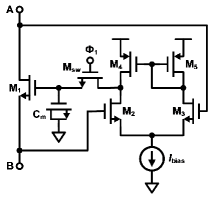
We disclosed the dynamic memristor/synapse circuit concept in the patent application [27]. In this work, we present CMOS memristor circuit design details, analysis, and its application in memcomputing. The fundamental concept is illustrated in Fig. 1 (a), where an n-channel MOSFET (NMOS) implements a floating variable resistance between terminals A and B. The variable resistance is achieved by operating the transistor in linear (triode) or near-linear region. The voltage difference across the terminals A and B, , is sensed, integrated over time and then used to control the gate of the transistor . The integrator holds the ‘state’ of the variable resistor and updates it according to the voltage difference . If a positive voltage is applied across the resistor, the gate voltage is increased and thus resulting in a decrease in the resistance (or an increase in conductance) across A and B. Similarly, a negative potential across the resistor results in an increase in the resistance (or decrease in conductance). This circuit embodying a variable resistor with a dynamic memory, realizes the functionality of the idealized memristor concept. Further, this compact circuit can be modified to implement analog synapses that exhibits bio-compatible learning rules, including the spike-timing dependent plasticity (STDP) [27].
| Device | Type | Sizing (W/L) or value |
|---|---|---|
| ZVT NMOS | ||
| NMOSCAP | , | |
| NMOS | ||
| NMOS | ||
| PMOS | ||
| PMOS | ||
| NMOS | ||
Fig. 1(b) shows one of several possible circuit implementations of a voltage-controlled memristor, and its transistor-level implementation is shown in Fig. 2. The circuit was implemented in a 130-nm CMOS process with a supply voltage of , and the extracted layout was simulated in Cadence Spectre. The corresponding device sizes are listed in Table I. Here, the transconductor senses the voltage across the two terminals, produces a small-signal current which is integrated into the charge stored on capacitor , with an effective gain . The current integration phase can be controlled by an external strobe or clock signal , whose utility will be apparent later in this section. When is , the capacitor is disconnected from the transconductor and holds the stored charge; thus realizing a dynamic analog memory. The value of can be in the range of - in CMOS implementation, and the ratio determines the pinched hysteresis characteristics (i.e. the width of the lobes) for a given input frequency, . Here, the voltage across the capacitor, , controls the gate of and referred to as the ‘state’ of the synapse. Assuming that the transistor is in deep-triode, the current flowing through the synapse is given by
| (5) |
where and are the gate-to-source and threshold voltages, and is the transconductance parameter, is the width and is the length of the NMOS . If the source of is held at a common-mode voltage , the above equation can be equivalently interpreted as the variable conductance ()
| (6) |
which expresses a direct relation between the state () and the conductance (). In order to force in triode for large drain-source voltage swings, a zero-threshold voltage transistor (ZVT) device () available in standard CMOS platforms is preferred. Also, in these scaled CMOS technologies, the MOSFET output resistance () in moderate saturation is inherently low due to short channel effects. This allows the proposed circuit to exhibit desired memristive behavior even when is in moderate saturation. In general, the dynamics of the memristor emulator circuit can be described as
| (7) |
| (8) |
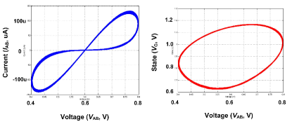
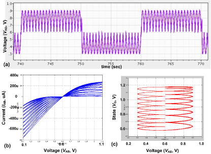
The simulated current-voltage hysteresis curve for the memristor circuit is shown in Fig. 3. The memristor was swept with a sinusoidal input of frequency 1 MHz, amplitude 200mV and a common-mode DC offset equal to 600mV, while was held at logic high (1.2 V). The circuit characteristics in Fig. 3(a) exhibit a pinched hysteresis curve typical of an ideal memristor. The memory effect in the synapse is further confirmed by the elliptical-like state trajectory seen in Fig. 3(b). The memristor circuit is further characterized by applying a modulated half sine-wave (derived from a sine-wave of 1 GHz frequency) as shown in Fig. 4(a). This waveform can be understood as successive voltage sweeps being applied to the synapse, to trace closely spaced analog memory states. The circuit characteristics in Fig. 4(a) further exhibit near-ideal memristor behavior with multiple pinched lobes. The synapse state trajectory seen in Fig. 4(b), which demonstrates that the synapse can hold fine-grained analog memory states that can be precisely controlled by an external stimulus. Moreover, the pinched lobes collapse into a straight line as the input frequency is increased, as a signature of memristors as discussed in Section II. An advantage of this circuit is that the resistance range of the emulated memristor can be chosen as desired depending upon the sizing of NMOS ; a flexibility not conveniently available with memristive devices.
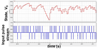
The memristor circuit in Fig. 2 inherently realizes a current-mode sample-and-hold to hold the analog state of the synapses. The sampling switch () prevents the transconductor ’s output from leaking the state ) on capacitor when no inputs are applied (since ’s output impedance is finite). This operation can also be interpreted as an energy barrier which prevents the stored electrons on from leaking-out immediately. The electrons will however leak-out eventually due to subthrehsold and junction leakages in the MOSFETs. However, we can achieve storage times of up to several seconds by using large and a low-leakage devices. Fig. 2 shows transient simulation results which exhibit the analog state manipulation and short-term retention property of the dynamic memristor. Here, a pseudo-random sequence is applied with ( =5 ns, amplitude, DC offset) and 1 MHz clock rate. We can observe that the state, , is incrementally updated corresponding to a positive or negative pulse input. Since the conductance updates of the memristor are monotonic with respect to the applied pulses (or voltage spikes), it can be used to dynamically store analog weights in a machine learning or spiking neural network circuit [8]. The drain-source resistance of is altered by updating the gate voltage, , by applying spikes across the terminals A-B. Assuming, rectangular spiking pulses, the incremental update in the gate voltage can be expressed as
| (9) |
where and are the spike height and width respectively.
The presented memristor circuit was conceived while trying to understand the relation between the pinched hysteresis behavior of memristor and their ability to hold analog states. As shown in this work, the switch is not needed for generating the pinched hysteresis sweep, but is essential for retaining the analog state by presenting a barrier for the charge to leak away. This reinforces the understanding that in order to realize analog memristive device, an electrochemical, tunneling[28] or other form of barrier is needed to retain multiple analog-like states. Also, in the presented dynamic memristor, the state eventually leaks away. A bistable version of the circuit can be realized by incorporating a weak latch structure to quantize the dynamic state for long-term binary retention (see [27]).
The transconductor-based memristor emulator circuit presented in this work, even though simple in structure, offers tremendous advantages over previously reported emulators [29]. The circuit is compact, consumes very small bias current (), can be fabricated in standard CMOS technology, offers design flexibility to choose memristor specifications, and doesn’t require an analog-to-digital converter (ADC)[30], or opamps [31, 32, 33, 34, 35, 36] to implement its functionality.
IV Memcomputing Application
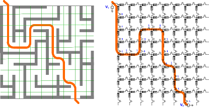
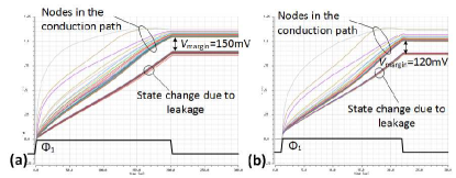
The developed memristor emulator circuit can be leveraged for system-level exploration of memcomputing and neuromorphic computing applications [17, 18], in parallel to memristive device development. Here, we apply the circuit to realize a 2D maze solver using a memristive network based on [17] and is shown in Fig. 6. Each tile of this network consists of two CMOS memristors and two NMOS switches each. This grid size network topology is generic and can be configured to a specific maze pattern by selectively opening and closing the switches in Fig. 6 [17, 3]. Initially, the states of all the memristor cells are set to zero (or high-resistance state) in simulation by initializing the respective gate voltages () to 0V. The array addressing scheme for switch configuration and state reset is not shown here. DC voltages and are applied across the desired entrance and exit nodes in the maze to solve for available paths, and the strobe is set high to allow the network to settle. The simulation results for this network are illustrated in Fig. 7, where the state voltages for each of the memristor cells are plotted as a function of time, after the strobe is applied. Here, the memristors in the path connecting the entrance and the exit, i.e. the solution of the maze, start conducting current as they decrease their respective resistances. On the other hand, the memristors in the non-conducting paths also start conducting due to leakage in the memristor circuit and the ‘sneak paths’, and their states increase as well, but at a lower rate as seen in Fig. 7 (a&b). Eventually all state nodes try to reach closer to . The result of the network is read out by setting the strobe period such that the states of the ‘On’ memristors saturate, allowing for a voltage margin () for sensing as shown in Fig. 7. The nodes that are in the maze solution path can be determined by thresholding their states above the voltage level set by leakage currents in ‘Off’ memristors. Here, the static power consumption is around and peak dynamic current is ~ from the supply. This application circuit can be further optimized for maximizing the read margin, and the decision threshold and strobe times can be digitally calibrated to compensate for process, voltage and temperature (PVT) variations.
V Conclusion
A compact memristor emulator circuit in standard CMOS has been presented along with simulation results. The circuit exhibits the signature characteristics for ideal memristors and can transcend the challenges associated with memristive device development in the near future. Furthermore, the circuit has been applied to parallel maze solving, and paves the path for applying the concept to other NP-hard problems that can be solved by exploiting the parallel analog computation.
References
- [1] D. B. Strukov, G. S. Snider, D. R. Stewart, and R. S. Williams, “The missing memristor found,” Nature, vol. 453, no. 7191, pp. 80–83, 2008.
- [2] A. Rothenbuhler, T. Tran, E. H. Barney Smith, V. Saxena, and K. A. Campbell, “Reconfigurable threshold logic gates using memristive devices,” Journal of Low Power Electronics and Applications, vol. 3, no. 2, pp. 174–193, 2013.
- [3] I. Vourkas and G. C. Sirakoulis, Memristor-based nanoelectronic computing circuits and architectures. Springer, 2016.
- [4] D. Kuzum, R. G. Jeyasingh, B. Lee, and H.-S. P. Wong, “Nanoelectronic programmable synapses based on phase change materials for brain-inspired computing,” Nano letters, vol. 12, no. 5, pp. 2179–2186, 2011.
- [5] S. H. Jo, K.-H. Kim, and W. Lu, “High-density crossbar arrays based on a si memristive system,” Nano letters, vol. 9, no. 2, pp. 870–874, 2009.
- [6] G. Indiveri, R. Legenstein, G. Deligeorgis, and T. Prodromakis, “Integration of nanoscale memristor synapses in neuromorphic computing architectures,” Nanotechnology, vol. 24, no. 38, p. 384010, 2013.
- [7] D. B. Strukov and K. K. Likharev, “A reconfigurable architecture for hybrid cmos/nanodevice circuits,” in Proceedings of the 2006 ACM/SIGDA 14th international symposium on Field programmable gate arrays. ACM, 2006, pp. 131–140.
- [8] X. Wu, V. Saxena, and K. Zhu, “Homogeneous spiking neuromorphic system for real-world pattern recognition,” IEEE Journal on Emerging and Selected Topics in Circuits and Systems, vol. 5, no. 2, pp. 254–266, 2015.
- [9] X. Wu and V. Saxena, “Enabling Bio-Plausible Multi-level STDP using CMOS Neurons with Dendrites and Bistable RRAMs,” in International Joint Conference on Neural Networks (IJCNN), Alaska, USA, May 2017.
- [10] V. Saxena, X. Wu, I. Srivastava, and K. Zhu, “Towards spiking neuromorphic system-on-a-chip with bio-plausible synapses using emerging devices,” in Proceedings of the 4th ACM International Conference on Nanoscale Computing and Communication. ACM, 2017, p. 18.
- [11] L. Chua, “Memristor-the missing circuit element,” IEEE Transactions on circuit theory, vol. 18, no. 5, pp. 507–519, 1971.
- [12] L. O. Chua and S. M. Kang, “Memristive devices and systems,” Proceedings of the IEEE, vol. 64, no. 2, pp. 209–223, 1976.
- [13] A. G. Radwan and M. E. Fouda, “Memristor: Models, types, and applications,” in On the Mathematical Modeling of Memristor, Memcapacitor, and Meminductor. Springer, 2015, pp. 13–49.
- [14] Y. N. Joglekar and S. J. Wolf, “The elusive memristor: properties of basic electrical circuits,” European Journal of Physics, vol. 30, no. 4, p. 661, 2009.
- [15] C. Yakopcic, T. M. Taha, G. Subramanyam, R. E. Pino, and S. Rogers, “A memristor device model,” Electron Device Letters, IEEE, vol. 32, no. 10, pp. 1436–1438, 2011.
- [16] L. Chua, “Resistance switching memories are memristors,” Applied Physics A, vol. 102, no. 4, pp. 765–783, 2011.
- [17] Y. V. Pershin and M. Di Ventra, “Solving mazes with memristors: A massively parallel approach,” Physical Review E, vol. 84, no. 4, p. 046703, 2011.
- [18] F. L. Traversa and M. Di Ventra, “Polynomial-time solution of prime factorization and np-complete problems with digital memcomputing machines,” Chaos: An Interdisciplinary Journal of Nonlinear Science, vol. 27, no. 2, p. 023107, 2017.
- [19] T. Serrano-Gotarredona, T. Masquelier, T. Prodromakis, G. Indiveri, and B. Linares-Barranco, “STDP and STDP variations with memristors for spiking neuromorphic learning systems.” Frontiers in neuroscience, vol. 7, no. February, p. 2, Jan. 2013.
- [20] X. Wu, V. Saxena, K. Zhu, and S. Balagopal, “A cmos spiking neuron for brain-inspired neural networks with resistive synapses and in situ learning,” IEEE Transactions on Circuits and Systems II: Express Briefs, vol. 62, no. 11, pp. 1088–1092, 2015.
- [21] E. Neftci, C. Augustine, S. Paul, and G. Detorakis, “Event-driven random back-propagation: Enabling neuromorphic deep learning machines,” arXiv preprint arXiv:1612.05596, 2016.
- [22] R. Waser, R. Dittmann, G. Staikov, and K. Szot, “Redox-based resistive switching memories–nanoionic mechanisms, prospects, and challenges,” Advanced materials, vol. 21, no. 25-26, pp. 2632–2663, 2009.
- [23] S. Yu, X. Guan, and H.-S. P. Wong, “On the stochastic nature of resistive switching in metal oxide rram: Physical modeling, monte carlo simulation, and experimental characterization,” in Electron Devices Meeting (IEDM), 2011 IEEE International. IEEE, 2011, pp. 17–3.
- [24] D. Ielmini and R. Waser, Resistive switching: from fundamentals of nanoionic redox processes to memristive device applications. John Wiley & Sons, 2015.
- [25] D. Liu, H. Cheng, X. Zhu, G. Wang, and N. Wang, “Analog memristors based on thickening/thinning of ag nanofilaments in amorphous manganite thin films,” ACS applied materials & interfaces, vol. 5, no. 21, pp. 11 258–11 264, 2013.
- [26] K. Beckmann, J. Holt, H. Manem, J. Van Nostrand, and N. C. Cady, “Nanoscale hafnium oxide rram devices exhibit pulse dependent behavior and multi-level resistance capability,” MRS Advances, vol. 1, no. 49, pp. 3355–3360, 2016.
- [27] V. Saxena, “Memory controlled circuit system and apparatus,” Oct. 2015, US Patent App. 14/538,600. [Online]. Available: https://www.google.com/patents/US20150278682
- [28] S. Nandakumar, M. Minvielle, S. Nagar, C. Dubourdieu, and B. Rajendran, “A 250 mv cu/sio2/w memristor with half-integer quantum conductance states,” Nano letters, vol. 16, no. 3, pp. 1602–1608, 2016.
- [29] A. L. Fitch, Development of memristor based circuits. World Scientific, 2013, vol. 82.
- [30] Y. V. Pershin and M. Di Ventra, “Practical approach to programmable analog circuits with memristors,” IEEE Transactions on Circuits and Systems I: Regular Papers, vol. 57, no. 8, pp. 1857–1864, 2010.
- [31] B. Muthuswamy and L. O. Chua, “Simplest chaotic circuit,” International Journal of Bifurcation and Chaos, vol. 20, no. 05, pp. 1567–1580, 2010.
- [32] J. Valsa, D. Biolek, and Z. Biolek, “An analogue model of the memristor,” International Journal of Numerical Modelling: Electronic Networks, Devices and Fields, vol. 24, no. 4, pp. 400–408, 2011.
- [33] H. Kim, M. P. Sah, C. Yang, S. Cho, and L. O. Chua, “Memristor emulator for memristor circuit applications,” IEEE Transactions on Circuits and Systems I: Regular Papers, vol. 59, no. 10, pp. 2422–2431, 2012.
- [34] S. Shin, J.-M. Choi, S. Cho, and K.-S. Min, “Small-area and compact cmos emulator circuit for cmos/nanoscale memristor co-design,” Nanoscale research letters, vol. 8, no. 1, p. 454, 2013.
- [35] C. Sánchez-López, J. Mendoza-Lopez, M. Carrasco-Aguilar, and C. Muñiz-Montero, “A floating analog memristor emulator circuit,” IEEE Transactions on Circuits and Systems II: Express Briefs, vol. 61, no. 5, pp. 309–313, 2014.
- [36] C. Yang, H. Choi, S. Park, M. P. Sah, H. Kim, and L. O. Chua, “A memristor emulator as a replacement of a real memristor,” Semiconductor Science and Technology, vol. 30, no. 1, p. 015007, 2014.