Compiled October 21, 2017 \ociscodes(050.5298) Photonic crystals; (100.1160) Analog optical image processing.
A Photonic Crystal Slab Laplace Differentiator
Abstract
We introduce an implementation of a Laplace differentiator based on a photonic crystal slab that operates at transmission mode. We show that the Laplace differentiator can be implemented provided that the guided resonances near the point exhibit an isotropic band structure. Such a device may facilitate nanophotonics-based optical analog computing for image processing.
1 Introduction
In image processing, spatial differentiation accomplishes image sharpening and edge-based segmentation, with broad applications ranging from microscopy and medical imaging to industrial inspection and object detection.[1, 2, 3, 4, 5] In these applications, of particular importance are isotropic derivative operators, whose response is rotationally invariant. The simplest and most widely used isotropic derivative operator is the two-dimensional Laplacian.[6]
Spatial differentiation can certainly be carried out with conventional digital electronic computation. However, there are many big-data applications that require real-time and high-throughput image processing, for which digital computations become challenging.[7, 8] Optical analog computing may overcome this challenge by offering high-throughput derivative operation with almost no energy consumption other than the inherent optical loss associated with the differential operators.[9, 10, 11, 12, 13, 14, 15, 16, 17, 18, 19] Moreover, the recent developments of nanophotonic structures such as meta-surfaces and plasmonic structures have offered the possibility of doing optical differentiation using compact devices. However, most of the existing works on optical spatial differentiation using nanophotonic structures are restricted to one dimension, whereas most images are two-dimensional objects.[20, 21, 22, 23, 24, 25, 26] To date, there has been no optical realization of the two-dimensional Laplacian at transmission mode with a compact nanophotonic device.
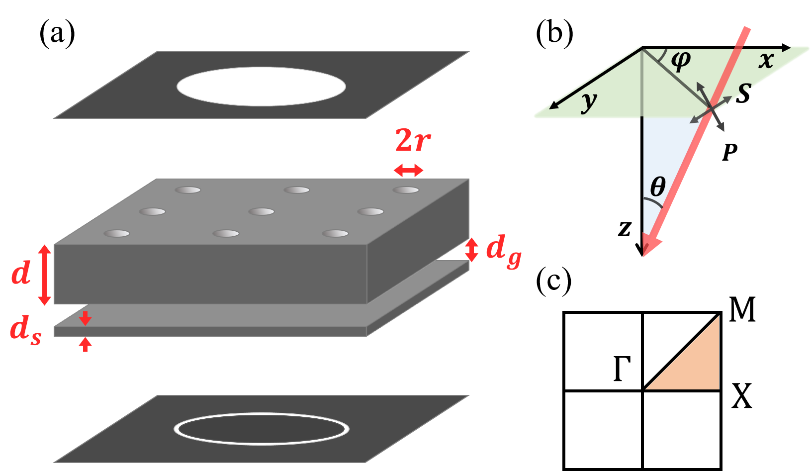
In this article, we show that a two-dimensional Lapacian can be implemented with the use of a photonic crystal slab, one of the most widely studied nanophotonic structures.[27, 28, 29] As shown in Figure 1, the structure consists of a photonic crystal slab separated from a uniform dielectric slab by an air gap. The key in this design is to achieve an unusual band structure that is isotropic for the two polarizations.
2 Theoretical Analysis
Our objective is to realize a Lapacian for a two-dimensional input field. Specifically, for a normally incident light beam along the -axis with a transverse field profile , we would like to design an optical device for which the transmitted beam has a profile , whre is the Laplacian. The task of realizing the Laplacian in the real space is equivalent to designing an optical system with response function
| (1) |
in the wavevector space (-space).[30] Equation (1) requires that at . In a lossless photonic crystal slab, the transmission for normally incident light can vanish near a guided resonance.[31] Thus we consider in more details the transmission coefficient of a photonic crystal slab near normal incidence. Consider a single photonic band of guided resonances, as characterized by -dependent resonant frequencies and radiative linewidths . (Here refers to the in-plane wavevector.) Near the resonant frequencies, the transmitted amplitude is expressed as [31]
| (2) |
where is the incident light frequency, is the direct transmission coefficient, and is related to the complex decaying amplitude of the resonance to the transmission side of the slab.
In general, is constrained by the direct process due to energy conservation and time-reversal symmetry.[31, 32] In particular, if , that is, the direct pathway has a transmission coefficient, then
| (3) |
even for structure without z-mirror symmetry such as shown in Figure 1, as has been derived in Ref. [32]. In this special case,
| (4) |
We denote , . Using Equation (4), zero transmission occurs at the point when the incident wave has the frequency:
| (5) |
At , we perform an expansion of the transmission coefficient near :
| (6) |
where
| (7) |
| (8) |
therefore,
| (9) |
In this special case, is simply proportional to the band dispersion near . If , then as well. Therefore the transmission through a photonic crystal slab can be used to achieve the Laplacian.
The analysis above indicates that, to use a photonic crystal slab as a two-dimensional spatial differentiator, it is sufficient that the slab satisfies the following three conditions:
-
1.
.
-
2.
Only one guided resonance band is coupled.
-
3.
The band satisfies the dispersion .
To satisfy the first condition above, we note that the direct transmission coefficient is related to the non-resonant transmission pathway [31]. Hence it is possible to realize by, e.g. changing the thickness of the slab. In the structure as shown in Figure 1, we achieve by placing a uniform dielectric slab in the vicinity of the photon crystal slab, and by tuning the distance between the slabs. This has the advantage that we can tune without significantly affecting the band structure of the photonic crystal slab.
To satisfy the second and third conditions above, one will need to design the band structure for the photonic crystal slab. The design here is in fact quite non-trivial due to the vectorial nature of electromagnetic waves. Since the Laplacian is isotropic in -space, it is natural to consider a photonic crystal slab structure that has rotational symmetry. As an illustration, here we consider a slab structure with a square lattice of air holes that has symmetry. For such a slab, it is known that at the point, which corresponds to , the only modes that can couple to external plane wave must be two-fold degenerate, belonging to a two-dimensional irreducible representation of the group.[33, 31] Near such modes, in the vicinity of point, the band structure in general can be described by the following effective Hamiltonian: (See Supplementary Materials)
| (10) |
where are three complex coefficients, the ’s are the Pauli matrices. This Hamiltonian has two eigenvalues of
| (11) |
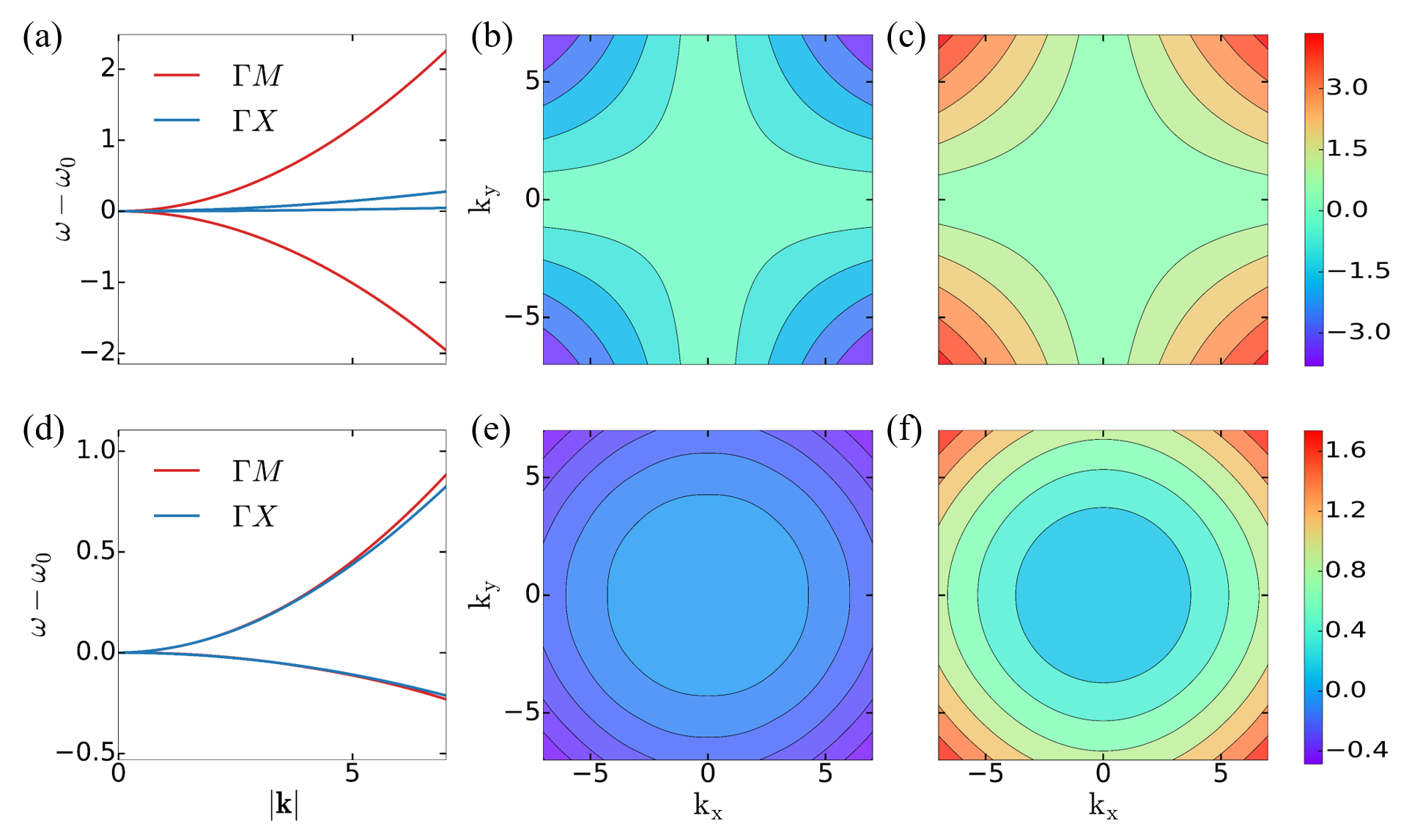
The band structure as described by Equation (11) in general does not satisfy the conditions for ideal spatial differentiation as outlined above. In this paper for concreteness we will fix the dielectric constant of the material for the slabs to be , which approximates that of Si or GaAs in the infrared wavelength range. In Figure 2(a-c), we plot the band structure for a slab with a thickness , and a radius of the holes, in the vicinity of a guided resonance at the point with a frequency . The band structure is numerically determined using guided-mode expansion method [34, 35], and it agrees excellently with the analytic expression of Equation (11) (See Supplementary Materials). At the point, the bands are two-fold degenerate. Away from the point, the degeneracy is lifted, and the two bands are strongly anisotropic, as can be seen in Figure 2(a), where the effective masses along the and the direction are drastically different. The band anisotropy can also be visualized in the constant frequency contour plotted in Figure 2(b) and (c), for the two bands. In general, it can be shown that, for a general choice of parameters , and , the constant frequency contour as described by Equation (11) is not a circle even at the limit.
On the other hand, Equation (11) also indicates that when , both bands will be isotropic:
| (12) |
To achieve such an isotropic band structure requires detailed tuning of the parameters. Numerically, we found that such an isotropic band structure can be approximately achieved with the same slab as indicated above, but near the guided resonance at with a different frequency , where the complex coefficients , thus . (See Supplementary Materials for details.) The resulting isotropic band structures are shown in Figure 2(d-f). In Figure 2(d), we see that the bands along the and direction have almost identical effective masses. And in Figure 2(e) and (f), we see that the constant frequency contours are almost completely circular.
As we mentioned above, for a structure with symmetry, the modes that a normally-incident plane wave can couple to at the point are always two-fold degenerate. Consequently, near the point, there are always two bands of guided resonance present. Moreover, off the normal direction, if the direction of incident waves is away from the high symmetry planes, both and polarized lights may couple to both bands, leading to complex polarization conversion effects. Thus, in general, in addition to having an anisotropic band structure near , a photonic crystal slab structure also does not satisfy the condition 2 above regarding the excitation of a single guided resonance band. Remarkably, however, below we show that once the condition for an isotropic band is satisfied, each of the two bands in fact only couple to one single polarization, for every direction of incidence. Below, we refer to this effect, where each polarization excites only a single band away from normal incidence, as the effect of single-band excitation.
To illustrate the effect of single-band excitation for every direction when the bands are isotropic, we first show that single-band excitation always occurs when the incident direction is in a mirror symmetry plane of the structure. Using the group theory notation in Ref. [36], as our system possesses symmetry, the doubly degenerate states at are modes. Along the direction, this pair of modes splits into two singly degenerate states of and modes which are even and odd, respectively, with respect to the reflection operator associated with the mirror plane . On the other hand, since the and polarized lights are also odd and even with respect to the same mirror plane, respectively, along the direction, the () polarized light can only couple to the () modes. Thus, in general, we have the effect of single-band excitation when the direction of incidence is in a high symmetry plane such as the plane.[37]
Next, we prove the following statement: if the two-band Hamiltonian is isotropic, that is,
| (13) |
for every , then we have the effect of single-band excitation along all directions. Here, and are the rotation operators that describe the rotation around the -axis by an angle , in the space and the two-dimensional Hilbert space, respectively. To prove this, we denote the eigenstates of the two bands as and , which connect to the and modes along the direction respectively. Equation (13) implies that:
| (14) |
We denote the and polarized modes as and respectively. By definition,
| (15) |
For along the direction, () mode does not couple to the () polarizations, i.e.
| (16) |
Then for along any direction, using Equations (14) and (15), we also have
| (17) |
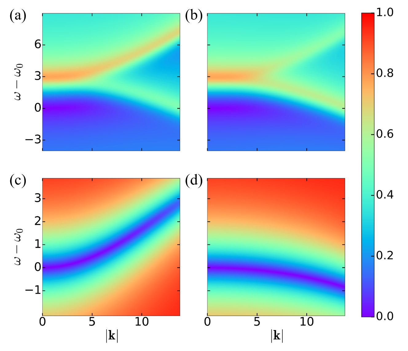
As a numerical demonstration of the connection of the single-band excitation effect with the isotropic band structure, we consider the two-slab structure as illustrated in Figure 1. The photonic crystal slab structure has the same parameters as those of Figure 2. The uniform dielectric slab has a thickness of . The air gap between the two slabs has a width of . Figure 3 shows the transmission coefficients through the two slab system, as we vary the in-plane wavevector, while maintaining , and hence the direction of the incident light is away from any symmetry plane. Near the frequency of , which is near the guided resonances as shown in Figure 2(a-c), the band structure is strongly anisotropic, and both the and polarizations excite both bands as shown in Figure 3(a-b). On the other hand, near the frequency of , which is near the guided resonances as shown in Figure 2(d-f), each polarization excites only one band as shown in Figure 3(c-d).
In this structure, the thickness of the uniform dielectric slab and the gap size are chosen such that near . Therefore, we have designed a structure that satisfies all the sufficient conditions for achieving an ideal Laplacian spatial differentiator.
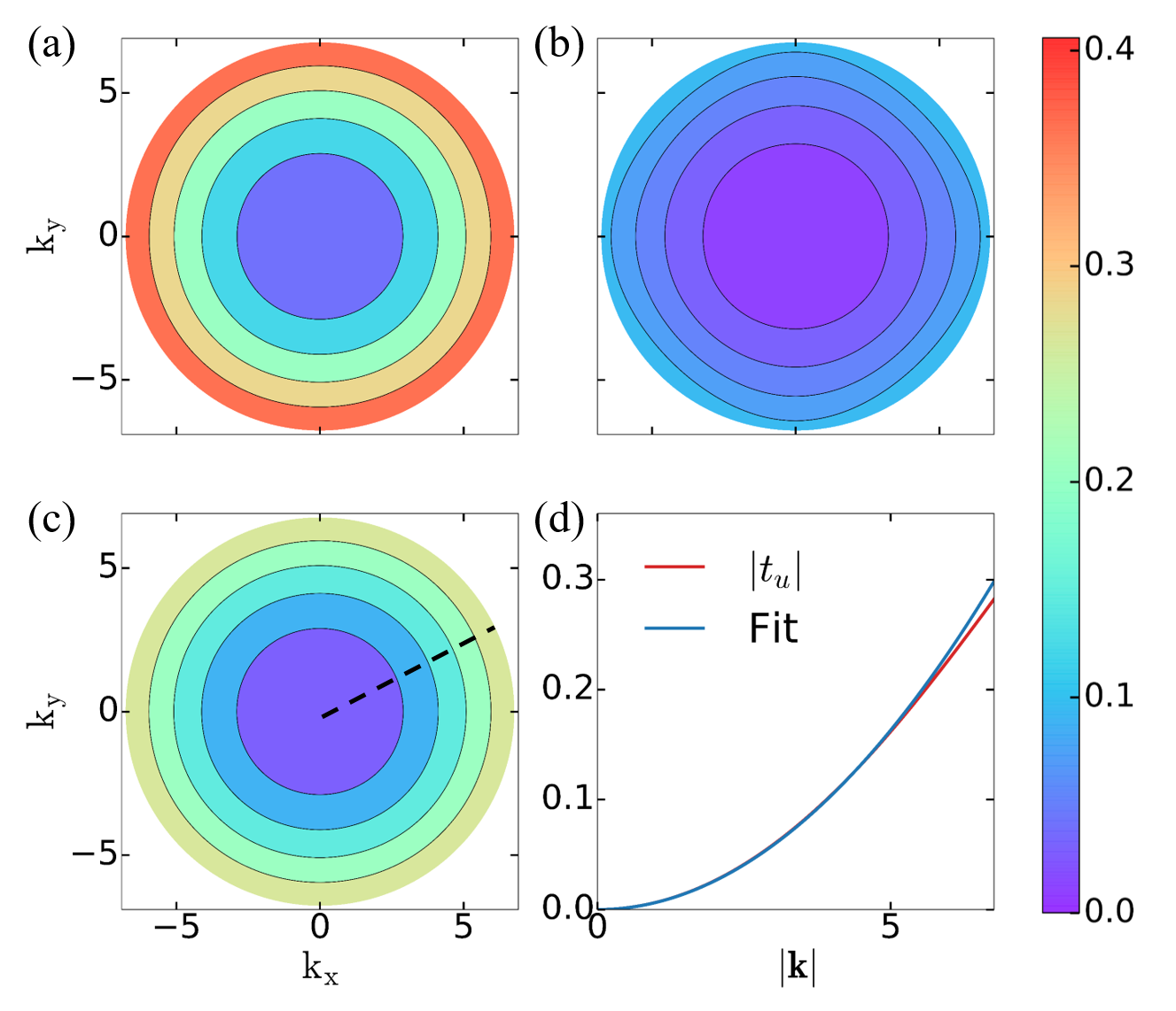
In Figure 4(a) and (b), we plot the transmission coefficients, as a function of in-plane wavevector , for the and polarized incident light, at the frequency , for the same structure used in Figure 3. Both polarizations exhibit a transmission coefficient that is proportional to . In Figure 4(c), we plot the transmission coefficient for unpolarized light at the same frequency. The transmission coefficient for the unpolarized light can be derived as (See Supplementary Materials for a derivation)
| (18) |
Here and are the transmission coefficients for and light respectively. The transmission coefficient for the unpolarized light also shows an isotropic response. In Figure 4(d), we plot as a function of , which shows a quadratic dependency. To show this, we fit the curve with quadratic function , where is the only fitting parameter. The fitting is almost perfect for up to , which as we will show provides a sufficient range of wavevector for image differentiation. Thus, the transmission coefficients have all the required -dependency in order to demonstrate a Laplacian.
3 Numerical Demonstration
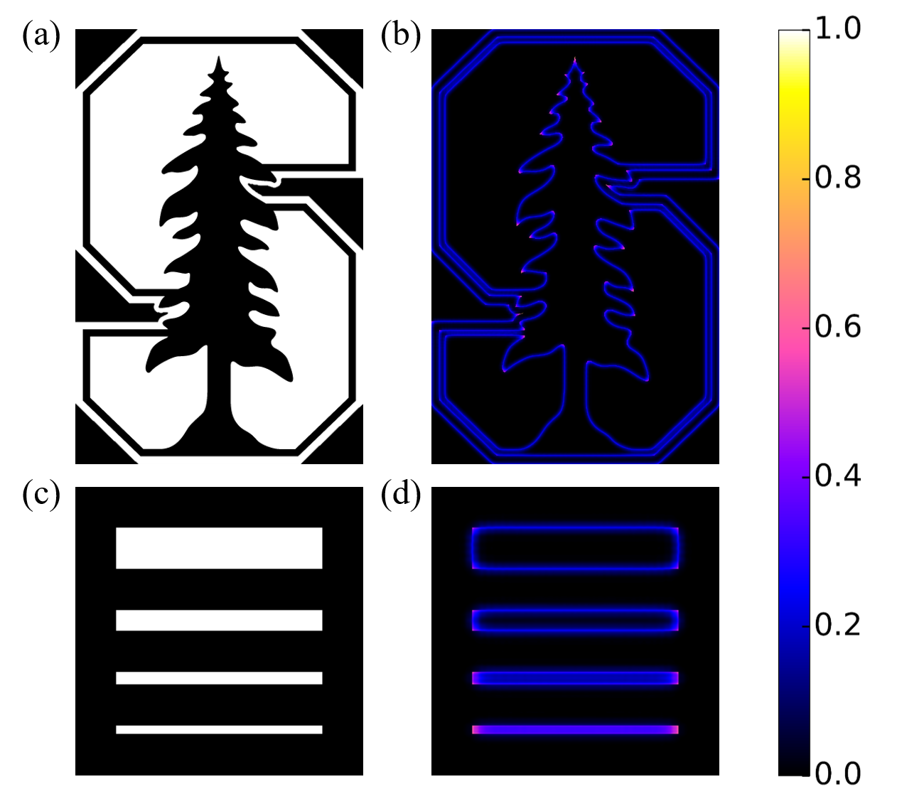
We now show that the structure used in Figure 3 indeed operates as a two-dimensional Laplacian differentiator. Figure 5(a) is the Stanford emblem as the incident image. Figure 5(b) is the calculated transmitted image, which clearly shows all the edges with the same intensity despite different edge orientations. The ability to detect edges with different orientations is a significant advantage of an isotropic differential operator such as the two-dimensional Lapacian, as compared with the one-dimensional differential operators. The Laplacian also highlights the sharp corners, exhibiting its higher sensibility to fine details as a second-order derivative operator.[1]
We also test the spatial resolution of such spatial differentiator. Figure 5(c) is a series of slot patterns and Figure 5(d) is the calculated differentiated image. The performance of edge detection degrades as the slot width decreases. The spatial resolution of our differentiator, which is the minimum separation between the two edges that can be resolved, is around . Considering corresponding to the resonant wavelength , the spatial resolution is , which is sufficient for most image processing application.
4 Discussion and Conclusion
In previous works, the two-dimensional Laplace operator has been implemented using holograms [38, 39] and phase-shifted Bragg grating [40]. These implementations either rely upon bulky optical components, or operate in reflection modes. In contrast, here we show this operation can be achieved with a compact optical structure in transmission mode, which is more compatible for image processing applications.
In conclusion, we have shown that a Laplace differentiator can be implemented using a photonic crystal slab. Such a simple photonic device may have various applications involving image processing. Future research will be worthy to extend the Laplace differentiator to multi-frequency with multi-layer structures, enabling differentiation of color images.
Funding Information
This work is supported in part by Samsung Electronics, and by the U. S. Air Force Grant No. FA9550-17-1-0002.
Acknowledgments
The authors thank Yu Guo and Dr. Alexander Cerjan for helpful discussions.
Supplementary Materialsal Documents
See Supplementary Materials for supporting content.
References
- [1] R. Gonzales and R. Woods, Digital Image Processing (Pentice Hall, NJ, 2008), 3rd ed.
- [2] R. Markham, S. Frey, and G. Hills, “Methods for the enhancement of image detail and accentuation of structure in electron microscopy,” Virology 20, 88–102 (1963).
- [3] M. D. Abràmoff, P. J. Magalhães, and S. J. Ram, “Image processing with ImageJ,” Biophotonics Int. 11, 36–42 (2004).
- [4] T. Brosnan and D. W. Sun, “Improving quality inspection of food products by computer vision - A review,” J. Food Eng. 61, 3–16 (2004).
- [5] N. Dalal and B. Triggs, “Histograms of oriented gradients for human detection,” in “Comput. Vis. Pattern Recognition, 2005. CVPR 2005. IEEE Comput. Soc. Conf.”, (IEEE, 2005), pp. 886–893.
- [6] A. Rosenfeld and A. C. Kak, Digital Picture Processing (Academic Press, New York, 1982).
- [7] D. L. Pham, C. Xu, and J. L. Prince, “Current Methods in Medical Image Segmentation,” Annu. Rev. Biomed. Eng. 2, 315–337 (2000).
- [8] R. J. Holyer and S. H. Peckinpaugh, “Edge detection applied to satellite imagery of the oceans,” IEEE Trans. Geosci. Remote Sens. 27, 46–56 (1989).
- [9] D. R. Solli and B. Jalali, “Analog optical computing,” Nat. Photonics 9, 704–706 (2015).
- [10] D. Görlitz and F. Lanzl, “A Holographic Spatial Filter for Direction Independent Differentiation,” Jpn. J. Appl. Phys. 14, 223 (1975).
- [11] J. Eu, C. Liu, and A. Lohmann, “Spatial filters for differentiation,” Opt. Commun. 9, 168–171 (1973).
- [12] E. R. Reinhardt and W. H. Bloss, “Optical Differential Operation Processor,” Opt. Eng. 17, 69–72 (1978).
- [13] R. Sirohi and V. R. Mohan, “Differentiation by Spatial Filtering,” Opt. Acta Int. J. Opt. 24, 1105–1113 (1977).
- [14] H. Kasprzak, “Differentiation of a noninteger order and its optical implementation,” Appl. Opt. 21, 3287 (1982).
- [15] S. K. Yao and S. H. Lee, “Spatial Differentiation and Integration by Coherent Optical-Correlation Method,” J. Opt. Soc. Am. 61, 474 (1971).
- [16] K. S. Nesteruk, I. P. Nikolaev, and A. V. Larichev, “Image differentiation with the aid of a phase knife,” Opt. Spectrosc. 91, 295–299 (2001).
- [17] C. Warde and J. Thackara, “Operating Modes Of The Microchannel Spatial Light Modulator,” Opt. Eng. 22, 695–703 (1983).
- [18] J. A. Davis, W. V. Brandt, D. M. Cottrell, and R. M. Bunch, “Spatial image differentiation using programmable binary optical elements,” Appl. Opt. 30, 4610 (1991).
- [19] J. Lancis, T. Szoplik, E. Tajahuerce, V. Climent, and M. Fernández-Alonso, “Fractional derivative Fourier plane filter for phase-change visualization.” Appl. Opt. 36, 7461–4 (1997).
- [20] T. Zhu, Y. Zhou, Y. Lou, H. Ye, M. Qiu, Z. Ruan, and S. Fan, “Plasmonic computing of spatial differentiation,” Nat. Commun. 8, 15391 (2017).
- [21] N. V. Golovastikov, D. A. Bykov, L. L. Doskolovich, and V. A. Soifer, “Spatiotemporal optical pulse transformation by a resonant diffraction grating,” J. Exp. Theor. Phys. 121, 785–792 (2015).
- [22] N. V. Golovastikov, D. A. Bykov, and L. L. Doskolovich, “Resonant diffraction gratings for spatial differentiation of optical beams,” Quantum Electron. 44, 984–988 (2014).
- [23] A. Silva, F. Monticone, G. Castaldi, V. Galdi, A. Alu, and N. Engheta, “Performing Mathematical Operations with Metamaterials,” Science. 343, 160–163 (2014).
- [24] A. Youssefi, F. Zangeneh-Nejad, S. Abdollahramezani, and A. Khavasi, “Analog computing by Brewster effect,” Opt. Lett. 41, 3467 (2016).
- [25] S. AbdollahRamezani, K. Arik, A. Khavasi, and Z. Kavehvash, “Analog computing using graphene-based metalines,” Opt. Lett. 40, 5239 (2015).
- [26] A. Pors, M. G. Nielsen, and S. I. Bozhevolnyi, “Analog Computing Using Reflective Plasmonic Metasurfaces,” Nano Lett. 15, 791–797 (2015).
- [27] E. Chow, S. Y. Lin, S. G. Johnson, P. R. Villeneuve, J. D. Joannopoulos, J. R. Wendt, G. a. Vawter, W. Zubrzycki, H. Hou, and A. Alleman, “Three-dimensional control of light in a two-dimensional photonic crystal slab.” Nature 407, 983–986 (2000).
- [28] J. D. Joannopoulos, S. G. Johnson, J. N. Winn, and R. D. Meade, Photonic crystals: molding the flow of light (Princeton university press, 2011).
- [29] W. Zhou, D. Zhao, Y.-C. Shuai, H. Yang, S. Chuwongin, A. Chadha, J.-H. Seo, K. X. Wang, V. Liu, Z. Ma, and S. Fan, “Progress in 2D photonic crystal Fano resonance photonics,” Prog. Quantum Electron. 38, 1–74 (2014).
- [30] R. N. Bracewell and R. N. Bracewell, The Fourier transform and its applications, vol. 31999 (McGraw-Hill New York, 1986).
- [31] S. Fan and J. D. Joannopoulos, “Analysis of guided resonances in photonic crystal slabs,” Phys. Rev. B 65, 235112 (2002).
- [32] K. X. Wang, Z. Yu, S. Sandhu, and S. Fan, “Fundamental bounds on decay rates in asymmetric single-mode optical resonators,” Opt. Lett. 38, 100 (2013).
- [33] T. Ochiai and K. Sakoda, “Dispersion relation and optical transmittance of a hexagonal photonic crystal slab,” Phys. Rev. B 63, 125107 (2001).
- [34] L. C. Andreani and D. Gerace, “Photonic-crystal slabs with a triangular lattice of triangular holes investigated using a guided-mode expansion method,” Phys. Rev. B 73, 235114 (2006).
- [35] M. Minkov and V. Savona, “Automated optimization of photonic crystal slab cavities,” Sci. Rep. 4, 5124 (2015).
- [36] K. Sakoda, Optical Properties of Photonic Crystals, vol. 80 of Springer Series in Optical Sciences (Springer-Verlag, Berlin, Heidelberg, 2005).
- [37] S. G. Tikhodeev, A. L. Yablonskii, E. A. Muljarov, N. A. Gippius, and T. Ishihara, “Quasiguided modes and optical properties of photonic crystal slabs,” Phys. Rev. B 66, 045102 (2002).
- [38] C.-S. Guo, Q.-Y. Yue, G.-X. Wei, L.-L. Lu, and S.-J. Yue, “Laplacian differential reconstruction of in-line holograms recorded at two different distances,” Opt. Lett. 33, 1945 (2008).
- [39] J. P. Ryle, D. Li, and J. T. Sheridan, “Dual wavelength digital holographic Laplacian reconstruction,” Opt. Lett. 35, 3018 (2010).
- [40] D. A. Bykov, L. L. Doskolovich, E. A. Bezus, and V. A. Soifer, “Optical computation of the Laplace operator using phase-shifted Bragg grating,” Opt. Express 22, 25084 (2014).