Radiation Hardness of Thin Low Gain Avalanche Detectors
Abstract
Low Gain Avalanche Detectors (LGAD) are based on a n++-p+-p-p++ structure where an appropriate doping of the multiplication
layer (p+) leads to high enough electric fields for impact ionization. Gain factors of few tens in charge
significantly improve the resolution of timing measurements, particularly for thin detectors,
where the timing performance was shown to be limited by Landau fluctuations. The main obstacle
for their operation is the decrease of gain with irradiation, attributed to effective acceptor removal in the gain layer. Sets of thin
sensors were produced by two different producers on different substrates, with different gain layer doping profiles and thicknesses (45, 50 and 80 m).
Their performance in terms of gain/collected charge and leakage current was compared before and after irradiation with neutrons and
pions up to the equivalent fluences of cm-2. Transient Current Technique and charge collection measurements with LHC
speed electronics were employed to characterize the detectors. The thin LGAD sensors were shown to perform much better than sensors of standard
thickness (300 m) and offer larger charge collection with respect to detectors without gain layer for fluences cm-2. Larger initial gain prolongs the beneficial performance of LGADs.
Pions were found to be more damaging than neutrons at the same equivalent fluence, while no significant difference was found between different producers. At very high fluences and bias voltages
the gain appears due to deep acceptors in the bulk, hence also in thin standard detectors.
PACS: 85.30.De; 29.40.Wk; 29.40.Gx
keywords:
Silicon detectors, Full depletion voltage, Radiation damage, Signal multiplication1 Introduction
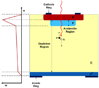
Low gain avalanche detectors (LGAD) exploit a n++-p+-p-p++ structure to achieve high enough electric fields near the junction contact for impact ionization [1] (see Fig. 1). The gain depends on the p+ layer’s doping level and profile shape. Usually gain factors of several tens were achieved in most LGADs produced so far.
That assures efficient operation of thin sensors required for precise timing applications in particle physics [2]. A superb timing resolution of 26 ps per single LGAD layer was achieved recently [3], which made thin LGADs ( m) a baseline option for timing detectors of both CMS and ATLAS at the high luminosity upgrade of the LHC (HL-LHC) around 2026 [4, 5]. The main obstacle for their successful use at future experiments in high energy physics is the degradation of gain with fluence. LGADs will be exposed at the HL-LHC to equivalent fluences of up to cm-2. At these fluences the gain due to the p+ layer completely disappears [6].
Excellent timing resolution can only be achieved if the induced current variations due to Landau fluctuations are minimized, therefore the use of thin devices is required [7].
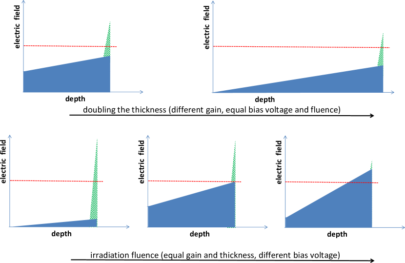
The use of thin devices also improves the radiation hardness as explained in the following. After the device depletes the further increase of bias voltage roughly increases the electric field by the same amount over the entire thickness of the device. This requires a much higher bias voltage in 300 m thick LGAD detectors than in thin ones to retain high electric fields in the gain region. The device usually breaks down before the gain can be recovered. With an appropriate design a thin sensor tolerating a high bias voltage would therefore be more radiation hard, although only because of geometrical effect. This is illustrated in Fig. 2. At very high fluences the concentration of initial acceptors in the gain layer becomes negligible, but the deep acceptors created in the part of the bulk by irradiation lead to fields high enough for sizable multiplication as observed before [8, 9, 10].
In order to test this hypothesis and to establish the requirements needed for successful operation of thin LGAD sensors, sets of different thin LGADs produced by CNM111Centro Nacional de Microelectrónica, Barcelona, Spain and HPK 222Hamamatsu Photonics, Hamamatsu, Japan were characterized before and after irradiations with different particles. The timing measurements with these LGADs are presented in other papers [11, 12]. It was found that after low and moderate fluences ( cm-2) the gain solely determines the timing resolution once the velocities close to saturation are achieved in the detector bulk (provided the noise is constant). Moreover at very high fluences the multiplication taking place in the bulk instead of in a narrow gain layer results in faster induced current rise, therefore improved timing resolution even at somewhat smaller gain. Establishing the relation between the collected charge and the required operation voltage in the complete fluence range of HL-LHC is therefore of utmost importance. While most of the recent irradiation studies concentrated on reactor neutrons, LGADs at HL-LHC will be exposed also to charged hadrons which were shown before [6] to cause faster effective acceptor removal at the same equivalent fluence. Therefore LGADs studied in the present work include also those irradiated by 200 MeV pions.
Comparison of devices of different thicknesses will also add to the understanding of the underlying mechanism of effective acceptor removal. The dependence of the effective acceptor removal rate on different producers will show its universality and possibly lead to improved doping profiles. Thin LGADs made on different substrates will also reveal their impact on charge collection.
2 Samples and experimental technique
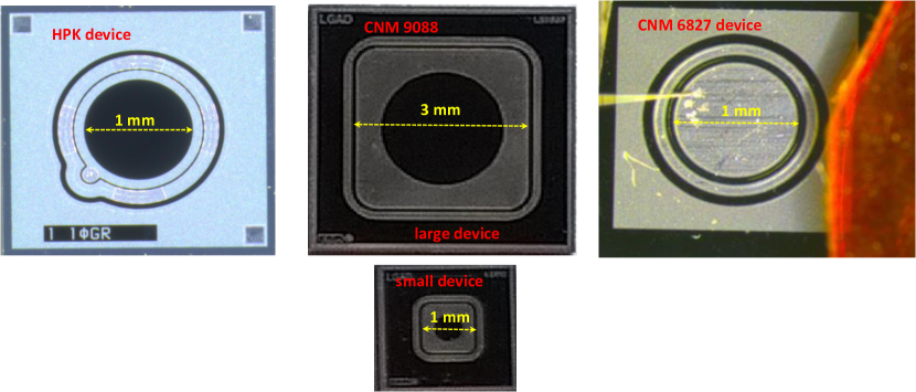
Three different sets of LGADs produced by CNM and HPK were studied with their properties listed in Table 1 and shown in Fig. 3.
| Sample set/Run | Producer | size-thickness | Implantation Dose | substrate |
|---|---|---|---|---|
| R9088 | CNM | rectangular | L = cm-2 | 300 m SOI |
| L = mm - 45 m | M = cm-2 | |||
| S = mm - 45 m | H = cm-2 | |||
| R6827 | CNM | circular mm - 50 m | cm-2 | 300 m EPI |
| ECX20840 | HPK | circular mm - 50 m | A,B,C,D | 300 m |
| or short | circular mm - 80 m | 4% between splits | low resistivity | |
| HPK | A-lowest, D-highest | Si wafer |
All three sets were irradiated with neutrons at Jožef Stefan Institute research reactor [13]. Set R9088 was irradiated also with 200 MeV pions at Paul Scherrer Institute in Villigen, Switzerland [14]. They were characterized by Transient Current Technique (TCT) [15] and charge collection efficiency measurement with electrons from a 90Sr source with LHC speed electronics (CCM). The detailed description of the setups can be found in [16] for TCT and [17] for CCM. The very small size of the active pads required a small collimator (1 mm2) which together with careful alignment assured that almost all the electrons that reach the scintillator and trigger the readout have crossed the detector. This allowed the measurements of the signal even at very low signal-to-noise (S/N) ratios. In some case for the smallest samples a non-perfect alignment was tolerated as the relatively large S/N for these devices allowed the separation of noise hits (i.e. electrons missing the active area and triggering the readout).
The measurements were performed after annealing for 80 min at 60∘C. Samples from sets HPK and R6827 were irradiated in several steps with the above mentioned annealing procedure done after each step (CERN scenario [18]). In this way it was possible to cover the fluence range with a limited number of samples. The fluences of particles were scaled to 1 MeV neutron equivalent fluences by using hardness factors: 0.92 for reactor neutrons ( keV) [19] and 1.14 for 200 MeV pions [18].
3 Charge collection/gain
Charge collection measurements were performed mostly at C. At each voltage point 2500 events (90Sr electron triggers) were recorded to disk and analyzed offline. The response of the preamplifier-shaping amplifier (25 ns peaking time) was calibrated with a non-irradiated standard n+-p pad detector and also with 59.5 keV photons from a 241Am source, which allowed absolute charge measurements.
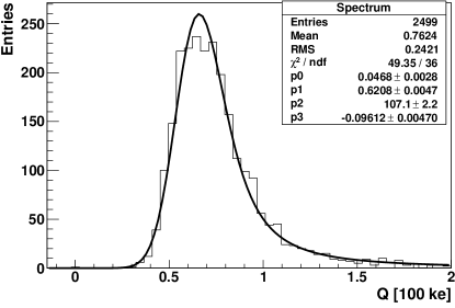
An example of a recorded spectrum for sample 9088-L-M is shown in Fig. 4. The most probable charge was extracted from the fit of the convolution of Gaussian and Landau function to the measured spectrum.
It was observed in test beam measurements of R9088 devices that there is difference in charge collection between the metallized and non-metallized part of the detector of which the origin is not clear. The difference was few percent for non-irradiated, but could be as high as few tens percent close to the break down voltage in heavily irradiated sensors. In the presented measurements we could not separate between hits of metallized and non-metallized part, therefore the average is shown.
3.1 Non-irradiated sensors
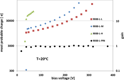
The measured signal for different investigated detectors is shown in Fig. 5. The gain of the devices is here defined as the most probable charge divided with the signal in a standard diode (PIN) of the same thickness ( e for R9088).
 |
 |
| (a) | (b) |
(c)
Gains of up to almost one hundred were achieved. A clear dependence of most probable charge on different gain layer doping concentrations can be observed. A remarkable difference given the only few percent difference between implantation doses. The control of the gain and breakdown performance requires therefore excellent process control. The benefit of thicker detectors of more generated primary charge can be (over) compensated with higher bias voltages due to average electric fields achieved leading to higher gains (see Fig. 5b). Thicker detectors also have smaller capacitance, hence noise, but the contribution due to Landau fluctuations to timing resolution is worse [2]. In addition the induced current amplitude is smaller at the same gain in thicker detectors (). Hence thicker detectors are suitable when smaller noise or limited voltage is required. The benefits of large breakdown voltages can be best seen in Fig. 5c. The R6827 device exhibits amplification only after substantial over-depletion, required to reach fields high enough for impact ionization.
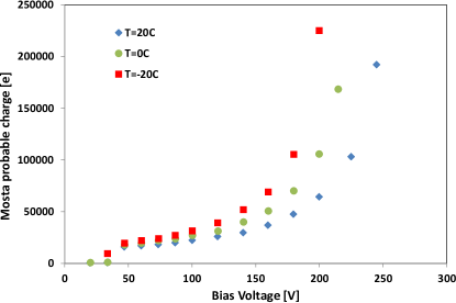
The gain dependence on temperature was investigated for R9088 medium dose devices and is shown in Fig. 6. A strong temperature dependence can be seen at high bias voltages (gains). The impact ionization coefficients become strongly temperature dependent at high fields [20]. Around 30% increase in gain can be assumed at between C and C. Influence of temperature on gain is therefore more significant in thin sensors where higher fields can be reached. Smaller gain at higher temperatures can be offset by applying higher bias as the break down voltage also increases with temperature.
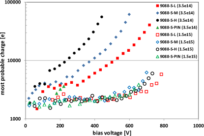
3.2 Neutron irradiated sensors
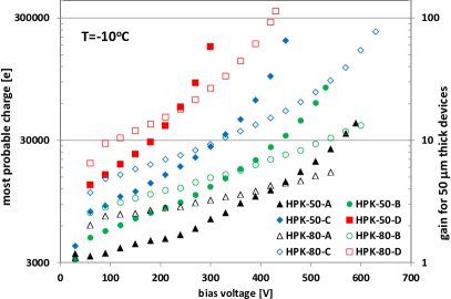
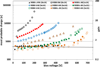
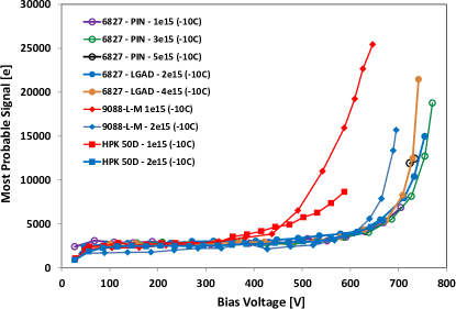
The collected charge in irradiated sensors is shown in Fig. 7. The definition of the gain requires the knowledge of for fully depleted irradiated sensor and is often replaced by for easier calculation of the charge. Only after trapping becomes substantial these two definitions differ, which for thin detectors occurs at fluences larger than few cm-2.
A large decrease of charge with fluence is evident. At lower fluences the gain is still substantial after full depletion of the device ( V) while for high fluences the gain remains visible only at highest voltages. The decrease of gain is attributed to initial acceptor removal in the multiplication layer [6] and will be addressed in the next section. The gain loss at lower fluences can be compensated by applying higher bias voltage (see Fig. 2), but a full compensation is not possible anymore at fluences cm-2.
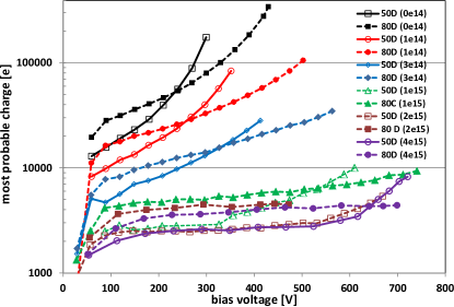
Electric fields at highest bias voltages 600-700 V (on average 12-15 V/m) are sufficient to cause multiplication in the large part of the bulk and 50 m devices break down in a very narrow voltage interval around 700 V at high fluences. Although the break-even voltage in collected charge for 50 m and 80 m devices (Fig. 7b) shifts to ever larger values due to reduced gain, thin devices nevertheless always outperform thick ones in the investigated fluence range.
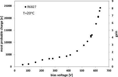
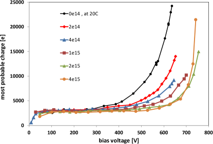
The residual concentration of initial acceptors in the gain layer plays a larger role in thin than in thick detectors after irradiation. Although not sufficient for yielding gain immediately after depletion ( is constant over a large voltage interval) they lead to improved gain at high voltages. This effect can be observed in all devices and it is best illustrated in Fig. 7c, for the devices from R6827 where the initial doping was low enough to observe this behavior already before irradiation. The increase of voltage required for the onset of multiplication with fluence can be clearly observed. At the highest two fluences ( cm-2) the collected charge dependence on voltage is almost the same. Larger concentration of deep acceptors in the bulk may even lead to larger gains at voltages close to break down voltage.
 |
 |
| (a) | (b) |
(c)
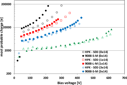
The removal of initial acceptors favors the choice of highest possible doping of the multiplication layer. This is shown in Fig. 8a, where the devices from R9088 are compared. However, although the difference still remains after cm-2, it is becoming smaller. The same observation holds also for HPK samples. At fluences above cm-2 the performance of devices becomes universal regardless of producer or initial doping, with even the same performance of the LGAD device and diodes without multiplication layer (see Fig. 8b). Moreover, there is also little effect of irradiation fluence. The effect of trapping seems to be small and with precision of our measurements is estimated to be less than 20% difference in most probable charge between non-irradiated sensors and those to cm-2 before the onset of multiplication.
 |
 |
| (a) | (b) |
The rate of initial acceptor removal depends on concentration [21], therefore different doping profiles could lead to different post irradiation gains, even when similar before irradiation. The two producers have different processes, but the comparison of devices with similar initial gain exhibited little difference in charge vs. voltage dependence as shown in Fig. 9. Whether this is a coincidence or the parameter space in device processing is so restricted that different producers converge to similar doping profile shapes remains an open question.
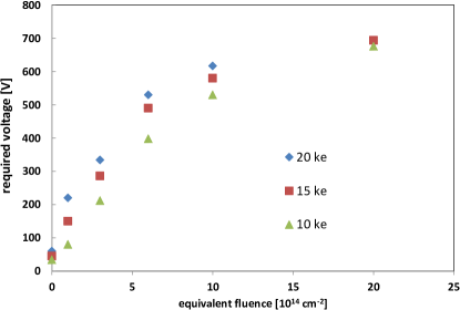
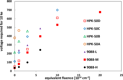
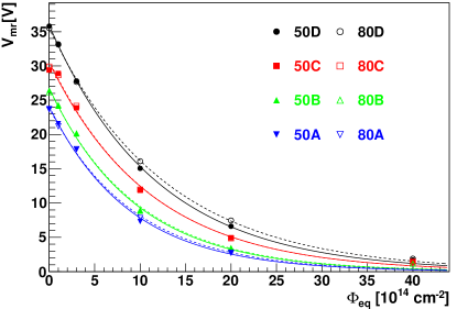
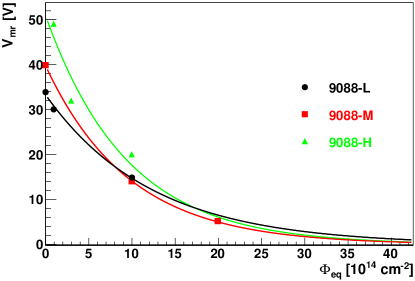
The collected charge determines to a large extent the timing resolution of the sensors once the applied voltage is sufficient to saturate the drift velocity in the entire bulk. It is assumed that shot noise and by that jitter can be kept under control, due to small foreseen integration times of 1 ns. Saturation of drift velocities requires electric fields in the bulk of few V/m. This is almost always achievable already after low fluences or for devices with lower initial gain layer doping, but not necessarily for high gain layer doping which can lead to early break down (see Fig. 5). The bias voltage therefore determines the gain and by that to a large extent the timing resolution of the devices. The figure of merit for a detector is therefore voltage required for given charge. The further the voltage is from the breakdown voltage the safer is the operation of the detector. In Fig. 10a the dependence of the required voltage for the collection of 10,15 and 20 ke is shown for R9088 devices as a function of equivalent fluence. The difference in voltage required for 10 and 20 ke is around 150 V and decreases with fluence as the charge rise becomes steeper when approaching the breakdown voltage (see Fig. 7). Timing resolution of around 50 ps corresponds roughly to 20 ke [11, 12]. The benefit of having higher initial doping concentration is shown in Fig. 10b for different detectors from sets R9088 and HPK. Therefore higher initial doping will keep the benefits of LGADs to larger fluences and would allow to operate detectors at lower voltages.
 |
 |
| (a) | (b) |
The three sets of samples were produced on different substrates, which seem not to influence the charge collection performance.
3.3 Pion irradiated CNM sensors
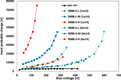
At HL-LHC radiation damage will be caused by both charged hadrons and neutrons. It is long known that at the same non-ionizing energy loss (NIEL) the damage inflicted to the detector can be different regarding the irradiation particle type (NIEL hypothesis violation) [18]. As most of the studies with irradiated LGADs were so far performed with neutrons it is important to check the acceptor removal and related loss of gain also after charged hadron irradiations. R9088 samples of all doping concentrations were irradiated with pions to equivalent fluences of cm-2 and cm-2. Measured charge vs. bias voltage for pion irradiated devices is shown in Fig. 11a. It seems that for low fluences the bulk depletes first and only then the gain layer which leads to a steep rise in collected charge. As for neutron irradiation, a higher gain is preserved for higher initial doping at medium fluence, whereas at high fluence the difference becomes small.
The required voltage for a given charge is larger for pion compared to neutron irradiated samples at comparable fluences (see Fig. 11b). The curve for pion irradiated sample to cm-2 is similar to that of the neutron irradiated one at almost double equivalent fluence ( cm-2). This is true also for samples irradiated to high fluence.
 |
 |
| (a) | (b) |
It is therefore essential to more precisely evaluate the acceptor removal after charged hadron irradiations and also mixed irradiations (charged hadron and neutron irradiations) in order to be able to make predictions of detector operation at different locations in HL-LHC experiments.
4 Leakage current
As has been shown in Ref. [6] the leakage current in LGAD devices follows
| (1) |
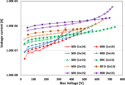
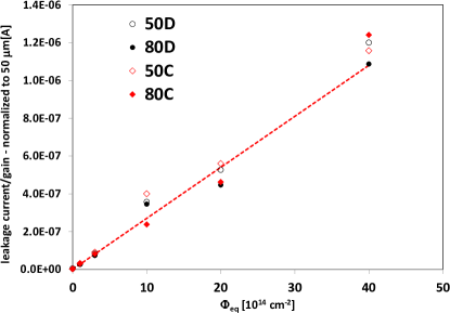
where is the generation current, the current multiplication factor, C A/cm the leakage current damage constant [18], the detector thickness and the active surface. For some samples from CNM runs the leakage current was un-usually high before irradiation which often led to a discrepancy between the calculated and measured currents [6]. The leakage current dependence on fluence is not linear as the decrease of compensates the increase of the generation current. The measured dependence of the leakage current for R9088 and HPK devices is shown in Fig. 12. With assumed to be the same as charge gain determined from charge collection measurements, the agreement between calculated and measured current for HPK sensors is within 20% (mainly from uncertainty in temperature). An average of the current measurements above the full depletion voltage divided by the gain and normalized to m thickness is shown in Fig. 12b. Such a good agreement between measured and calculated currents allows for an estimate of the gain from current measurements. The measured current in R9088-L-M samples is given in Fig. 12c and similar conclusion as for HPK sensors holds. Note that the larger current for R9088 devices than for HPK is a consequence of the different active area.
 |
 |
| (a) | (b) |

5 TCT studies of multiplication layer
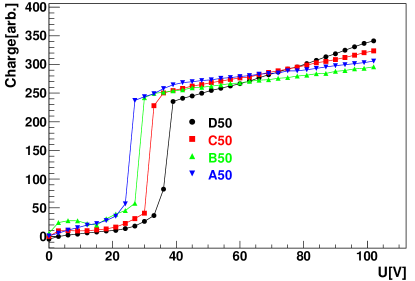
The transient current technique (TCT) is an ideal tool to study the properties of the gain layer. The voltage required to deplete the p+ layer can be probed by observing the induced currents after front illumination of the detector by light of short penetration depth (3 m at nm; pulse width FWHM400 ps, 500 Hz repetition). Once the p+ layer is depleted the induced current increases as more carriers drift. An example of induced current pulses for a non-irradiated HPK detector is shown in Fig. 13a, where the steep increase of the current at 39 V indicates the depletion of the multiplication layer. The dependence of charge (current integral in 20 ns) on bias voltage is shown in Fig. 13b. The difference in p+-layer depletion voltages for samples with different implantation doses is clearly visible. For irradiated sensors the bulk becomes highly resistive and the electrode (ground) is not effectively at the border of the depleted region anymore. Therefore the current is induced only after the carriers drift over a significant distance (weighting potential) without recombination. For constant space charge the depleted region in the p bulk grows as , and by that also the induced charge.
 |
 |
| (a) | (b) |
 |
 |
| (c) | (d) |
The voltages required for the depletion of the multiplication layer were obtained by fitting to the measured charge. As seen in Figs. 13c,d decreases with equivalent fluence. If the boron removal occurs with the same rate everywhere in the p+ layer, then is proportional to the average concentration of Boron and the evolution of with fluence can be described as
| (2) |
where is the removal constant, the initial doping concentration and the multiplication layer depletion voltage. The extracted at different fluences and the Eq. 2 fit to the data for all HPK devices are shown in Fig. 14a. The free parameters of the fit were and . It can be seen that the depletion of the layer does not depend on the device thickness. This confirms the assumption that the main mechanism of the effective acceptor removal is the deactivation of boron rather than the compensation of initial acceptors by deep donor levels. A larger concentration of thermally generated free carriers in the thicker detector would impact in the latter case. The obtained values were cm2 and V for A,B,C and D devices.
The data for R9088 are shown in Fig. 14b. The analysis here is influenced by the fact that the depletion of samples with high leakage current exhibits a so called “double junction” effect which effectively prevents an accurate determination for some of the sensors. Similar values of cm2 and V were obtained also for 9088-L,M and H devices. Given the difference of only around 12% between the maximum and minimum implantation dose for HPK and R9088 devices the reasons for significantly larger difference in are not clear to us.
The removal rates for both investigated sets are similar to those obtained previously in 300 m thick devices produced by CNM [6].
 |
 |
| (a) | (b) |
Comparable removal rates of initial acceptors for both producers point on one side to similar doping profiles for both, but also to the independence of the removal rate on all other process influenced parameters.
6 Conclusions
Systematic charge collection measurements were performed on three sets of non-irradiated and irradiated thin, 50 m and 80 m, LGAD detectors produced by CNM and HPK. The measurements showed a decrease of the collected charge/gain with fluence in agreement with initial acceptor removal in the multiplication layer. The removal rates were measured to be cm-2, compatible for both producers. These results were confirmed in charge collection measurements where a similar degradation of the collected charge with fluence was measured for both. The removal rate was found to be independent of thickness which points to the deactivation of boron as the main reason for the effective acceptor removal.
Thin LGADs retain larger charge collection than standard PIN diodes up to fluences of cm-2. The residual concentration of acceptors though insufficient to provide gain after the depletion of the p+ layer, nevertheless leads at very high bias voltages to electric fields required for impact ionization. The devices with a larger initial doping concentration of the p+ layer retain gain and moderate voltages up to larger fluences. Beyond cm-2 the behavior of LGADs becomes similar to that of standard PIN diodes. At highest biases the multiplication takes place in the bulk due to radiation induced deep acceptors, but this mode of operation is limited to voltages close to the breakdown voltage.
The leakage current follows the prediction given by the bulk generation current and the gain.
Acknowledgment
Part of this work has been financed by the Spanish Ministry of Economy and Competitiveness through the Particle Physics National Program (FPA2015-69260-C3-3-R and FPA2014-55295-C3-2-R), by the European Union’s Horizon 2020 Research and Innovation funding program, under Grant Agreement no. 654168 (AIDA-2020).
References
- [1] G. Pellegrini et al., “Technology developments and first measurements of Low Gain Avalanche Detectors (LGAD) for high energy physics applications”, Nucl. Instr. and Meth. A 765 (2014) 12.
- [2] N. Cartiglia et al., “Design optimization of ultra-fast silicon detectors”, Nucl. Instr. and Meth. A 796 (2015) 141.
- [3] N. Cartiglia et al., “Beam test results of a 16 ps timing system based on ultra-fast silicon detectors”, Nucl. Instr. and Meth. A 850 (2017) 83.
- [4] ATLAS Collaboration, “ATLAS Phase-II Upgrade Scoping Document”, CERN-LHCC-2015-020 (2015).
- [5] CMS Collaboration, “CMS Phase II Upgrade Scope Document”, CERN-LHCC-2015-19 (2015).
- [6] G. Kramberger et al., “Radiation effects in Low Gain Avalanche Detectors after hadron irradiations”, JINST Vol. 10 (2015) P07006.
- [7] H. Sadrozinski, A. Seiden, N. Cartiglia, “4-Dimensional tracking with Ultra-Fast Silicon Detectors”, ROPP-100788.R2 https://arxiv.org/abs/1704.08666 .
- [8] J. Lange et al., “Properties of a radiation-induced charge multiplication region in epitaxial silicon diodes”, Nucl. Instr. and Meth. A 622 (2010) 49.
- [9] I. Mandić et al.,“Measurement of anomalously high charge collection efficiency in n+-p strip detectors irradiated by up to neq/cm2, Nucl. Instr. and Meth. A 603 (2009) p. 263.
- [10] G. Casse, A. Affolder, P. Allport, H. Brown, and M. Wormald, “Enhanced efficiency of segmented silicon detectors of different thicknesses after proton irradiations up to neq/cm2”, Nucl. Instr. and Meth. A 624 (2010) 401.
- [11] J. Lange et al., “Gain and time resolution of 45 m thin Low Gain Avalanche Detectors”, JINST Vol. 12 (2017) P05003.
- [12] H. Sadrozinski et al., “Properties of HPK UFSD after neutron irradiation up to 6e15 n/cm2”, https://arxiv.org/abs/1707.04961.
- [13] L. Snoj, G. Žerovnik, A. Trkov, “Computational analysis of irradiation facilities at the JSI TRIGA reactor”, Appl. Radiat. Isot. 70 (2012) p. 483.
- [14] User guide to accelerator facilities, Paul Scherrer Institute, Villigen and Wurenlingen, 2nd Edition, July 1994.
- [15] V. Eremin, N. Strokan, E. Verbitskaya et al., “Development of transient current and charge techniques for the measurement of effective net concentration of ionized charges (N-eff) in the space charge region of p-n junction detectors”, Nucl. Instr. and Meth. A 372 (1996) p. 388.
- [16] G. Kramberger, V. Cindro, I. Mandić et al., “Effective trapping time of electrons and holes in different silicon materials irradiated with neutrons, protons and pions”, Nucl. Instr. and Meth. A481 (2002) 297.
- [17] G. Kramberger, V. Cindro, I. Mandić et al., “Charge collection properties of heavily irradiated epitaxial silicon detectors”, Nucl. Instr. and Meth. A554 (2005) 212.
- [18] G. Lindström on behalf of CERN-RD48 collaboration, “Radiation hard silicon detectors - developments by the RD48 (ROSE) collaboration”, Nucl. Instr. and Meth. A 466 (2001) p. 308.
- [19] D. Žontar, V. Cindro V, G. Kramberger et al., “Time development and flux dependence of neutron-irradiation induced defects in silicon pad detectors”, Nucl. Instr. and Meth. A 426 (1999) p. 51.
- [20] W.Maes, K.De Meyer, R.Van Overstraeten, “Impact ionization in silicon: A review and update”, Solid-State Elec. Vol. 33(6) (1990), p. 705.
- [21] I. Mandić et al.,”Neutron irradiation test of depleted CMOS pixel detector prototypes”, JINST Vol. 12 (2017) P02021.