Mode mixing induced by disorder in graphene PNP junction in a magnetic field
Abstract
We study the electron transport through the graphene PNP junction under a magnetic field and show that modes mixing plays an essential role. By using the non-equilibrium Green’s function method, the space distribution of the scattering state for a specific incident modes as well the elements of the transmission and reflection coefficient matrixes are investigated. All elements of the transmission (reflection) coefficient matrixes are very different for a perfect PNP junction, but they are same at a disordered junction due to the mode mixing. The space distribution of the scattering state for the different incident modes also exhibit the similar behaviors, that they distinctly differ from each other in the perfect junction but are almost same in the disordered junction. For a unipolar junction, when the mode number in the center region is less than that in the left and right regions, the fluctuations of the total transmission and reflection coefficients are zero, although each element has a large fluctuation. These results clearly indicate the occurrence of perfect mode mixing and it plays an essential role in a graphene PNP junction transport.
pacs:
72.80.Vp, 73.23.Ad, 85.30.TvI Introduction
Graphene, a monolayer carbon hexagon lattice, has received much attention in recent years for its novel electronic property. Its conduction band and valence band are only consisted of bonds under the affection of hybridization. In pristine graphene, conduction and valence bands contact exactly on the Fermi surface at the corners of the Brillouin zone, and form linear Dirac cones.RN63 This linear dispersion leads to a high carrier mobility and makes carriers obey massless Dirac equation, which usually occur in quantum electro-dynamics.RN69 Thus graphene presents some relativistic property like Klein tunneling.RN67 When an intense magnetic field perpendicularly exerts on the graphene plane, graphene presents an anomalous integer quantum Hall effect with its Hall plateaus at the half-integer value , where the number is from the spin and valley degeneracy.
The high carrier mobility and tunable band structure of graphene make it a promising candidate of new electronic material.RN66 Nowadays varies of electronic components have been fabricated of graphene, such as switchRN163 , PN junctionRN72 , transistorRN71 ; RN149 ; RN151 , and even integrated circuitRN73 . As an elementary building block of other electronic component, graphene PN junction has invoked great interest. In many schemes it is constructed on a graphene stripe, which is divided into two regions with Fermi energy tuned differently.RN144 ; RN153 Some attractive prediction of graphene PN junction has been reported. For example, a sharp graphene PN junction can focus electrons emitted from one point source.RN84 On the other hand, a smooth PN junction transmits only those carriers whose momentums are almost perpendicular to the PN interface.RN85 When a perpendicular magnetic field applied, some snake states zigzag along the PN interface.RN86 ; add2 ; RN143 ; RN147 ; RN148
PNP junction is consisted of two PN junction arranged back to back. In many schemes, graphene PNP junction is built of a graphene nanoribbon, with a top-gate and back-gates controlling the carrier type and density in emitter region, central base region and collector region.RN74 ; RN75 ; RN76 ; RN77 ; RN155 For example, Nam et al. designed a high-quality graphene PNP device using a local gate to tune the central base region, and a global gate to tune both collector and emitter region.RN152 ; RN159 Further more, graphene PNP junction has also been fabricated chemically, of which energy band is tuned by substrateRN70 or doping.RN154 ; RN156
There has been many works on transport properties of graphene PNP junctions. For example, this device is an appropriate platform to study Klein tunneling, where a conductance oscillation due to Fabry-Perot interference would appear under some particular condition,RN77 ; RN78 and it can act as a Veselago lens or beam splitter by the advantage of electrons focusing property of graphene PN junction.RN84 ; add1
When a vertical strong magnetic field is applied on graphene PN or PNP junction, drifting electrons gather at the edge of each region under the affection of Lorenz force. Therefore, edge modes in each region act as conducting channels and carriers travel along the PN interface. Because electron (N Region) and hole (P region) suffer opposite Lorenz force, the propagating direction is same in both P region and N region at PN interface. These boundary states at PN interface will mix up in the presence of disorder, and such mixing will also happen among the edge modes.RN160 The degree of mixing affect the magnitude conductance. Under the assumption of complete mixing, the conductance of PN or PNP junction can be achieved. In the case of PN junction, in unipolar regime where the filling factor holds same sign of the filling factor sign, the conductance , and in bipolar regime where hold different signs, .RN79 These predictions have been supported by a number of experiments,RN72 ; RN153 ; RN155 as soon as they were put forward. Soon after, it was verified by numerical simulation.RN61 The conductance of PNP junction has also been analytically given and certified by many experiments,RN62 ; RN158 ; RN159 ; RN164 and we will present the expressions of the conductance in Sec. 3.
However, these expressions of the conductance are based on a hypothesis that all the modes are completely mixed. In fact, it has been verified that without mode mixing the conductance is smaller than the case with fully mixed modes. For example, Morikawa et al. fabricated an ultra-clean graphene NPN junction with h-BN dielectrics, in which the disorder-induced modes mixing was strongly suppressed.reply1 In high magnetic fields, this device acted as a built-in Aharonov-Bohm interferometer, whose two-terminal conductance oscillates with magnetic field, compared with the conductance plateau in fully-mixed case.RN62 ; RN158 ; RN159 ; RN164 These experiments highlight the significance of disorder for mode mixing. However, although there has been some work on the effect of disorder in graphene PN junction,RN145 ; RN146 ; RN157 ; RN162 systematically research for modes mixing procedure in graphene PNP junction is still in lack, which is carried out in this paper.
In this paper, we study the space distribution of the scattering wavefunction and the current density, as well the transmission and reflection coefficient matrixes in graphene PNP junction. Sanvito and Lambert have developed a method to solve the transmission coefficient matrix in a two-terminal scattering system in 1998.RN80 Here we extend its application to the multi-terminal system and the primitive cell of each terminal can be multiple layers. Furthermore, the formulas of the reflection coefficient matrix as well the scattering wavefunction in the real space are derived. With the help of these formulas, we carry out a series numerical investigations on the electron transport through a graphene PNP junction. For a perfect PNP junction, the elements of the transmission and reflection coefficient matrixes are very different, and the space distribution of the scattering wavefunction for different incident modes have large difference as well. However, for a disordered PNP junction in which the disorder is stronger than a critical value, all elements of the transmission (reflection) matrix are the same regardless of unipolar or bipolar junctions, so are the scattering wavefunction for different incident modes. This clearly indicates the occurrence of perfect mode mixing. In addition, the mode mixing process is relevant to the intensity of the magnetic field and disorder nature. For unipolar PNP junction, while the mode number in the center region is less than that in the left and right regions, all elements of transmission and reflection matrixes have large fluctuation, although the fluctuation of the sum of all elements is exactly zero. This means that the mode mixing occurs in this case also.
The rest of this paper is organized as follows. In Sec. 2, based on the non-equilibrium Green’s function method, we derive the expressions of the reflection amplitude and transmission amplitude for the incident electron from a specific mode in the multi-terminal scattering system. In Sec. 3, these expressions are applied in graphene PNP junction to reveal modes mixing process. Finally, the results are summarized in Sec. 4.
II Model and method
We consider a multi-terminal scattering system as shown in Fig.1(a). The crucial physical quantities for the scattering problem are the reflection amplitude and transmission amplitude , in which describes the amplitude of the outgoing electron at the mode in the terminal for the incident electron from the mode in the terminal and is the amplitude of the reflection electron at the mode in the same terminal . In this section, we deduce the formula of the reflection amplitude and transmission amplitude by using the non-equilibrium Green’s function method. About two decades ago, Sanvito and Lambert have developed a Green’s-function method to solve the transmission amplitude in a two-terminal device.RN80 However, this method is under a strong restriction in the form of Hamiltonian of the terminals, that the matrix of the hopping Hamiltonian is required to be invertible. Here we relax this restriction and expand its application in the case of multi-terminal system. In addition, the expression of reflection amplitude is derived also.
In the tight-binding representation, the Hamiltonian of the multi-terminal scattering device [see Fig.1(a)] consisting of the center scattering region connecting with several leads is:
| (1) |
where () is the annihilation (creation) operator on the site . Here the leads are assumed to be perfect and without scattering. The transport can be described by a pure scattering state when the system length scale is small compared to elastic mean free path or phase-relaxation length. Suppose a Bloch wave inject to the center scattering region from the mode in the lead , and then is scattered into other leads. The scattering state takes the form of following equation:
| (2) |
The coordinate is the index of the primitive cell in the lead and it is set according to the following rules: in injecting lead (labeled by ), the lead starts from the center scattering region where , and then extends to infinity denoted by ; in other leads, each lead starts at and then extends to . The index and here indicate different mode in an infinite wire. Wavefunction and wavevector transporting along the axis are denoted by and , while the opposites are denoted by and . and are the transmission and reflection amplitudes which are the crucial physical quantities to be solved in the below. After and are solved, the transmission coefficient from the lead to the lead is , and the conductance can be obtained from the Landauer-Büttiker formula straightforwardly.RN87
Next, we solve the wavefunctions ( and ) and wavevectors ( and ) of a specific lead . For the sake of simplicity, the index is omitted in the rest of this article. Consider a infinite lead, which can be viewed as a periodical arrangement of primitive cells [see Fig.1(b)]. Its Hamiltonian can be expressed in the form of block matrix according to the primitive cell, and the Schrödinger equation is:
| (3) |
where denote Hamiltonian within a single cell, and denote Hamiltonian between two adjacent cells. The wavefunction is denoted by coordinate index . Further, the Bloch theorem preserves
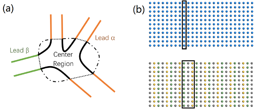
In the previous work by Sanvito and Lambert,RN80 the hopping matrix was required to be invertible. Here we expand to non-invertible . Suppose the primitive cell can be divided into layers, and the hopping matrix between every adjacent layers is invertible [see Fig.1(b)]. The modified method can apply in this situation even if the whole between two adjacent primitive cell is not invertible. In this case, the matrix in Eq.(3) can be substitute by
| (4) |
where and are the Hamiltonian of the -th layer and the hopping Hamiltonian between the -th and -th layers. Here all the are invertible, although is non-invertible. is the wavefunction at the -th layer in the cell . Substitute Eq.(4) and Bloch-wave into Eq.(3), we have:
| (5) |
and an equation of Bloch vector is acquired:
| (6) |
This is a rational expression equation of whose highest order is and lowest order is , so there are roots in total, where is the number of atoms in each layer as well as the dimension of each matrix block. Moreover, the hermiticity of this matrix guarantees that if vector satisfies the equation, satisfies as well. This results in a balance between leftward states and rightward states which can be seen if an infinitesimal imaginary number is added on the eigenenergy : According to relation , those leftward () hold a positive infinitesimal imaginary part, while the rightward () hold a negative one. For this reason, every leftward mode, both evanescent (whose hold a positive finite imaginary part) and transporting (whose hold a positive infinitesimal imaginary part) have its conjugate rightward counterpart.
In order to acquire all possible wavevectors and wavefunctions in Eq.(5), the transition matrix is introduced.
| (7) |
It can be simply deduced from Eq.(3) and Eq.(4) that
| (8) |
The transition matrix is defined as , thus we get
| (9) |
On the one hand, Eq.(9) shares the same solution and with Eq.(5). On the other hand, Eq.(9) is a eigenvalue equation, and the eigenvalues and eigenfunctions can be easily solved. As we have analyzed before, with a infinitesimal imaginary number added on the eigenenergy , have eigenvalues that indicating leftward wave vectors and corresponding rightward with . The transporting modes can be distinguished from those evanescent modes, because for transporting modes , while for evanescent modes hold a certain deviation from 1. Sort all eigenfunctions into a matrix by the ascending order of , we have
| (10) |
() is a diagonal matrix, whose diagonal is arranged by the ascending order of all . The wavefunctions () of all modes exist in corresponding matrixes and :
| (11) |
and
| (12) |
After solving the wavefunctions () and wavevectors (), the surface Green’s function of the lead can be obtained straightforwardly. Suppose the lead is leftward infinite and truncate at the -th layer of cell , the surface Green’s function is:
| (13) |
where
| (14) |
Next, we solve the transmission amplitude and reflection amplitude with the help of non-equilibrium Green’s function. The Green’s function have been obtained in previous references.bookadd The Green’s function of the whole system is defined from the equation, . Notice that the scattering state in Eq.(2) satisfies the Schrödinger equation , which is similar with the definition of except at and . So we can structure the Green’s function by using the scattering state :
| (15) |
Here we explain some denotes in Eq.(15). indicates the field layer in Green’s function, where denotes the primitive cell and denotes the layer in cell, and indicates the source layer. The source layer is fixed in the incident lead . Here , , , , , and the reflection amplitude all are the matrix with the dimension , the transmission amplitude is a matrix with the dimension . is a diagonal matrix of velocity , which can be acquired by
| (16) |
and is its rightward counterpart.
From Eq.(15), taking at the lead , the transmission amplitude matrix can be deduced:
| (17) |
Taking at the lead , the reflection amplitude matrix can be obtained:
| (18) |
Technically, evanescent modes which hold a complex velocity can be replaced by a in matrix and , ensuring that only transporting modes remain. After obtaining the transmission and reflection amplitudes, the transmission and reflection coefficients and .
Compare Eq.(2) and (15), the scattering wavefunction in the whole system can be obtained also,
| (19) |
where is required to be larger than . The matrix can be written as:
| (20) |
and is the scattering wavefunction in the whole system (including the center scattering region) for the incident electron from the lead at the mode . After obtaining the scattering wavefunction, the current density for a specific incident mode can be solved straightforwardly.
III Results and Discussions
In this section, we employ the above method to investigate modes mixing in graphene PNP junction. This is a two terminal system and the center scattering region is a PNP junction as shown in Fig.2. The Hamiltonian of graphene PNP junction can be written:
| (21) |
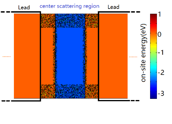
where () annihilates (creates) an electron on carbon atom , and are the nearest and second-nearest neighbor hopping energies. In this paper eV and . The magnetic factor comes from Peierls substitution and where is magnetic vector potential and .RN81 The on-site energy can be controlled by gate voltage, and is disorder potential. We set in the left and right P regions due to a global gate which can control them in the experiment, and in the center N region which can experimentally be tuned by a local gate. We take the disorder term where denotes the disorder strength and is a random factor drawn from the standard normal distribution. This is a short-range disorder and we will apply this type of disorder through out this paper except in Fig.5(c) and Fig.5(d) where we are discussing the effect of long-range disorder. The simulated disorder distribution is shown in Fig.2. Instead of adding disorder on the whole PNP region, disorder is added only near the boundary of nanoribbon and the interfaces of PN junctions (see Fig.2), where the wavefunction amplitude is most significant. In addition, if disorder exists in the middle of nanoribbon, it would leads the scattering among edge states on the upper and lower sides of the nanoribbon, which is significant in the simulated small system but strongly depressed in the experiment large device. The Green’s function of the whole system can be calculated from , with the Hamiltonian of the center scattering region. Here the center scattering region includes the center N region and parts of the left and right P regions. The retarded self-energy , where is the hopping Hamiltonian between the center region and the left/right leads and is the surface Green’s functions which can be calculated numerically from Eq.(13). Our following researches are made in armchair graphene nanoribbon, whose primitive cell contain 2 layers. The results are almost same for the zigzag ribbon.
In ballistic regime, when different modes completely mix-up, the conductance of PNP device is given asRN152
| (22) |
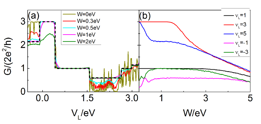
where refer to the filling factor in the center N region and left/right P region, and the factor 2 comes from spin degeneracy. A numerical simulation of a 170 layers armchair PNP device is performed in this section. The PNP device is consisted of a 70 layers center N region and the 50 layers left/right P region, and each layer contains 200 atoms. Except where noted, this device is exerted in a strong vertical magnetic field whose magnet index is for a hexagonal lattice, and the on-site energy in left/right P region is fixed to eV, corresponding to filling factor with Fermi energy eV. In the numerical calculation, all curves are averaged over up to 1000 random configurations.
Fig.3(a) depicts the conductance versus on-site energy with different disorder strengths , while the ideal conductance plateaus described by Eq.(22) is given as black dashed line. At eV, the conductance oscillates in bipolar regime, which consist with experimental result.reply1 The conductance plateaus emerge in the numerical simulation for the disorder strength about from 0.5eV to 1.5eV, and these plateau values are well consistent with the theoretical predictions and experimental results.RN152 This is clearer in Fig.2(b) which show the conductance vs , that every plot presents a plateaus, which is exactly theoretical value. In unipolar regime (e.g. , and ), the conductance is large at the perfect PNP junction (). In bipolar regime (that and ), is small at and raises with disorder in weak strength , indicating a promotion to transport resulted from mode mixing. Then the plateaus emerge at medium . The plateaus for the lowest filling factor (e.g. and ) can keep in a very large range of , and the plateaus for higher filling factors are slightly narrow. All plateaus are succeeded by an decline regime, because the system enters the insulator regime at strong .
In order to show mode mixing process specifically, a detailed inspection is taken on the effect of disorder at different filling factor . In the following context, (a,b,a) PNP junction symbolize a graphene PNP junction with and . We perform numerical simulation on (3,5,3), (3,1,3), and (3,-1,3) PNP junctions in sequence, corresponding to three different situation in Eq.(22). All parameters are the same as in Fig.3, except for on-site energy of the center N region and the disorder strength .
At , the system is a (3,5,3) unipolar PNP junction. Because that there are three incident modes in the left P terminal and three outgoing modes in the right P terminal, the transmission and reflection coefficient matrixes and have elements, and they as a function of the disorder strength are shown in Fig.4. In a perfect graphene device that eV, the transmission matrix elements , and are close to 1. Other six elements of the transmission coefficient matrix and all nine elements of the reflection coefficient matrix are close to 0. This indicates a high transparency of incident waves in perfect (3,5,3) PNP junction. There is no mode mixing and the incident electron goes forward along the original mode through the PNP junction. With the increasing of disorder strength , , and reduce and other six elements of matrix increase, and they converge together at about eV. While larger than a critical disorder strength (about eV), nine elements of matrix are equal well. All nine elements of matrix also increase with the increasing of , and they are equal while larger than a critical disorder strength . The critical for matrix is equal to one of matrix, indicating transmission modes and reflection modes mix up at the same disorder strength. In particular, a plateau emerges in the curves - and - at about eVeV [see Fig.3(a) and 3(b)]. In this plateau, all nine transmission elements keep the same value and so do the nine reflection elements . For the unipolar junction with , their plateau value are
| (23) | |||||
| (24) |
For the (3,5,3) PNP junction with and , and . Notice that the same of all nine and indicates that an incident mode is either scattered into any one of three transmission modes in equal possibility, or into any one of three reflection modes in equal possibility, which clearly show the occurrence of the perfect mode mixing. While increases further, the system turn into the insulator regime, then all elements of matrix reduce and all elements of matrix increase. However, all elements of and matrixes keep same still.
Next, we consider the effect of the magnetic field on the mode mixing. Fig.5(a) and (b) show the nine elements of transmission coefficient matrix in a (3,5,3) unipolar junction with the magnetic flux and , respectively. The similar results can be obtained. In a clean PNP junction that , , and have a large value with close to 1, and other six elements of matrix are small. At a critical disorder strength , all nine elements of matrix converge together and they are equal well while . These results clearly show the occurrence of the perfect mode mixing while . The critical disorder strength eV under and eV under . Together with the value eV under in Fig.4, it comes to the conclusion that the critical disorder strength slightly decreases with the increase of the intensity of the magnetic field. The larger magnetic field is, the slower decrease is. These features can be qualitatively explained with the help of the cyclotron radius of the magnetic field. The large magnetic field makes the electron trajectory closer to the interfaces of the PNP junction and the boundary of the graphene nanoribbon, and then the edge modes overlap together in space. So it is easy that the perfect mode mixing occurs.
Up to now, we only consider the short-range disorder. In this paragraph, let us investigate the mode mixing under long-range disorder. The strength of short-range and long-range disorders can not be simply compared. In order to make them more comparable, for the long-range disorder case, we choose the form of the disorder term in the Hamiltonian [see Eq.(21)] as:disorder
| (25) |
where is the spatial correlation parameter, is the distance between carbon atoms and , and with the disorder strength and the standard normal distribution . The normalization coefficient is chosen as
| (26) |
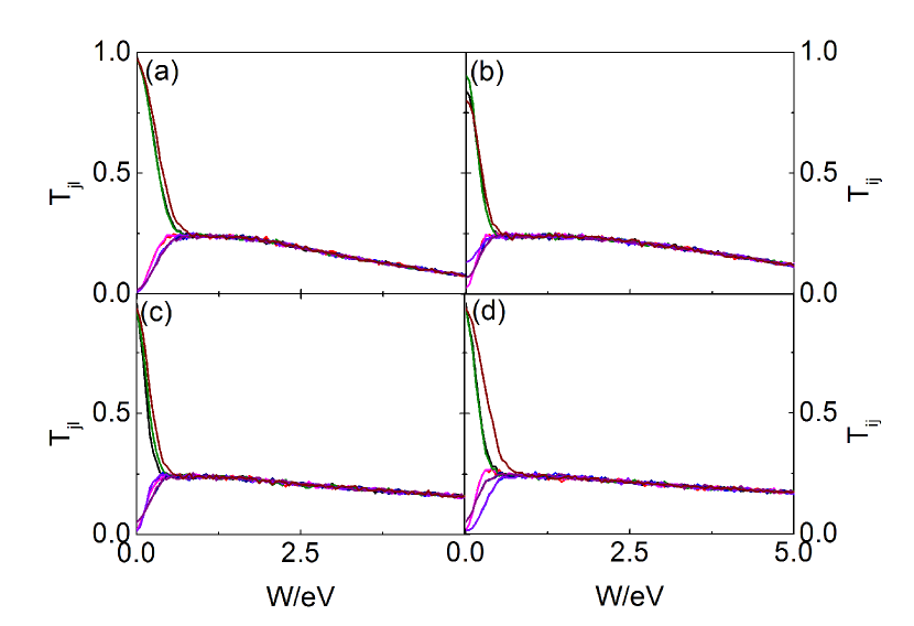
The sum in Eq.(26) is taken over a infinite graphene plane. Using this normalization, the variance of on-site energy is equal in short-rang and long-range disorders for a infinite graphene plane. Mode mixing procedure with long-range disorder is presented in Fig.5(c) and (d). For all the range , nine elements of matrix can converge together well while the disorder strength larger a critical disorder strength. This means that the perfect mode mixing can occur regardless of the short-range and long-range disorders. With the increase of the range , the convergence of transmission coefficient is significantly slower than other coefficients. This indicates the robustness of the first edge mode and it is difficult to mix the first edge mode with others. From Fig.6(a), (b) and (c), we can see that the first mode is closest to the boundary. On the other hand, under the long-range disorder, the disorder potential approximatively keeps it in the range . So it needs a larger disorder strength to mix the first mode with others, in particular, for the large value .

In the following, we take the magnetic flux under the short-range disorder again. Fig.6(a)-(l) show the space distribution of wavefunction and the current density for all three incident modes from the left lead at the (3,5,3) PNP junction, respectively. For the perfect graphene PNP junction with eV, and for the first incident mode mainly distributes at the region very close to the lower boundary of the device and they almost are zero at other region [see Fig.6(a) and (d)], because that the first mode is the edge state of the first Landau level and it is very close to the boundary. For the second and third incident modes, the wavefunction slightly emerges at the interface of the PNP junction [see Fig.6(b) and (c)], but the reflection wavefunction and the reflection current density are very small still. These results clearly show the incident electron goes forward along the original mode through the perfect (3,5,3) PNP junction and the mode mixing does not occur. On the other hand, while in the presence of the disorder (eV) the mode mixing occurs, all the three scattering states show much similarity. From Fig.6(g), (h) and (i), one can clearly see that the wavefunction distributions in the center regions for the three incident modes are almost the same. In addition, the current density for all three incident modes are same also [see Fig.6(j)-(l)]. This means that the perfect mode mixing not only makes that the incident electron has the equal probability to each outgoing (reflection) modes, but also makes the same current density in whole scattering region for all incident mode.
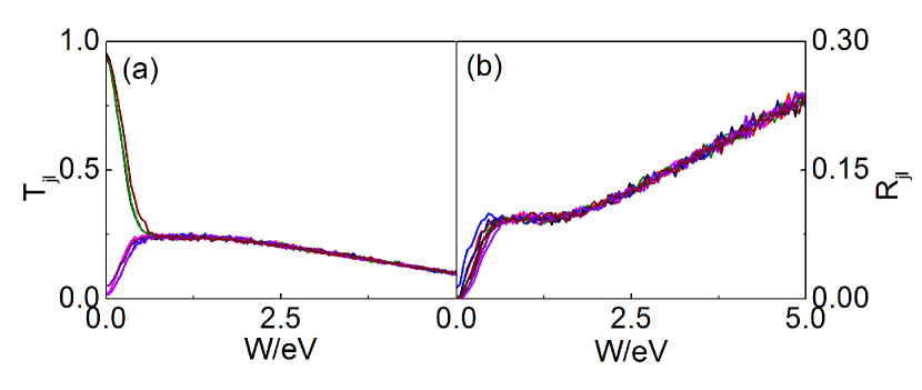
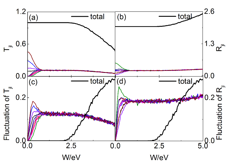
Next, let us study the (3,1,3) unipolar PNP junction. Since there is only one conducting mode in the center N region which is less than three modes in the left and right P regions, the conductance is decided by the filling factor of the center region. In this case, some works have shown that the mode mixing is absent and the conductance is usually , except for in the insulator regime while at the very strong disorder . Fig.6(a) and (b) show the 9 elements of the transmission and reflection coefficient matrixes as well the total transmission and reflection coefficients versus the disorder strength . The total transmission coefficient is 1 and the total reflection coefficient is 2 in a large range of (from to eV), as expected. From the results of the total and , it shows that the carrier seem to flow ballistically through the PNP junction and the mode mixing seem to be unimportant. However, from the 9 elements of and , they clearly show the occurrence of the mode mixing still. At the absence of the disorder (eV), the is very large and other 8 elements are very small [see Fig.6(a)], which means that the incident electron from the first mode can well go forward along the same mode through the junction and the incident electron from other mode is reflected back. With the increase of , the reduces and other 8 elements increase due to the mode mixing, although the total keeps 1 still. They converge together at about eV. Then while eV, all elements and are same. While in the range of from eV to eV, and show the plateau with and . These results clearly show the occurrence of the perfect mode mixing while eVeV.
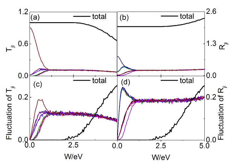
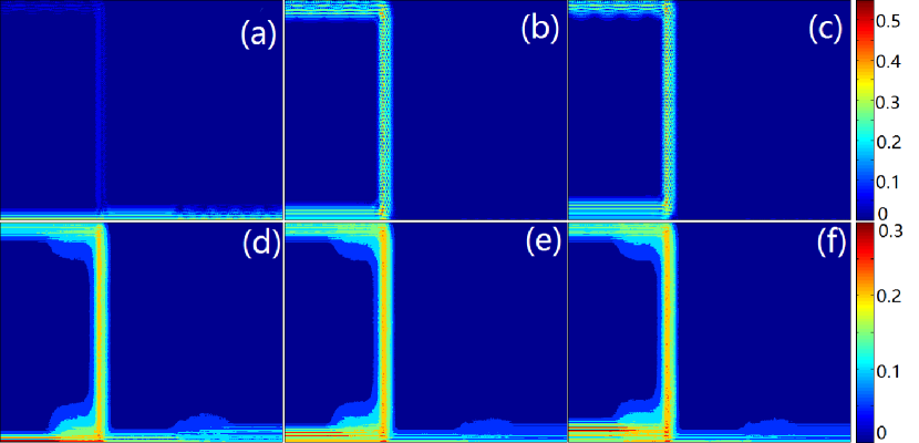
Fig.6(c) and (d) shows the fluctuation of the each element and total of the transmission and reflection coefficients for the (3,1,3) PNP junction. Here the fluctuation is defined as, e.g. and is the average over the random disorder configurations. The fluctuations of the total transmission efficient and total reflection efficient are zero while less than eV, this seem to show the ballistical transport and the mode mixing is absent. However, all elements of transmission and reflection matrixes hold a nonzero fluctuation, although the sum of them has a zero fluctuation. This clearly indicates the occurrence of the mode mixing. In particular, at the perfect mode mixing case, the 9 elements of and have the same fluctuations. They exhibit the plateau while eVeV. For the (3,1,3) PNP junction, the plateau value of fluctuation of is and the plateau value of fluctuation of is .
The space distributions of wavefunction for three incident modes in the (3,1,3) PNP junction are shown in Fig.7. At the disorder strength eV, three scattering states are very different [see Fig.7(a)-(c)]. For the first incident mode, the wavefunction mainly distributes on the lower boundary, and it exhibits that this incident electron goes forward without backscattering. But for the second and third modes, the incident electrons are mainly backscattered along the upper boundary. On the other hand, while eV, three scattering states show well similarity [see Fig.7(d)-(f)], this indicates the occurrence of the perfect mode mixing, although the total transmission coefficient is 1 still.
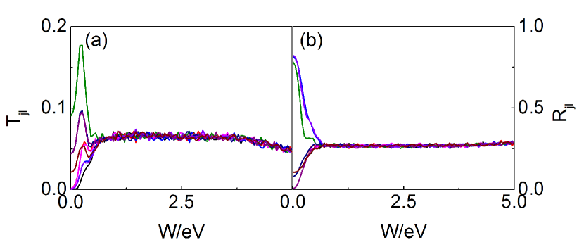
Bipolar PNP junction is formed by two PN junctions arranged back to back. Unlike in unipolar PNP junction where exists conducting channel and has a large conductance at eV, in bipolar PNP junction PN interfaces block the conducting channel and the conductance usually is small at the absence of the disorder [see Fig.3]. In bipolar junction, disorder can promote electron transport and increase the conductance due to mode mixing.RN61 ; RN150 This can be seen in Fig.3(b) where the conductances of and raise in weak disorder case. Fig.9 shows the 9 elements of the transmission and reflection coefficient matrixes versus disorder strength for the (3,-1,3) bipolar PNP junction. At weak , the 9 elements of and matrixes are very different. However, about at eV, all 9 elements of () matrixes well merge together. They are equal always for the larger , and they exhibit the plateaus at the large range of eVeV, which well indicates perfect mode mixing for eV. The plateau values are and . For the (3,-1,3) junction with and , and , which is well consistent with the numerical results in Fig.9(a) and (b).
All these aforementioned numerical simulations are based on the armchair nanoribbon. We have also performed these numerical calculations in the PNP junction based on the zigzag nanoribbon, whose size matches the simulated armchair one, that means the simulated zigzag nanoribbon is also consisted of a 70 layers center N region and two 50 layers left and right P regions, and each layer contains 200 atoms. We have repeated all curves in Fig.3-9, and obtained the same results.
In addition, this method can be applied in other materials. We choose a edge-reconstructed zigzag PNP junction for example. Its boundary is reformed by Stone-Wales defects, that pentagon-heptagon pairs which often forms at the boundary of CVD-grown graphene.RN82 Fig.10 presents the transmission and reflection coefficient matrixes as well as their fluctuation versus disorder strength . The results are very similar with the armchair nanoribbon case (see Fig.7 and 10). The total transmission and reflection coefficients display the plateau beginning at eV to eV. But the 9 elements and are not equal at . They merge until eV and then show the plateau for from eV to eV. While at the plateau, the fluctuation of the total transmission and reflection coefficients are exactly zero. However, the fluctuation of the 9 elements and are not zero, and they exhibit the plateau with the plateau values for and for . These indicate the occurrence of perfect mode mixing which are quite similar to the armchair PNP junction case.
IV Conclusions
In summary, we have obtained an extended transmission and reflection coefficient formulas in two-terminal system by Sanvito and Lambert to the multi-terminal system. These formulas can give the scattering wavefunction and the current density in the real space for a specific incident mode from an arbitrary terminal, as well as can give the transmission and reflection coefficients from a specific incident mode to an arbitrary outgoing mode. By using these formulas, we study electron transport through a graphene PNP junction. While at the perfect PNP junction, the elements of the transmission and reflection coefficient matrixes are very different, and the space distribution of the scattering wavefunction for different incident modes have large difference as well. But they merge at the presence of disorder. While the disorder is stronger than a critical value, all elements of the transmission matrix are same regardless of unipolar or bipolar junctions, so are all elements of the reflection matrix. At the suitable disorder, all elements of the transmission and reflection matrixes show the plateau structure, as well the scattering wavefunction for the different incident modes are similar. These results clearly indicate the occurrence of perfect mode mixing. Moreover, the perfect mode mixing can occur regardless of the intensity of the magnetic field and the disorder nature. In particular, while the mode number in the center region is less than that in the left and right regions in the unipolar PNP junction, an interesting phenomenon occurs. Here the fluctuation of the total transmission and reflection coefficients are exactly zero, which seem to indicate the ballistic transport. However, all elements of transmission and reflection matrixes show the fluctuation and clearly mean the occurrence of the perfect mode mixing in this case also.
Acknowledgments
We gratefully acknowledge the financial support from NBRP of China (2015CB921102), NSF-China under Grants No. 11274364 and 11574007.
References
- (1) P. R. Wallace, Phys. Rev. 71, 622 (1947).
- (2) A. H. Castro Neto, F. Guinea, N. M. R. Peres, K. S. Novoselov, and A. K. Geim, Rev. Mod. Phys. 81, 109 (2009).
- (3) M. I. Katsnelson, K. S. Novoselov, and A. K. Geim, Nature Phys. 2, 620 (2006).
- (4) K. S. Novoselov, V. I. Fal’ko, L. Colombo, P. R. Gellert, M. G. Schwab, and K. Kim, Nature 490, 192 (2012).
- (5) A. Cresti, Nanotechnology 19, 265401 (2008).
- (6) J. R. Williams, L. DiCarlo, and C. M. Marcus, Science 317, 638 (2007).
- (7) F. Schwierz, Nature Nanotech. 5, 487 (2010).
- (8) C.-H. Kim and C. D. Frisbie, J. Phys. Chem. C 118, 21160 (2014).
- (9) J.-T. Liu, J.-H. Huang, W.-B. Xiao, A.-R. Hu, and J.-H. Wang, Acta Phys. Sinica 61, 177202 (2012).
- (10) Y. M. Lin, A. Valdes-Garcia, S. J. Han, D. B. Farmer, I. Meric, Y. N. Sun, Y. Q. Wu, C. Dimitrakopoulos, A. Grill, P. Avouris, and K. A. Jenkins, Science 332, 1294 (2011).
- (11) N. N. Klimov, S. T. Le, J. Yan, P. Agnihotri, E. Comfort, J. U. Lee, D. B. Newell, and C. A. Richter, Phys. Rev. B 92, 241301 (2015).
- (12) S. Nakaharai, J. R. Williams, and C. M. Marcus, Phys. Rev. Lett. 107, 036602 (2011).
- (13) V. V. Cheianov, V. Fal’ko, and B. L. Altshuler, Science 315, 1252 (2007).
- (14) V. V. Cheianov and V. I. Fal’ko, Phys. Rev. B 74, 041403 (2006).
- (15) J. R. Williams and C. M. Marcus, Phys. Rev. Lett. 107, 046602 (2011).
- (16) J.-C. Chen, X. C. Xie, and Q.-F. Sun, Phys. Rev. B 86, 035429 (2012).
- (17) Y. Liu, R. P. Tiwari, M. Brada, C. Bruder, F. V. Kusmartsev, and E. J. Mele, Phys. Rev. B 92, 235438 (2015).
- (18) P. Rickhaus, P. Makk, M.-H. Liu, E. Tóvári, M. Weiss, R. Maurand, K. Richter, and C. Schöenenberger, Nat. Commun. 6, 6470 (2015).
- (19) T. Taychatanapat, J. Y. Tan, Y. Yeo, K. Watanabe, T. Taniguchi, and B. Özyilmaz, Nat. Commun. 6, 6093 (2015).
- (20) F. Amet, J. R. Williams, K. Watanabe, T. Taniguchi, and D. Goldhaber-Gordon, Phys. Rev. Lett. 112, 196601 (2014).
- (21) F. Amet, J. R. Williams, K. Watanabe, T. Taniguchi, and D. Goldhaber-Gordon, Phys. Rev. Lett. 110, 216601 (2013).
- (22) J. Velasco, Y. Lee, L. Jing, G. Liu, W. Bao, and C. N. Lau, Solid State Commun. 152, 1301 (2012).
- (23) J. Velasco, G. Liu, W. Z. Bao, and C. N. Lau, New J. Phys. 11, 095008 (2009).
- (24) M. F. Craciun, S. Russo, M. Yamamoto, and S. Tarucha, Nano Today 6, 42 (2011).
- (25) S.-G. Nam, D.-K. Ki, J. W. Park, Y. Kim, J. S. Kim, and H.-J. Lee, Nanotechnology 22, 415203 (2011).
- (26) D.-K. Ki, S.-G. Nam, H.-J. Lee, and B. Özyilmaz, Phys. Rev. B 81, 033301 (2010).
- (27) J. Baringhaus, A. Stöhr, S. Forti, U. Starke, and C. Tegenkamp, Sci. Rep. 5, 9955 (2015).
- (28) H. Liu, Y. Liu, and D. Zhu, J. MATER. CHEM. 21, 3335 (2011).
- (29) E. C. Peters, E. J. H. Lee, M. Burghard, and K. Kern, Appl. Phys. Lett. 97, 193102 (2010).
- (30) A. F. Young and P. Kim, Nature Phys. 5, 222 (2009).
- (31) Y. Xing, J. Wang, and Q.-F. Sun, Phys. Rev. B 81, 165425 (2010).
- (32) T. Low, Phys. Rev. B 80, 205423 (2009).
- (33) D. A. Abanin and L. S. Levitov, Science 317, 641 (2007).
- (34) W. Long, Q.-F. Sun, and J. Wang, Phys. Rev. Lett. 101, 166806 (2008).
- (35) B. Özyilmaz, P. Jarillo-Herrero, D. Efetov, D. A. Abanin, L. S. Levitov, and P. Kim, Phys. Rev. Lett. 99, 166804 (2007).
- (36) J. Velasco, G. Liu, L. Jing, P. Kratz, H. Zhang, W. Bao, M. Bockrath, and C. N. Lau, Phys. Rev. B 81, 121407 (2010).
- (37) G. Liu, J. Velasco, Jr., W. Bao, and C. N. Lau, Appl. Phys. Lett. 92, 203103 (2008).
- (38) S. Morikawa, S. Masubuchi, R. Moriya, K. Watanabe, T. Taniguchi, and T. Machida, Appl. Phys. Lett. 106, 183101 (2015).
- (39) N. Kumada, F. D. Parmentier, H. Hibino, D. C. Glattli, and P. Roulleau, Nat. Commun. 6, 8068 (2015).
- (40) S. Matsuo, S. Takeshita, T. Tanaka, S. Nakaharai, K. Tsukagoshi, T. Moriyama, T. Ono, and K. Kobayashi, Nat. Commun. 6, 8066 (2015).
- (41) J.-C. Chen, T. C. Au Yeung, and Q.-F. Sun, Phys. Rev. B 81, 245417 (2010).
- (42) J. Li and S.-Q. Shen, Phys. Rev. B 78, 205308 (2008).
- (43) S. Sanvito, C. J. Lambert, J. H. Jefferson, and A. M. Bratkovsky, Phys. Rev. B 59, 11936 (1999).
- (44) R. Landauer, IBM J. Res. Dev. 1, 223 (1957).
- (45) S. Datta, Electronic Transport in Mesoscopic Systems (Cambridge university press, 1997).
- (46) R. Peierls, Z. Phys. 80, 763 (1933).
- (47) S.-G. Cheng, H. Zhang, and Q.-F. Sun, Phys. Rev. B 83, 235403 (2011).
- (48) H. Schmidt, J. C. Rode, C. Belke, D. Smirnov, and R. J. Haug, Phys. Rev. B 88, 075418 (2013).
- (49) J. N. B. Rodrigues, P. A. D. Goncalves, N. F. G. Rodrigues, R. M. Ribeiro, J. M. B. Lopes dos Santos, and N. M. R. Peres, Phys. Rev. B 84, 155435 (2011).