Generalized Fowler-Nordheim field-induced vertical electron emission model for two-dimensional materials
Abstract
Current theoretical description of field-induced electron emission remains mostly bounded by the classic Fowler-Nordheim (FN) framework developed nearly one century ago. For the emerging class of two-dimensional (2D) materials, many basic assumptions of FN model become invalid due to their reduced dimensionality and exotic electronic properties. In this work, we develop analytical and semi-analytical models of field-induced vertical electron emission from the surface of 2D materials by explicitly taking into account the reduced dimensionality, non-parabolic energy spectrum, non-conserving in-plane electron momentum, finite-temperature and space-charge-limited effects. We show that the traditional FN law is no longer valid for 2D materials. The modified vertical field emission model developed here provides better agreement with experimental results. Intriguingly, a new high-field regime of saturated surface field emission emerges due to the reduced dimensionality of 2D materials. A remarkable consequence of this saturated field emission effect is the absence of space-charge-limited current normally expected at high field in three-dimensional bulk material.
I Introduction
The formulation of electron emission theory based on Sommerfeld’s free electron model of metals sommerfeld represent one of the earliest successes of quantum mechanics in solid state physics hoddeson . The thermionic emission (TE) of hot electrons above the surface potential barrier and the sub-barrier quantum mechanical tunnelling of cold electron via field emission (FE) are governed, respectively, by the Richardson-Dushman (RD) RD and the Fowler-Nordheim (FN) laws FN ,
| (1a) | |||
| (1b) |
where , , , , and are the work function, temperature, electric field strength, Richardson constant, the first and the second FN constants, respectively emission_const .
The RD and the FN laws follow a remarkable symmetry – both are composed of a material-dependent pre-factor multiplied by a universal exponential factor of for TE and for FE. The exponential terms provide tell-tale signatures of the underlying emission mechanism since the - and the - characteristics are almost exclusively determined by temperature and electric field. Thus, Eq. (1) is extraordinarily versatile and can be nearly universally applied to analyse the electron emission characteristics for a wide range of materials by using the Arrhenius plot: versus for TE or the FN plot: versus for FE. Nonetheless, much of the material-dependent physics contained in the pre-factor remains obscured in the experimental data when analysed using Eq. (1). This poses a potential danger of misinterpreting the emission physics in unconventional materials especially when their physical properties do not permit the use of Eq. (1).
Although the classic RD and FN models for bulk materials have been continually refined over past decades p_zhang ; TF ; MG ; burgess ; stratton ; forbes ; forbes2 ; forbes3 ; forbes4 ; jensen ; jensen2 ; jensen3 ; kyritsakis ; sd_liang ; wei ; wei2 ; edgcombe ; holgate , their validity for the emerging class of two-dimensional (2D) materials have been questioned recently liang ; sinha ; ang ; IEDM2016 ; misra ; misra2 ; liang2 . Based on a continuum emission picture, Liang and Ang have shown that graphene thermionic emitter exhibits unconventional scaling in the pre-factor liang ; liang2 . The Liang-Ang continuum model is generalized to the case of narrow-gap semiconductor and few-layer graphene by Ang and Ang ang . To model the charge transport across a graphene-based Schottky contact, Sinha and Lee adopted an alternative ‘time’-constant-based TE model sinha , which contains a polynomial pre-factor of and an empirical ‘time’-like parameter, , in the emission current density. Albeit the very different underlying physical pictures, both Liang-Ang and Sinha-Lee TE models agree reasonably well with experiments sinha ; IEDM2016 ; massicotte .
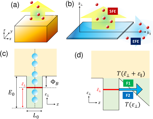
Despite significant progress in the theoretical development of TE, cold electron FE theory remains relatively less-explored MRS . For traditional bulk material, FE does not sensitively rely on the direction of emission for materials with isotropic energy dispersion [Fig. 1(a)]. In contrast, the thin-film nature of 2D materials breaks the symmetry of emission configuration and leads to two distinct subtypes: (i) edge field emission (EFE) where electrons are emitted along the 2D plane; and (ii) surface field emission (SFE) where electrons are emitted normally from the 2D-plane [see Fig. 1(b)]. In EFE wang_edge ; kumar ; moussa ; xu ; wu_GVT ; sun ; song ; carbon , the electrons has a continuous in-plane energy dispersion component along the emission direction while in SFE, the electron dynamics along the emission direction is quantized due to the quantum confinement by surface potential rz_wang ; wei3 . Nonetheless, the traditional FN law is employed in the vast majority of graphene FE experiments malesevic ; eda ; qian ; wu ; huang ; yamaguchi ; santandrea ; wang_edge ; kumar ; palnitka ; soin ; kleshch ; moussa ; xu ; wu_SFE ; yusop ; bartolomeo ; Iemmo albeit the fact that the underlying FE mechanism in 2D material differs significantly from the bulk counterpart. Modified EFE theory based on a 2D emitter model is proposed qin and verified experimentally xiao to exhibit an unconventional -scaling in the prefactor. Such EFE model is further refined by Wang et al to include the geometrical edge effect and the relativistic energy dispersion of graphene wang .
Thus far, the physical model underlying SFE from 2D materials remains incomplete. In this work, we develop analytical and semi-analytical models of field-induced vertical electron emission from the surface of 2D materials by explicitly taking into account their reduced dimensionality, non-parabolic energy spectrum, non-conservation of lateral momentum (i.e. momentum component lying in the plane of 2D material), finite-temperature and space-charge-limited effects. Our model exhibits a significant departure from the traditional FN law, thus signaling the breaks down of FN paradigm in 2D materials. From our model, an unconventional - scaling relation is found, i.e.
| (2) |
Here, the pre-factor is -independent, rather than the -dependence in the traditional FN law [see Eq. (1b)]. Correspondingly, the FN-plot is modified as: versus , which is shown to provide a better agreement with experimental data (see Fig. 4 below). Intriguingly, the reduced dimensionality of 2D materials bestows a new regime of saturated surface field emission at high electric field.
For FE from 3D bulk materials, when its current density is sufficiently large, the built-up of space charge in the vacuum gap can lead to a transition from field-induced quantum mechanical tunneling to space-charge-limited (SCL) flow barbour ; lau ; kelvin2 ; forbes_trans ; p_zhang2 , where the latter is governed by the Child-Langmuir (CL) law CL . The solid-state counter part of SCL effect in 2D Dirac semiconductor has been recently reported to exhibit an unconventional current-voltage scaling relation ang_DiracSCLC . For 2D material field emitter, the following questions arise: can the emission current from 2D materials evolve from field emission to semiclassical SCL flow? Thus far, this question has not been studied both theoretically or experimentally yet. Here we address this question by constructing a general emission model – covering both FE and SCL regimes – through the combination of 2D material FE models and 1D Poisson equation lau . We show that the dimensionality-induced saturated emission results in a remarkable consequence: the space-charge-limited flow of electrons can be fully eliminated in 2D-material-based surface field emitter at nanometer and micrometer scales with practical range of applied voltage.
The saturated FE and the peculiar absence of space-charge effect shall have profound impacts on the characterization and design of 2D-material-based field emitter and vacuum nanoelectronics. Furthermore, as field-induced vertical electron emission from the 2D planar surface represents one of the central transport mechanisms in solid-state 2D-material-based electrical contact allain ; xu_rev ; bartolomeo2 ; jariwala , the models developed here shall provide a theoretical basis in the analysis of charge transport phenomena in such interfaces.
II Overview of electron emission formalism: From bulk to 2D materials
II.1 Electron emission from bulk material
The general form of the electrical current density can be written as
| (3) |
where , , , and are wavevector, carrier group velocity, transmission probabilities, carrier distribution function and total volume of the emission system, respectively. We partition the emitted electron energy and wavevector as followed:
| (4) |
where () is the energy component transversal to (along) the emission direction, and () is the wavevector component transversal to (along) the emission direction [see Fig. 1(b)]. For a three-dimensional (3D) bulk material, the emission current density can be written as
| (5) | |||||
where the density of states (DOS) in the plane lateral to the emission direction is defined as for an isotropic lateral energy dispersion and is the spin-valley degeneracy. In obtaining Eq. (5), we have taken the continuum limit of and re-written the group velocity along the emission direction as . For TE, the transmission probabilities are set to unity for and the carrier distribution function is approximated by semiclassical distribution,
| (6) |
For FE, the zero-temperature Fermi-Dirac distribution is employed and the transmission probabilities is calculated via the Wentzel-Kramers-Brillouin (WKB) approximation for triangular barrier, i.e.
| (7) |
where , , is the electron mass in free-space, is the electric field strength and emission_const . By combining Eqs. (5–II.1), we obtain the traditional RD and FN relations in Eq. (1). Note that in taking the transmission probability in the form of , it is implied that the lateral energy component, , does not contribute to the -directional tunneling, i.e. the lateral momentum component, , is strictly conserved. Thus, the classic RD and FN laws belong to the class of conversing lateral momentum (CLM) emission theories. As we shall see below, CLM can be relaxed in 2D materials and this leads to distinctive electron emission characteristics.
II.2 Electron emission from the surface of 2D material
The traditional FN law [see Eq. (1b) above] is derived based on the following assumptions: (i) in order to calculate the emission current density, both and are required to be continuously integrable; (ii) the is assumed to be parabolic in ; (iii) due to CLM, the transmission probability is a function of only, i.e. ; and (iv) the condition of for metallic bulk field emitter.
For 2D materials, all of the above assumptions become invalid. Firstly, due to the lack of crystal periodicity along the -direction, does not follow a continuous dispersion relation. Instead, the cross-plane dynamics is described by discrete bound state energy levels as the electrons are confined by the surface potential vega [see Fig. 1(c)]. In this case, the energy and wavevector partition rule in Eq. (II.1) should be replaced by:
| (8) |
where and denotes the discrete bound state energy and the quantized -directional wavevector, respectively. Secondly, the in-plane energy dispersion, , is non-parabolic in for many 2D materials such as graphene and few-layer transition metal dichalcogenide (TMD). Thirdly, for the out-of-plane tunnelling of 2D electron gas into 3D bulk material, the inevitable presence of electron-electron and electron-impurity scatterings leads to a non-conserving lateral momentum (NCLM) during the tunneling process meshkov . Such NCLM emission mechanism has been previously proposed as a route of enhancing thermionic cooling efficiency in semiconductor-based superlattice vashaee ; vashaee2 ; dwyer ; jeong . Recently, NCLM has been experimentally observed in the cross-plane interfacial charge transport TMD-based van der Waals heterostructure zhu . Under the NCLM framework, the transmission probability is modified into a function of total energy, , instead of , i.e. and its WKB form is written as meshkov
| (9) |
where is a parameter describing the strength of NCLM scattering processes, is a -dependent potential barrier and the emission occurs along the -direction. The actual value of varies depending on the quality of field emitter such as impurities and structural defects chen_NP . Furthermore, the substrates can also affect via the dielectric screening effect ando ; hwang ; ponomarenko . Therefore, the magnitude of the SFE current in 2D material field emitter is expected to vary significantly in samples of different qualities and/or substrate configurations. Using the experimental data of graphene-based Schottky contact sinha , we estimate for graphene electron emitter and this value is used throughout the following discussions (see Sec. V.A below for detailed discussion). Lastly, the assumption of is no longer warranted for zero-gap 2D materials such as graphene in which the can be electrostatically tuned from 0 to eV chen_FL , thus allowing the condition of or even .
The emission current density in 2D materials can be constructed by replacing the continuous -integral in Eq. (5) with a summation of all quantized bound states (), denoted as , below the surface potential, i.e.
| (10) | |||||
where the superscript and denotes CLM and NCLM models, respectively. The term is the cross-plane velocity. In Eqs. (10) and (II.2), the 2D material thickness, nm for graphene, arises from the discrete summation [see Eq. (3)]. For single layer graphene, the energy difference between the Dirac point and the vacuum level is reported as eV yu_wf ; xu_wf ; chris (Note that ). We thus assume that the SFE process is chiefly contributed by only one bound state level lying at eV below the vacuum level. This bound state energy, denoted as , is numerically solved from the time-independent Schrödinger’s equation using a finite square well model proposed by Vega and de Abajo vega [see Fig. 1(c)]. By matching the wavefunction maxima of the 2 orbital of graphene and fitting the bound state energy to below the vacuum level, the quantum well width, , is numerically calculated to be 0.12 nm vega2 and the quantum well depth is eV, which yields the bound state energy of eV [see Fig. 1(c) for energy band diagram]. We set this value of as the zero-reference of total energy, i.e thus allowing the emission current density to be simplified as
| (12a) | |||
| (12b) |
A key difference between CLM and NCLM models is that for , the can be factored out from the -integral since it is a function of solely while for , the remains implicit to the -integral [Fig. 1(d)].
III Theory of surface field emission from 2D materials
III.1 Lateral energy dispersion and density of states in 2D materials
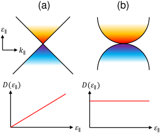
In the following, Eqs. (12b) and (12a) are solved for two major classes of , namely the non-relativistic parabolic energy dispersion of and the linear gapless Dirac energy dispersion of . The -linear energy dispersion describes the low energy electrons residing at the and Dirac cone of graphene monolayer neto . For Bernal-stacked bilayer graphene, the effective low energy dispersion around the and points follows the -parabolic energy dispersion mccann . The lateral DOS can be obtained as
| (13a) | |||
| (13b) |
respectively, for parabolic and linear dispersion of . Here, m/s is the Fermi velocity in monolayer graphene neto and li is the electron effective mass in Bernal-stacked bilayer graphene li . The linear and parabolic form of and are shown in Fig. 2.
For few-layer black phosphorus field emitter suryawanshi , the lateral energy dispersion near the conduction band edge can be approximated by an anisotropic-parabolic spectrum jiang ; han , i.e. , where , and is the conduction band electron effective mass in - and -directions, respectively. The lateral DOS follows the same form as the isotropic parabolic lateral DOS in Eq. (13), i.e. , where is the DOS electron effective mass and is the spin degeneracy. Thus, the FE models developed below can be readily generalized for few-layer black phosphorus field emitter by substituting and .
III.2 2D material field emission with conserving lateral momentum (CLM)
For SFE from 2D material with CLM, the WKB transmission probability is given as , where is defined in Eq. (II.1). By setting as the zero-reference of , i.e. and employing the K condition, Eq. (12a) can be solved as
| (14a) | |||
| (14b) |
respectively, for 2DEG and Dirac energy dispersions. Although both traditional FN law for bulk material and the modified FE model for 2D material in Eq. (14b) belong to the same CLM models, their pre-factor exhibits contrasting -dependence – the pre-factor in Eq. (14b) is -independent rather than the -dependence as in the case of traditional FN law for 3D bulk material. Accordingly, the FN-plot is modified to
| (15a) | |||
| (15b) |
This is in stark contrast to the traditional FN-plot of . Furthermore, the FE current density exhibits a Fermi level scaling of and . The FE current density vanishes as due to the depletion of electrons.
It is important to point out the following: due to the absence of -dependence in the pre-factor, the surface field emission current density from 2D material will saturate at high-field limit of when both and approaches unity. In this case, the saturated field emission current density is
| (16a) | |||
| (16b) |
where the subscript ‘’ denotes saturated emission. The -independent pre-factor in Eq. (14b) arises from the absence of -integral in the formulation of 2D material current density [see Eq. (12)]. Thus, this saturated surface field emission represents a direct consequence of the reduced dimensionality which can be used to probe the 2D nature of 2D-material-based field emitter.

III.3 2D material field emission with non-conserving lateral momentum (NCLM)
In the case of NCLM, the WKB transmission probability across a triangular surface can be written as a function of total energy meshkov , i.e. . At K, Eq.(12b) can be analytically solved as
| (17a) | |||||
| (17b) | |||||
In the low-field regime of (), Eq. (17) reduces to
| (18a) | |||||
| (18b) | |||||
where the pre-factor is linear in for both 2DEG and Dirac dispersions. Correspondingly, the FN-plot for NCLM model at low-field regime is modified as
| (19a) | |||
| (19b) |
In the high-field regime of , the FE current density becomes equivalent to Eq. (14b) apart from an additional factor of ,
| (20a) | |||
| (20b) |
The modified FN-plot for NCLM model thus follow the same relation as Eq. (15) at high-field regime. At the limit of very high applied electric field strength, the FE current densities for CLM and NCLM converge to the same saturated value given by
| (21a) | |||
| (21b) |
The modified FN-plot in Eq. (15) and the saturated emission current densities in Eqs. (16) and (21) are universal high-field features for both CLM and NCLM models. The convergence of NCLM into CLM models at can be explained as follow. When is sufficiently large, the electrons contributing to FE has a relatively small lateral energy component, , in comparison with . In this case, the NCLM transmission probability becomes nearly -independent, i.e. . As a result, the NCLM model [Eq. (17)] converges to the CLM model [Eq. (14b)].
III.4 Field emission characteristics of CLM and NCLM models and comparison with experiment
In Figs. 3(a) and (b), the FE characteristics of CLM and NCLM models are shown with eV. In Fig. 3(a), the required electric field strength to achieve A/cm2 of emission current density is typically V/nm and V/nm, respectively, for CLM and NCLM models. At high-field regime, the emission current densities gradually saturate. For graphene, the saturated emission current density is in the order of A/cm2 and A/cm2, respectively, for NCLM and CLM models, which is well below the breakdown current density experimentally determined in suspended graphene, i.e. A/cm2 gruber . Hence, single layer graphene may serve as a feasible platform to experimentally probe the saturated field emission effect. The traditional FN plot is shown in Fig. 3(b). Due to the strong dominance of the exponential term, , the FN plots can still be fitted by straight lines although the pre-factor of the revised FE model has a completely different -dependence in comparison with the traditional FN model. In Fig. 3(c), the -dependence of the emission current density is plotted with V/nm. The FE current densities increase monotonously as increases. At low , we have . The opposite case of is obtained at eV. This cross-over occurs since is approximately one order of higher than for both CLM and NCLM models [see Eqs. (14b) and (17)].
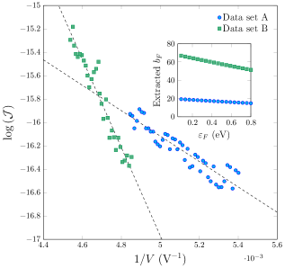
In Fig. 4, the high-field segments of the graphene SFE experimental data reported in Ref. xu is analysed using the proposed modified FN-plot in Eq. (15). Both modified FN-plot and the traditional FN plot produce reasonably good linear fit. Nonetheless, the coefficient of determination (COD), which quantifies the goodness of a linear fit (COD represents perfect straight line), is consistently improved for both sets of experimental data when fitted using the modified FN plot – the CODs are improved from 0.813 to 0.866 (Data set A in Fig. 4) and from 0.927 to 0.934 (Data set B in Fig. 4).
The field enhancement factor, , can be extracted from the modified FN-plot via
| (22) |
where is the energy difference between Dirac point (conduction band bottom) and vacuum level for linear (parabolic) lateral energy dispersion. is the slope extracted from the modified FN-plot. Here, we have assumed a simple field enhancement of where is the anode-cathode separation and is the applied voltage. Since the value of is not known, the extracted is plotted in the inset of Fig. 4 for a range of . For both sets of FE experimental data, is extracted. This low magnitude of field enhancement factor is consistent with the fact that sharp tips and edges are absent in graphene SFE configuration.
III.5 Finite-temperature surface field emission from 2D materials
We now generalized the SFE models for K. Because at K, we can safely neglect the TE effect. The finite-temperature CLM model of field emission from 2D materials can be straightforwardly solved as,
| (23a) | |||
| (23b) |
where is the first-order complete Fermi-Dirac integral abramowitz . For NCLM model, the finite-temperature model can be semi-analytically expressed in terms of generalized hypergeometric function abramowitz , where and are positive integers. We obtain,
| (24a) | |||||
| (24b) | |||||
where . Note that in deriving Eq. (24a), we have set the upper limit of -integral to to exclude the over-barrier thermionic emission. The terms and are given as functions of :
| (25) |
The temperature dependence of the NCLM model is not immediately obvious from the semi-analytical forms in Eqs. (24a) and (24b). To obtain simple analytical approximation of the NCLM model, we employ the Sommerfeld expansion foot_1 which is well-suited for the case of and . The finite temperature Sommerfeld correction to , i.e. , are
| (26a) | |||
| (26b) |
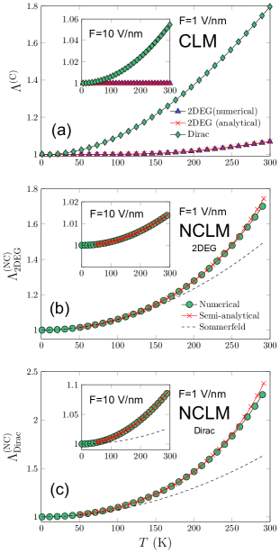
In Fig. 5, we plot the thermal-enhancement ratio, defined as
| (27) |
with V/nm (main plots) and with V/nm (insets). For both CLM and NCLM models, the thermal-enhancement of emission current is only profound at low-field regime. In Fig. 5(a), the numerical and semi-analytical results of and of CLM models are plotted. At V/nm, the room-temperature is thermally-enhanced by % with respect to [Fig. 5(a)]. This is in stark contrast to the modest thermal-enhancement of % at V/nm [inset of Fig 5(a)]. For parabolic energy dispersion, the thermal-enhancement of is less dramatic, i.e. % enhancement at V/nm and a nearly absence of thermal-enhancement at V/nm. The and of NCLM models are shown, respectively, in Figs. 5(b) and (c). The exhibit a similar thermal-enhancement of 80% at V/nm [Fig. 5(b)], but is suppressed to only % at V/nm [inset Fig. 5(b)]. For , a dramatic thermal-enhancement of % at room temperature is obtained with V/nm [Fig. 5(c)] and is reduced to % at V/nm [inset of Fig. 5(c)].
The room-temperature ( K) FE current densities can be ranked, respectively for V/nm and for V/nm, as
| (28a) | |||
| (28b) |
Note that the semi-analytical solution based on hypergeometric functions is in good agreement with the full numerical result. Also, the thermal-enhancement predicted by the Sommerfeld expansion in Eq. (26) agrees well with the semi-analytical model up to K. The contrasting thermal-enhancement of FE current at low- and at high-field regimes can be qualitatively explained by the Sommerfeld expansion in Eq. (26). As both and are proportional to , the thermal-enhancement becomes severely quenched at elevated electric field strength.
IV Absence of space-charge-limited emission in 2D material field emitter
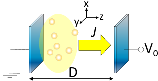
We now construct a general emission model – covering both FE and SCL regims – through the combination of FE models developed above and Poisson equation lau . We consider a planar vacuum diode composed of two large area 2D-material-based electrodes as shown in Fig. 6. We neglect the quantum SCL effect lau_QSCLC ; ang_QSCLC ; koh which is significant in nanoscale vacuum gap when the electrode-separation is comparable to the de Broglie wavelength of the emitted electrons. We further neglect finite-temperature effect since it produces only a small correction to the emission current densities at high electric field regime as discussed above. The electrostatic field distribution within the vacuum gap can be described by a 1D Poisson equation, , where the emission current density is . The electron is emitted along the -direction. Here, is the permittivity of free space and is the space charge density in the vacuum gap. By a change of variable, , and the definition of , the Poisson equation can be transformed into the Llewellyn form lau ,
| (29) |
where the -argument of is suppressed for simplicity. Integrating both sides with respect to once and twice, we obtain
| (30a) | |||
| (30b) |
The boundary values of Eq. (30) are: , where is the transit time for emitted electron to travel across the cathode-anode distance of , is the final velocity of the emitted electron in reaching the anode and is the bias voltage. Using these boundary values, Eq. (30) becomes
| (31a) | |||
| (31b) |
Note that at large , Eqs. (31a) and (31b) can be simultaneously solved to give the CL law,
| (32) |
which is a universal relation independent of the emitter material properties.
Equation (31a) can be solved in a dimensionless form to yield where . The term can be rearranged to give an expression of ,
| (33) |
In deriving Eq. , we have defined the following dimensionless term: , , , and where the normalization factors are , , and . The definition of is dependent on the explicit forms of [see Eqs. (36) and (37) below]. Equation (31b) can be analytically solved as
| (34) |
where
| (35) |
and . The value of is dependent on the form of the dimensionless FE current densities, . We cast Eqs. (14b) and (17) into the dimensionless form of , where
| (36) |
and the normalization factors, ’s, are given as,
| (37) |
Here, , and . In Tables I and II, we summarize the numerical values of , and with eV.
The - characteristics can be solved by coupling [Eq. (36)] with [Eq. (33)] via the solution of [Eq. (34)]. Before presenting the general - characteristics, we first consider two asymptotic limits of and where approaches the following relations,
| (38a) | |||
| (38b) |
Correspondingly, in Eq. (33) becomes
| (39a) | |||
| (39b) |
By combining Eqs. (38a) and (39a), we obtain at the limit, i.e. the - characteristics can be obtained straightforwardly from Eq. (36) by substituting . This simply recovers the FE - characteristics as,
| (40) |
In the limit of , the combination of Eqs. (38b) and (39b) yields
| (41) |
which is the dimensionless form of the CL law [see Eq. (32)].
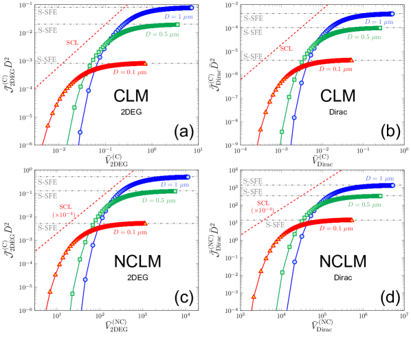
In Figs. 7, the - curves of CLM [Figs. 7(a) and (b)] and NCLM [Figs. 7(c) and (d)] models are plotted by simultaneously solving Eqs. (33), (34) and (36). Three vacuum gap distances are used: 0.1 m, 0.5 m and 1 m. The Fermi level is set to eV. At small , the increases approximately exponentially with as a result of the field-induced quantum tunneling. The - curves shift towards the SCL limit (dashed curve in Fig. 7) as increases due to the building up of space charge in the vacuum gap. However, when is further increased, the curves reach a plateau without dwelling into the full SCL regime. This peculiar absence of full SCL flow can be explained by the saturated emission, which is a source-limited mechanism. At sufficiently high voltage, the emission current densities saturated. In this case, the 2D-material-based cathode fails to supply the required magnitude of charge current to establish a full SCL flow. This leads to a remarkable consequence: SCL emission is completely absent in 2D-material-based vacuum diode at nanometer and micrometer scales, with practical bias voltage range of kV.
| Normalization constant | (m) | (m) | (V) | (m) | ||
|---|---|---|---|---|---|---|
| Numerical value | 8.28 |
| Normalization constant | (m) | (m) | (V) | (m) | ||
|---|---|---|---|---|---|---|
| Numerical value | 535 | 0.30 |
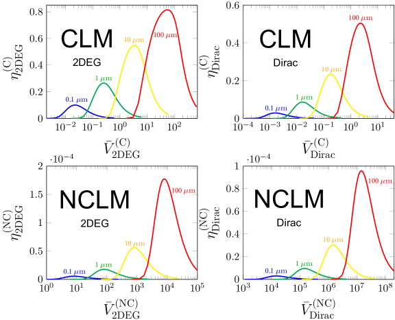
The strength of SCL effect can be quantified by the ratio, , where signifies the onset of full SCL flow. In Fig. 8, the ’s of CLM and NCLM models are plotted for ten values of ranging from m to 100 m. The curves briefly peak and decline due to the onset of saturated emission. For CLM models, the maximum with m are found to be and [Figs. 8(a) and (b)], thus suggesting only a maximal of % and % of the SCL limit is achievable in 2D material with parabolic and linear lateral energy dispersion, respectively. This suppression is even more dramatic for NCLM models [Figs. 8(c) and (d)] in which the maximum are in the order of for both types of lateral energy dispersions. This negligibly small magnitude of suggests that SCL flow is practically absent if the SFE process does not conserve lateral momentum. Even for a vacuum gap size of 100 m which requires an exceedingly large bias voltage of V, the CLM model can maximally achieve and . The onset of full SCL emission remains out of reach. In calculating , we have estimated . By tuning to the NCLM process to the unrealistic full-strength value of , we have and , which are still fractions of the full SCL limit.
We now estimate the value of bias voltage at which the saturated emission current density can be observed experimentally. The onset of the saturated emission can be estimated from Fig. 8 as the bias voltage at which the curve peaks. For CLM models with m, the onset of saturated emission occurs at and [Figs. 8(a) and (b)]. Consider a conservative value of field enhancement factor of , we obtain V and V in SI unit. For NCLM models, the onset of saturated emission occurs at and [Figs. 8(c) and (d)], which correspond to V and V. These values are well within the achievable voltage range in experiments. Thus, the saturated emission and the absence of SCL flow shall be observable in monolayer and bilayer graphene surface field emitters.
V Discussion
V.1 Physical interpretation of the ‘time’-like parameter in Sinha-Lee’s ‘time’-constant-based thermionic emission model
We now discuss the relation between the generalized formalism for 2D material electron emission developed above and Sinha-Lee’s ‘time’-constant-based TE model for graphene sinha . We shall show that our model can recover the physical meaning of the arbitrarily-defined ‘time’-parameter, namely , in Sinha-Lee’s model.
In Sinha-Lee’s model, the -integral in the emission current density equation is replaced by the ‘time’-like parameter, , i.e.
In obtaining Eq. (V.1), the over-barrier transmission probability is assumed to take the form of . This -dependent transmission probability, rather than -dependent one, immediately suggests that the Sinha-Lee TE model belongs to the class of NCLM model. The physical interpretation of remains fuzzy in this model. As carries the physical dimension of time, it is hypothesized that it represents the time scale of how fast electrons are extracted from graphene surface.
Here, based on the NCLM model developed in Eq. (12b), a concrete physical meaning of can be recovered. By using the standard TE approximations of and , the NCLM model of graphene TE can be solved as
| (43) | |||||
By equating Eqs. (V.1) and (43), we can write the ‘time’-like parameter in terms of physical terms, i.e.
| (44) |
Here, the physics of becomes apparent: is directly related to the strength of NCLM process, the 2D material thickness and the out-of-plane bound state electron velocity. This suggests that interpreting as the time scale of how fast electrons are extracted from the thermionic emitter is not appropriate since is the 2D material thickness rather than the separation between the electron emitter and the collector. Using nm, eV, m/s and setting the NCLM process to the full strength of , the lower limit of can be predicted as fs.
The value of varies depending on the quality of the interface. For graphene/silicon and graphene/Pd contacts, the experimentally extracted ’s are ps and ps, respectively sinha . These values correspond to and , respectively. In the above sections, we choose in the calculation of NCLM emission models. Note that even in the case of unrealistic , the unconventional saturated emission and the absence of full SCL flow reported in this work remain robust. Such effects becomes even more profound for smaller value of .
V.2 Summary and outlooks
For the ease-of-use of the models developed above in the analysis of experimental data, we summarize in Table III the field-induced surface electron emission models in empirical forms where only the -dependences are explicitly shown. We note that the model can be further improved, for example, by using the exact expression of the triangular barrier tunneling probability, including the image potential and generalization of the model to include thermionic contributions forbes2 ; forbes3 ; jensen ; jensen2 . Nonetheless, we expect these refinements to only quantitatively alter the results. The dimensionality-induced saturated emission and the strong suppression of SCL electron flow shall qualitatively remains the same. Finally, we remark that although the two versions of vertical emission models developed above, i.e. with and without lateral momentum conservation, exhibit different forms in general, they both converge to the same unconventional scaling relation of at high field. This suggests that the modified FN-plot in Eq. (15) shall be universally applicable to the cases of both conversing and non-conserving lateral momentum. Further experimental and ab initio computational works are required to pin down the mechanism (i.e. CLM or NCLM) underlying the field-induced vertical electron emission from the surface of 2D materials.
| Model | Lateral energy dispersion () | Empirical form | Full expression |
|---|---|---|---|
| FN Law | Parabolic | Eq. (1b) | |
| CLM | parabolic | Eq. (14a) | |
| linear | Eq. (14b) | ||
| NCLM | Parabolic | Eq. (17a) | |
| Linear | Eq. (17b) | ||
| (Low-field regime) | Parabolic | Eq. (18a) | |
| Linear | Eq. (18b) | ||
| (High-field regime) | Parabolic | Eq. (20a) | |
| Linear | Eq. (20b) |
VI Conclusion
In conclusion, we have developed analytical and semi-analytical models of field-induced vertical electron emission from the surface of 2D materials by explicitly taking into account the reduced dimensionality, non-parabolic energy dispersion, non-conservation of the lateral momentum, finite-temperature and space-charge-limited effects. Our proposed models are more consistent with the physical properties of 2D-material-based field emitter, which are emerging rapidly in the past decade. We show that the conventional Fowler-Nordheim paradigm for 3D-bulk-material-based field emitter is no longer valid for 2D materials and it should be replaced by the modified models developed above. The reduced-dimensionality of 2D material leads to the occurrence of saturated emission and the strong suppression of space-charge-limited electron flow in nanometer-and micrometer-scale vacuum devices. The generalized 2D material field emission models can be readily applied to describe the charge transport physics in 2D-material-based electrical contact, which is crucially important in the design and engineering of 2D-material-based nanoelectronic and optoelectronic devices, and will be discussed in a separate work.
acknowledgment
We thank Ji Xu and Qilong Wang for helpful discussions and for providing the experimental data of graphene surface field emission. We thank Shi-Jun Liang for stimulating discussions. This work is supported by A*STAR-IRG (A1783c0011) and AFOSR AOARD (FA2386-17-1-4020).
References
- (1) A. Sommerfeld, ‘Zur elektronentheorie der metalle’, Naturwissenschaften 15, 852 (1927).
- (2) For a historical review, see L. Hoddeson, and G. Baym, ‘The development of the quantum-mechanical electron theory of metals: 1928 – 1933’, Rev. Mod. Phys. 59, 287 (1987).
- (3) O. W. Richardson, ‘Some applications of the electron theory of matter’, Phil. Mag. 23, 594 (1912); S. Dushman, ‘Electron emission from metals as a function of temperature’, Phys. Rev. 21, 623 (1923); O. W. Richardson, The distribution of the molecules of gas in a field of force, with applications to the theory of electrons, Phil. Mag. 28, 633 (1914); O. W. Richardson, The influence of gases on the emission of electrons and ions from hot metals, Proc. Roy. Soc. A 91, 524 (1915).
- (4) R. H. Fowler, and L. Nordheim, ‘Electron emission in intense electric fields’, Proc. R. Sot. London Ser. A 119, 173 (1928).
- (5) The emission constants are given as , and where and are the Planck constant and reduced Planck constant, respectively.
- (6) P. Zhang, A. Valfells, L. K. Ang, J. W. Luginsland, and Y. Y. Lau, ‘100 years of the physics of diodes’, Appl. Phys. Rev. 4, 011304 (2017).
- (7) W. W. Dolan, and W. P. Dyke, ‘Temperature-and-field emission of electrons from metals’, Phys. Rev. 95, 327 (1954).
- (8) E. L. Murphy, and R. H. Good, Jr., ‘Thermionic emission, field emission, and the transition region’ Phys. Rev. 102, 1464 (1956).
- (9) R. E. Burgess, H. Kroemer, and J. M. Houston, ‘Corrected values of Fowler-Nordheim field emission functions and , Phys. Rev. 90, 515 (1953).
- (10) R. Stratton, ‘Theory of field emission from semiconductors’, Phys. Rev. 125, 67 (1962).
- (11) R. G. Forbes, ‘Field emission: New theory for the derivation of emission area from a Fowler-Nordheim plot’, J. Vac. Sci. Tech. B 17, 526 (1999).
- (12) R. G. Forbes, ‘Low-macroscopic-field electron emission from carbon films and other electrically nanostructured heterogeneous materials: hypotheses about emission mechanism’, Solid State Electron. 45, 779 (2001).
- (13) R. G. Forbes, and J. H. B. Deane, ‘Reformulation of the standard theory of Fowler-Nordheim tunnelling and cold field electron emission’, Proc. Roy. Soc. A 463, 2907 (2007).
- (14) R. G. Forbes and J. H. B. Deane, ‘Transmission coefficients for the exact triangular barrier: An exact general analytical theory that can replace Fowler & Nordheim’s 1928 theory’, Proc. R. Soc. A 467, 2927 (2011).
- (15) K. L. Jensen, P. G. O’Shea, and D. W. Feldman, ‘Generalized electron emission model for field, thermal, and photoemission’, Appl. Phys. Lett. 81, 3867 (2002).
- (16) K. L. Jensen, ‘General formulation of thermal, field, and photoinduced electron emission’, J. Appl. Phys. 102, 024911 (2007).
- (17) K. L. Jensen, D. A. Shiffler, J. J. Petillo, Z. Pan, and J. W. Luginsland, ‘Emittance, surface structure, and electron emission’, Phys. Rev. ST Accel. Beams 17, 043402 (2014).
- (18) A. Kyritsakis and J. P. Xanthakis, ‘Derivation of a generalized Fowler-Nordheim equation for nanoscopic fieldemitters’, Proc. R. Soc. A 471, 20140811 (2015).
- (19) S.-D. Liang, and L. Chen, ‘Generalized Fowler-Nordheim theory of field emission of carbon nanotubes’, Phys. Rev. Lett. 101, 027602 (2008).
- (20) X. Wei, Y. Bando, and D. Golberg, ‘Electron emission from individual graphene nanoribbons driven by internal electric field’, ACS Nano 6, 705 (2012).
- (21) X. Wei, D. Golberg, Q. Chen, Y. Bando, and L. Peng, ‘Phonon-assisted electron emission from individual carbon nanotubes’, Nano Lett. 11, 734 (2010).
- (22) C. J. Edgcombe, ‘Development of Fowler-Nordheim theory for a spherical field emitter’, Phys. Rev. B 72, 045420 (2005).
- (23) . T. Holgate and M. Coppins, ‘Field-induced and thermal electron currents from earthed spherical emitters’, Phys. Rev. Applied 7, 044019 (2017).
- (24) S.-J. Liang, and L. K. Ang, ‘Electron thermionic emission from graphene and a thermionic energy converter’, Phys. Rev. Appl. 3, 014002 (2015).
- (25) Y. S. Ang, and L. K. Ang, ‘Current-temperature scaling for a Schottky interface with nonparabolic energy dispersion’, Phys. Rev. Appl. 6, 0340133 (2016).
- (26) Sinha, and J.-U. Lee, ‘Ideal graphene/silicon Schottky junction Diodes’, Nano Lett. 14, 4660 (2014).
- (27) S.-J. Liang, W. Hu, A. Di Bartolomio, S. Adam, L. K. Ang, ‘A modified Schottky model for graphene-semiconductor (3D/2D) contact: A combined theoretical and experimental study’, 2016 IEEE International Electron Devices Meeting (IEDM), 14.4.1, doi: 10.1109/IEDM.2016.7838416 (2016).
- (28) S. Misra, M. Upadhyay Kahaly, and S. K. Mishra, ‘Thermionic emission from monolayer graphene, sheath formation and its feasibility towards thermionic converters’, J. Appl. Phys. 121, 065102 (2017).
- (29) S. Misra, M. Upadhyay Kahaly, and S. K. Mishra, ‘Efficient utilization of multilayer graphene towards thermionic convertors’, Int. J. Ther. Sci. 121, 358 (2017).
- (30) S.-J. Liang, B. Liu, K. Zhou, and L. K. Ang, ‘Thermionic energy conversion based on graphene van der Waals heterostructure’, Sci. Rep. 7, 46211 (2017).
- (31) M. Massicotte et al, ‘Photo-thermionic effect in vertical graphene heterostructures’, Nature Commun. 7, 12174 (2016).
- (32) For a review of graphene field emission, see Y. S. Ang, S.-J. Liang, and L. K. Ang, ‘Theoretical modeling of electron emission from graphene’, MRS Bulletin 42, 505 (2017).
- (33) H. M. Wang, Z. Zheng, Y. Y. Wang, J. J. Qiu, Z. B. Guo, Z. X. Shen, and T. Yu, ‘Fabrication of graphene nanogap with crystallographically matching edges and its electron emission properties’, Appl. Phys. Lett. 96, 023106 (2010).
- (34) S. Kumar, G. S. Duesberg, R. Pratap, and S. Raghavan,‘Graphene field emission devices’, Appl. Phys. Lett. 105, 103107 (2014).
- (35) D. Ye, S. Moussa, J. D. Ferguson, A. A. Baski, and M. S. El-Shall, ‘Highly efficient electron field emission from graphene oxide sheets supported by nickel nanotip arrays’, Nano Lett. 12, 1265 (2012).
- (36) J. Xu et al, ‘Field emission of wet transferred suspended graphene fabricated on interdigitated electrodes’, ACS Appl. Mater. Interfaces 8, 3295 (2016).
- (37) G. Wu, X. Wei, Z. Zhang, Q. Chen, and L. Peng, ‘A graphene-based vacuum transistor with a high ON/OFF current ratio’, Adv. Func. Mater. 25, 5972 (2015).
- (38) L. Sun, X. Zhou, Z. Lin, T. Guo, Y. Zhang, and Y. Zeng, ‘Effects of ZnO quantum dots decoration on the field emission behavior of graphene’, ACS Appl. Mater. Interfaces 8, 31856 (2016).
- (39) S. Sun, L. K. Ang, D. Shiffler, and J. W. Luginsland, ‘Klein tunnelling model of low energy electron field emission from single-layer graphene sheet’, Appl. Phys. Lett. 99, 013112 (2011).
- (40) S.-J. Liang, S. Sun, and L. K. Ang, ‘Over-barrier side band electron emission from graphene with time-oscillating potential’, Carbon 61, 294 (2013).
- (41) R. Z. Wang, H. Yan, B. Wang, X. W. Zhang, and X. Y. Hou, ‘Field emission enhancement by the quantum structure in an ultrathin multilayer planar cold cathode’, Appl. Phys. Lett. 92, 142102 (2008).
- (42) X. Wei, Q. Chen, and L. Peng, ‘Electron emission from two-dimensional crystal with atomic thickness’, AIP Adv. 3, 042130 (2013).
- (43) A. Malesevic, R. Kemps, A. Vanhulsel, M. P. Chowdhury, A. Volodin, and C. van Haesendonck, ‘Field emission from carbon nanotubes and its application to electron sources’, J. Appl. Phys. 104, 084301 (2008).
- (44) G. Eda, H. E. Unalan, N. Rupesinghe, G. A. J. Amaratunga, and M. Chhowalla, ‘’Field emission from graphene based composite thin films, Appl. Phys. Lett. 93, 233502 (2008).
- (45) M. Qian, T. Feng, H. Ding, L. Lin, H. Li, Y. Chen, and Z. Sun, ‘Electron field emission from screen-printed graphene films’, Nanotechnology 20, 425702 (2009).
- (46) Z.-S. Wu, S. Pei, W. Ren, D. Tang, L. Gao, B. Liu, F. Li, C. Liu, and H.-M. Cheng, ‘Field emission of single-layer graphene films prepared by electrophoretic deposition‘, Adv. Mater. 21, 1756 (2009).
- (47) C.-K. Huang, Y. Ou, Y. Bie, Q. Zhao, and D. Yu, ‘Well-aligned graphene arrays for field emission displays’, Appl. Phys. Lett. 98, 263104 (2011).
- (48) H. Yamaguchi et al., ‘Field emission from atomically thin edges of reduced graphene oxide’, ACS Nano 5, 4945 (2011).
- (49) S. Santandrea, F. Giubileo, V. Grossi, S. Santucci, M. Passacantando, T. Schroeder, G. Lupina, and A. Di Bartolomeo, ‘Field emission from single and few-layer graphene flakes’, Appl. Phys. Lett. 98, 163109 (2011).
- (50) U. A. Palnitka, R. V. Kashid, M. A. More, D. S. Joag, L. S. Panchakarla, and C. N. R. Rao, ‘Remarkably low turn-on field emission in undoped, nitrogen-doped, and boron-doped graphene’, Appl. Phys. Lett. 97, 063102 (2010).
- (51) N. Soin et al., ‘Enhanced and stable field emission from in situ nitrogen-doped few-layered graphene nanoflakes’, J. Phys. Chem. C 115, 5366 (2011).
- (52) V. I. Kleshch, D. A. Bandurin, A. S. Orekhov, S. T. Purcell, and A. N. Obraztsov, ‘Edge field emission of large-area single layer graphene’, Appl. Surf. Sci. 357, 1967 (2015).
- (53) G. Wu, X. Wei, S. Gao, Q. Chen, and L. Peng, ‘Tunable graphene micro-emitters with fast temporal response and controllable electron emission’, Nature Commun. 7, 11513 (2016).
- (54) M. Z. Yusop, G. Kalita, Y. Yaakob, C. Takahashi, and M. Tanemura, ‘Field emission properties of chemical vapor deposited individual graphene’, Appl. Phys. Lett. 104, 093501 (2014).
- (55) A. Di Bartolomeo, F. Giubileo, L. Iemmo, F. Romeo, S. Russo, S. Unal, M. Passacantando, V. Grossi, and A. M. Cucolo, ‘Leakage and field emission in side-gate graphene field effect transistors’, Appl. Phys. Lett. 109, 023510 (2016).
- (56) L. Iemmo et al, ‘Graphene enhanced field emission from InP nanocrystals’, arXiv:1708.01877 (2017).
- (57) X.-Z. Qin, W.-L. Wang, N.-S. Xu, Z.-B. Li, and R. G. Forbes, ‘Analytical treatment of cold field electron emission from a nanowall emitter, including quantum confinement effects’, Proc. R. Soc. A 467, 1029 (2011).
- (58) Z. Xiao, J. She, S. Deng, Z. Tang, Z. Li, J. Lu, and N. Xu, ‘Field electron emission characteristics and physical mechanism of individual single-layer graphene’, ACS Nano 4, 6332 (2010).
- (59) W. Wang, X. Qin, N. Xu, and Z. Li, ‘Field electron emission characteristic of graphene’, J. Appl. Phys. 109, 044304 (2011).
- (60) J. P. Barbour, W. W. Dolan, J. K. Trolan, E. E. Martin, and W. P. Dyke, ‘Space-charge effects in field emission’, Phys. Rev. 92, 45 (1953).
- (61) Y. Y. Lau, Y. Liu, and R. K. Parker, ‘Electron emission: From the Fowler–Nordheim relation to the Child–Langmuir law’, Phys. Plasma 1, 2082 (1994).
- (62) K. L. Jensen, ‘Space charge effects in field emission: Three dimensional theory’, J. Appl. Phys. 107, 014905 (2010).
- (63) R. G. Forbes, ‘Exact analysis of surface field reduction due to field-emitted vacuum space charge, in parallel-plane geometry, using simple dimensionless equations’, J. Appl. Phys. 104, 084303 (2008).
- (64) P. Zhang, ‘Scaling for quantum tunneling current in nano- and subnano-scale plasmonic junctions’, Sci. Rep. 5, 9826 (2015).
- (65) C. D. Child, Phys. Rev. 32, 492 (1911); I. Langmuir, ibid 21, 419 (1921).
- (66) Y. S. Ang, M. Zubair and L. K. Ang, ‘Relativistic space-charge-limited current for massive Dirac fermions’, Phys. Rev. B 95, 165409 (2017).
- (67) A. Allain, J. Kang, K. Banergee, and A. Kis, ‘Electrical contacts of two-dimensional semiconductors’, Nature Mater. 14, 1195 (2015).
- (68) Y. Xu et al, ‘Contacts between two- and three-dimensional materials: Ohmic, Schottky, and - heterojunctions’, ACS Nano 10, 4895 (2016).
- (69) A. Di Bartolomeo, ‘Graphene Schottky diodes: An experimental review of the rectifying graphene/semiconductor heterojunction’, Phys. Rep. 606, 1 (2016).
- (70) D. Jariwala, T. J. Marks, and M. C. Hersam, ‘Mixed-dimensional van der Waals heterostructures’, Nature Mater. 16, 170 (2017).
- (71) L. D. N. Mouafo et al, ‘Tuning contact transport mechanisms in bilayer MoSe2 transistors up to Fowler-Nordheim regime’, 2D Mater. 4, 015037 (2017).
- (72) R. Grassi, Y. Wu, S. J. Koester, and T. Low, ‘Semianalytical model of the contact resistance in two-dimensional semiconductors’, Phys. Rev. B 96, 165439 (2017).
- (73) S. de Vega, and F. J. G. de Abajo, ‘Plasmon generation through electron tunneling in graphene’, ACS Photon. 4, 2367 (2017).
- (74) S. V. Meshkov, ‘Tunneling of electrons from a two-dimensional channel into the bulk’, Sov. Phys. JETP 64, 1337 (1986).
- (75) D. Vashaee, and A. Shakouri, ‘Improved thermoelectric power factor in metal-based superlattices’, Phys. Rev. Lett. 92, 106103 (2004).
- (76) D. Vashaee, and A. Shakouri, ‘Electronic and thermoelectric transport in semiconductor and metallic superlattices’, J. Appl. Phys. 95, 1233 (2004).
- (77) M. F. O’Dwyer, R. A. Lewis, C. Zhang, and T. E. Humphrey, ‘Electronic efficiency in nanostructured thermionic and thermoelectric devices’, Phys. Rev. B 72, 205330 (2005).
- (78) R. Kim, C. Jeong, and M. Lundstrom, ‘On momentum conservation and thermionic emission cooling’, J. Appl. Phys. 107, 054502 (2010).
- (79) H. Zhu, J. Wang, Z. Gong, Y. D. Kim, J. Hone, and X.-Y. Zhu, ‘Interfacial charge transfer circumventing momentum mismatch at two-dimensional van der Waals heterojunctions’, Nano Lett. 17, 3591 (2017).
- (80) J.H. Chen, C. Jang, M. S. Fuhrer, E. D. Williams1, and M. Ishigami, ‘Charged impurity scattering in graphene’, Nature Phys. 4, 377 (2008).
- (81) T. Ando, ‘Screening effect and impurity scattering in monolayer graphene’, J. Phys. Soc. Jpn. 75, 074716 (2006).
- (82) E. H. Hwang and S. Das Sarma, ‘Dielectric function, screening, and plasmons in two-dimensional graphene’, Phys. Rev. B 75, 205418 (2007).
- (83) L. A. Ponomarenko et al, ‘Effect of a high- environment on charge carrier mobility in graphene’, Phys. Rev. Lett. 102, 206603 (2009).
- (84) C.-F. Chen et al, ‘Controlling inelastic light scattering quantum pathways in graphene’, Nature 471, 617 (2011).
- (85) Y.-J. Yu, Y. Zhao, S. Ryu, L. E. Brus, K. S. Kim, and P. Kim, ‘Tuning the graphene work function by electric field effect’, Nano Lett. 9, 3430 (2009).
- (86) K. Xu et al., ‘Direct measurement of Dirac point energy at the graphene/oxide interface’, Nano Lett. 13, 131 (2013).
- (87) C. Christodoulou et al., ‘Tuning the work function of graphene-on-quartz with a high weight molecular acceptor’, J. Phys. Chem. C 118, 4784 (2014).
- (88) For details of finite square potential well model and simulation of graphene, see Supporting Information of Ref. vega . Note that we use eV reported in xu_wf ; chris , rather than the 4.7 eV used in Ref. vega .
- (89) A. H. Castro Neto, F. Guinea, N. M. R. Peres, K. S. Novoselov, and A. K. Geim, ‘The electronic properties of graphene’, Rev. Mod. Phys. 81, 109 (2009).
- (90) E. McCann, D. S. L. Abergel, and V. I. Fal’ko, ‘Electrons in bilayer graphene’, Solid State Commun. 143, 110 (2007).
- (91) J. Li et al, ‘Effective mass in bilayer graphene at low carrier densities: The role of potential disorder and electron-electron interaction’, Phys. Rev. B 94, 161406(R) (2016).
- (92) S. R. Suryawanshi, and M. A. More, ‘Exfoliated 2D black phosphorus nanosheets: Field emission studies’, J. Vac. Sci. Tech. B 34, 041803 (2016).
- (93) Y. Jiang, R. Roldan, F. Guinea, and T. Low, ‘Magnetoelectronic properties of multilayer black phosphorus’, Phys. Rev. B 92, 085408 (2015).
- (94) F. W. Han, W. Xu, L. L. Li, C. Zhang, H. M. Dong, and F. M. Peeters, ‘Electronic and transport properties of -type monolayer black phosphorus at low temperatures’, Phys. Rev. B 95, 115436 (2017).
- (95) E. Gruber et al, ‘Ultrafast electronic response of graphene to a strong and localized electric field’, Nature Commun. 7, 13948 (2016).
- (96) M. Abramowitz, and I. A. Stegun, ‘Handbook of mathematical functions: with formulas, graphs, and mathematical tables’, Dover Publications (USA, 1965).
-
(97)
The Sommerfeld expansion is given as
where is a given function of and is the chemical potential which can be approximated, up to second order in , from the Sommerfeld expansion by setting . For parabolic and linear energy dispersion, is obtained as and , respectively. - (98) Y. Y. Lau, D. Chernin, D. G. Colombant, and P.-T. Ho, ‘Quantum extension of Child-Langmuir law’, Phys. Rev. Lett. 66, 1446 (1991).
- (99) L. K. Ang, T. J. T. Kwan, and Y. Y. Lau, ‘New scaling of Child-Langmuir law in the quantum regime’, Phys. Rev. Lett. 91, 208303 (2003).
- (100) W. S. Koh and L. K. Ang, ‘Transition of field emission to space-charge-limited emission in a nanogap’, Appl. Phys. Lett. 89, 183107 (2006).