Also at ]Faculty of Mathematics and Physics, Charles University, Ke Karlovu 5, CZ-121 16 Praha 2, Czech Republic
Quantum Dragon Solutions for Electron Transport through Nanostructures based on Rectangular Graphs
G. Inkoom
M.A. Novotny
[
man40@msstate.eduDepartment of Physics and Astronomy
Mississippi State University
Mississippi State, MS 39762-5167
USA
Abstract
Electron transport through nanodevices of atoms in a single-layer rectangular arrangement
with free (open) boundary conditions parallel to the direction of the current flow is studied
within the single-band tight binding model.
The Landauer formula gives the electrical conductance to be a function of the electron
transmission probability, , as a function of the energy of the incoming electron.
A quantum dragon nanodevice is one which has a perfectly conducting channel,
namely for all energies which are transmitted
by the external leads even though there may be arbitrarily strong electron scattering.
The rectangular single-layer systems are shown to be able to be quantum dragon devices,
both for uniform leads and for dimerized leads.
The quantum dragon condition requires appropriate lead-device connections and
correlated randomness in the device.
Electron Transport, Quantum Dragons, Nanodevices
pacs:
73.63.-b, 78.67.Bf, 85.35.-p
††preprint: MAN_MSU_CUP-2017-1
I Introduction
The confluence of the approaching end of Moore’s law for electronics WALD2016
and the increasing ability of experimentally being able to manipulate, fabricate, and measure
at the nanoscale level TAKA2010
is the reason rapid progress in nanoelectronics is being made PUER2017 .
Of particular interest is the electron transmission properties of
nanodevices DATTA1995 ; FerryGoodnick1997 ; TODO2002 ; DATTA2005 ,
including electron transmission in molecular electronics ZIMB2011 ; CUEV2017 .
Due to the quantum mechanics underlying nanodevices, properties of coherent
electron transport can be very different from those expected at the macroscopic scale.
As shown by Landauer LAND57 , of central importance to nanodevices is the
electron transmission, , of the nanodevice when it is connected to leads attached
to a source and a sink of electrons. As in macroscopic systems, one desires the
electrical conductance (the inverse of the electrical resistance) in an Ohm’s law
relationship where is the electrical current flowing through the device and
is the applied electrical voltage difference. At low temperatures the Landauer
formula gives the electrical conductance FerryGoodnick1997 ; BAGW1989
(1)
for two probe or four probe measurements. Here is the
quantum of conductance, with the charge of the electron, Planck’s constant,
and the factor of two is due to the spin of the electron.
The transmission is a function of the energy of an incoming electron,
and in Eq. (1) the transmission at the Fermi energy enters.
The power of the shot noise of the nanodevice is LESO1989 ; BUTT1990 ; KUMA1996 ; OUIS2013
(2)
which is zero if .
In this investigation we are interested in a perfectly conducting channel, namely
where for all energies which can propagate through long
leads. There are different possibilities for the existence of perfectly conducting channels
in coherent electron propagation. These possibilities include:
•
Ballistic propagation.
If there is no scattering in the device,
electrons propagate ballistically, and . For ballistic propagation,
the two different behaviors for in Eq. (1) have been observed
experimentally in the same sample of a very pure semiconductor DEPI2001 .
•
Long-range randomness.
For example, in zigzag carbon nanoribbons when there is random long-range scattering,
the average in two probe measurements as the
length of the device increases WAKA2007 .
•
Surface states in topological insulators.
In topological insulators, surface states can lead to perfectly
conducting channels which are protected against scattering due to
disorder MATS2015 .
•
Quantum dragons.
In 2014, one of the authors discovered a
large class of nanodevices MANdragon2014
which can have arbitrarily strong scattering,
but because the scattering is correlated they can have for any .
These nanodevices, with strong scattering but with
a perfectly conducting channel, were named ‘quantum dragons’ in ref. MANdragon2014, .
Sometimes nanodevices with a perfectly conducting channel have been said to
be metallic or ballistic, due to the electrical conductance given by Eq. (1). Examples
are armchair single walled carbon nanotubes OUYA2001 ; KONG2001 and graphene nanoribbons
BARI2014 ; CELI2016 . TEM and SEM investigations of gold point contacts
have also been performed Erts2000 .
Single layer thick carbon nanotubes and graphene nanoribbons have been fabricated,
and their intriguing properties studied BARI2014 ; CELI2016 . These systems are all based
on an underlying hexagonal lattice. Single-walled carbon nanotubes in the armchair arrangement
have been experimentally shown to have metallic behavior OUYA2001 ,
often in the literature said to exhibit ballistic electron propagation WHIT1998 .
However, one needs to be careful to
remember only if an armchair single-walled carbon nanotube is connected
to appropriate leads in the correct fashion OUYA2001 ; MANdragon2014 .
The name quantum dragons denotes such devices may be formed by joining different
types of nanodevices, their length is typically longer than any other dimension, and
they are invisible to electrons which propagate in the leads.
The quantum dragon nanodevices published in ref. MANdragon2014, all had cylindrical symmetry.
In this paper we investigate quantum dragon nanodevices without cylindrical symmetry.
In particular, we investigate quantum dragons in single-layer thick nanodevices based
on an underlying rectangular graph, with open (free) boundary conditions perpendicular
to the direction of the current flow.
Recently, some single layer thick materials based on rectangular lattices have been
synthesized.
One example is free-standing single-atom-thick iron membranes ZHAO2014 ,
and another is copper oxide monolayers YIN2016 ; KANO2017 .
Other examples are 2D materials and van der Waal heterostructures have recently
been reviewed NOVO2016 .
These experimental systems, and the possibility of many more 2D systems based on
rectangular lattices, provide the impetus to study whether nanodevices based on
underlying rectangular graphs can have , and in particular whether
such systems can be quantum dragons.
The paper is organized as follows.
In Sec. II, the method of calculating for non-dimerized
devices and leads is presented. The method used is the matrix method DCA2000 .
Sec. III gives the method to obtain quantum dragon solutions via
the exact mapping and tuning process for systems based on rectangular graphs.
Sec. IV contains example numerical calculations of non-dimerized quantum dragons,
thereby better illustrating the concept.
Sec. V has our conclusions and further discussion.
The main text is supplemented with a number of appendices.
A detailed discussion of the example devices shown is presented in App. A for devices without disorder and in App. B for devices with disorder.
The matrix method to calculate for dimerized leads
is derived in App. C. Quantum dragon solutions for nanodevices based on rectangular graphs with dimerized leads is
presented in App. D. The relationship between the matrix method used in this article and the commonly
used Green’s function method to calculate is given in App. E. Appendix F shows in mathematical detail how quantum dragon solutions arise in the case of
two slices in the nanodevice.
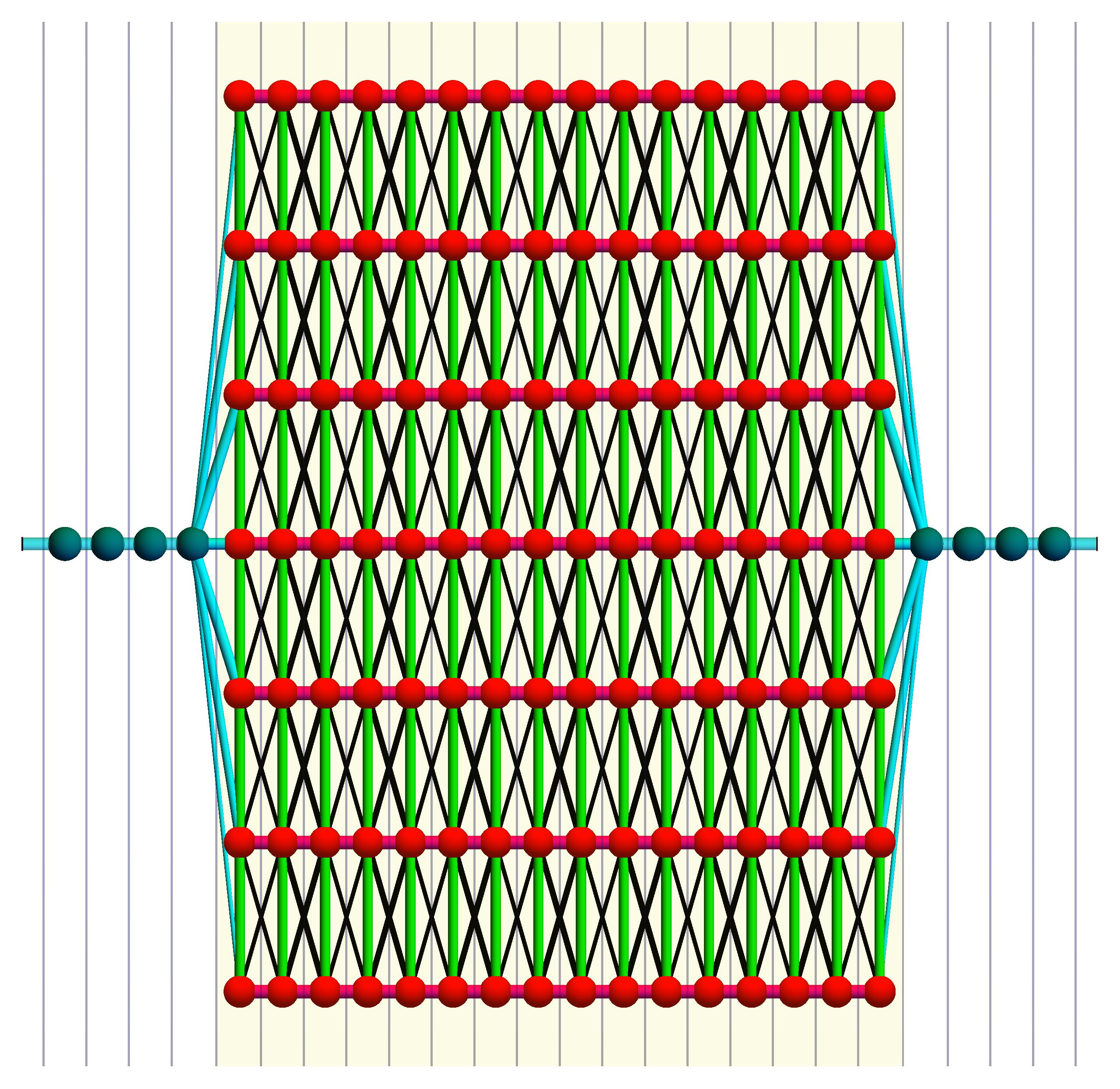
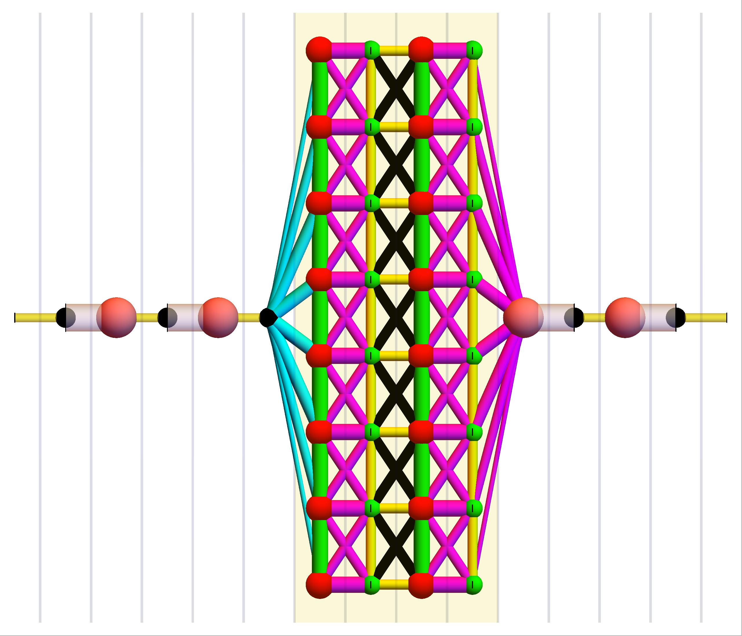
Figure 1:
(Color online.)
An example of leads connected to a planar rectangular nanodevice
with and .
Leads and device are both uniform and without disorder.
See Appendix A.1 for a complete description.
II Transmission Calculations
The electron transmission is found from the solution of the time-independent
Schrödinger equation for the nanodevice and leads. Although solutions
using density functional theory,
as in the review ZIMB2011 , are possible, this imposes a limit on the number of
atoms which can be studied in the nanodevice and furthermore limits one to
numerical investigations. Therefore, here we study the nanodevice and leads within
the single-band tight binding (TB) model. In the TB model the important quantities are
the on site energy (at the location of every atom), , and the hopping
between atoms, denoted in this article by either or .
The hopping terms come from overlaps of electron
wavefunctions between atoms located near one another, so in the device and the leads
we limit ourselves to nearest-neighbor (nn) and next-nearest-neighbor (nnn) hopping terms.
In most cases the hopping terms are negative, so we put in the negative sign ‘by hand’
and let or stand for the magnitude of the hopping.
Four advantages of the TB model for electron transport calculations are detailed
in ref. TODO2002, .
We only analyze the two terminal measurement setup.
Within the TB model, the matrix equation to solve is
(3)
where is the infinite identity matrix,
is the infinite matrix for the two semi-infinite leads and the device,
and is the energy of the incoming electrons.
In the text in the main article, we concentrate on uniform (not dimerized)
leads attached to a rectangular device, as in Fig. 1.
The case where the leads are dimerized has the matrix method solution
derived in App. C and analyzed in App. D. We have freedom in choosing our
zero of energy, so we choose the on site energy of the lead atoms to be zero.
The hopping strength between lead atoms we take to be . In many cases
theorists take to be the unit of energy and set it to
unity MANdragon2014 ; DCA2000 ; BOET2011 ; NOVO2014 , but we
will keep throughout in order to make better connection with the
dimerized leads in the appendices. We assume our nanodevice has an underlying
rectangular graph, as in Fig. 1.
Every slice (every column) of the nanodevice has atoms, and there are
slices. Within column , every atom has the same on site energy
and the same nn hopping .
Between columns and there can be nn hopping of strength
and nnn hopping of strength .
The device can be considered to be a planar rectangular
array of atoms when there is no disorder, as in Fig. 1,
when all TB parameters are the same,
that is , , , and .
When there is disorder in the TB parameters , ,
and , the underlying graph is still rectangular but the
nanodevice need not remain planar, as in Fig. 2.
Figure 2:
(Color online.)
An example of uniform leads connected to a disordered, rectangular device
with and .
The same device is shown in the top (top view) and
bottom (oblique view) of the figure.
See Appendix B for a complete description.
We use the matrix method DCA2000 to calculate the transmission, , because
the mapping and tuning method to find quantum dragons takes advantage of
the matrix structure. App. E gives the relationship between the commonly used
Green’s function method
DATTA1995 ; FerryGoodnick1997 ; TODO2002 ; DATTA2005 ; ZIMB2011 ; CUEV2017 ; TRIO2016
and the matrix method.
For dimerized leads the method is derived in App. C, while for uniform leads the matrix method was put forward in 2000 DCA2000 .
Unless otherwise explicitly stated or indicated by subscripts, the dimension of
all vectors is and all matrices are of size . The transmission
is calculated by where is calculated by the
inverse of a matrix which has the form
(written for )
(4)
where the vector () contains the TB hopping terms
between the incoming left (outgoing right) lead and the atoms in the
first (last) slice of the device.
The intra-slice TB terms, here and , are in the
matrices with the
identity matrix.
Note the energy is only present in the diagonal elements of .
The TB intra-slice matrix is
(5)
and the inter-slice TB terms are
(6)
The matrix is defined by
(7)
and has this form because we study a rectangular lattice,
allow only nn hopping within each slice, and allow only nn and nnn
hopping between slices.
The matrix contains the part of the Hamiltonian which
includes all TB parameters within slice , while
is the part of the Hamiltonian containing the TB parameters which are
the hopping terms between atoms in slices numbered and .
The wavevector of the electron in the leads is given by
(8)
where the distance has been taken to be unity between lead atoms.
Hence .
Furthermore, in Eq. (4)
and .
For propagating modes we require
, which give propagating modes
for energies .
III Quantum Dragon Solutions via Exact Mapping
In ref. MANdragon2014, , an exact mapping between a nanodevice with atoms
and a 1D (one dimensional) nanodevice with atoms was shown to be sometimes possible.
The mapping preserves , and provides a method to find the 1D chain of
length which has the same as the nanodevice with atoms.
For some TB parameters in the original nanodevice, the 1D chain mapped onto is identical
to a segment of length of the leads. Consequently, for nanodevices with these
parameters, one has since the 1D mapped system is indistinguishable from a
segment of the same length of the leads. For uniform leads, as we study in the main article,
MANdragon2014 gives the requirements for the exact mapping, as well as conditions
for a quantum dragon.
The matrix method for the solution of and the mapping and tuning for
dimerized leads and a dimerized device is given in App. C and App. D.
The important consideration for the existence of an exact mapping when all slices have
atoms is that there exists a vector which is simultaneously an
eigenvector of all and all .
Note the are Hermitian, while the do not need
to be Hermitian.
Furthermore, the nanodevice must be connected to the uniform leads such that
and .
Of course for physical nanodevices, must be composed of valid TB hopping parameters.
In our case, the and are tridiagonal Toeplitz matrices.
We restrict ourselves to the case of zero magnetic field, so all TB hopping terms are real.
We also restrict nnn hopping between atoms in slice and to all be identical,
so in our case the matrices are also Hermitian.
All our matrices have the form
(9)
for some parameters and , and the matrix is
given in Eq. (7).
The matrix in Eq. (9) has eigenvalues JAIN1979
(10)
and the eigenvector associated with is
(11)
where we note that is independent of
and JAIN1979 . Furthermore, all elements in
have the same sign, which is expected by the
Perron-Frobenius theorem for non-positive (or non-negative) matrices.
Although all eigenvectors and eigenvalues for the matrix are known,
to obtain a quantum dragon one only needs the single eigenvector
and its associated eigenvalue.
Connecting the device based on a rectangular graph to the leads with
and using the vector for
the mapping allows an exact mapping onto a 1D device with the same
.
This exact mapping is for any nanodevice based on a rectangular graph
for any intra-slice TB parameters and and
any inter-slice TB parameters and .
The exact mapping exists whether the lattice can be viewed as planar
when all TB parameters are independent of the slice index (as
in Fig. 1), or ones which are most likely non-planar
when the TB parameters depend on the slice index , as in
Fig. 2.
Now that the exact mapping has been found, the only question to ask is
what TB parameters give the mapped 1D system with the same TB parameters
as the lead, namely on site energies and hopping
strengths . These systems will be quantum dragons.
The eigenvalues of the intra-slice matrices of Eq. (5)
associated with eigenvector
have eigenvalues from Eq. (10)
(12)
Similarly, from Eq. (10) and Eq. (6)
the inter-slice matrices have eigenvalues
(13)
for .
The on site energies of the 1D mapped system are , and therefore
a quantum dragon requires all , and hence from Eq. (12)
(14)
The mapped 1D system has hopping parameters between the mapped 1D device
atoms equal to , and therefore a quantum dragon requires all
, and therefore from Eq. (13)
(15)
for all .
Furthermore, for a quantum dragon the connection vectors must be given by
(16)
For every slice the intra-slice nn hopping may be any random value, provided
for a quantum dragon
the on site energy of slice satisfies Eq. (14).
Similarly for the inter-slice hopping terms and
may be any random values provided they are correlated
to satisfy Eq. (15). Therefore for every value of the index ,
Eq. (14)
and Eq. (15) define what we mean by correlated randomness.
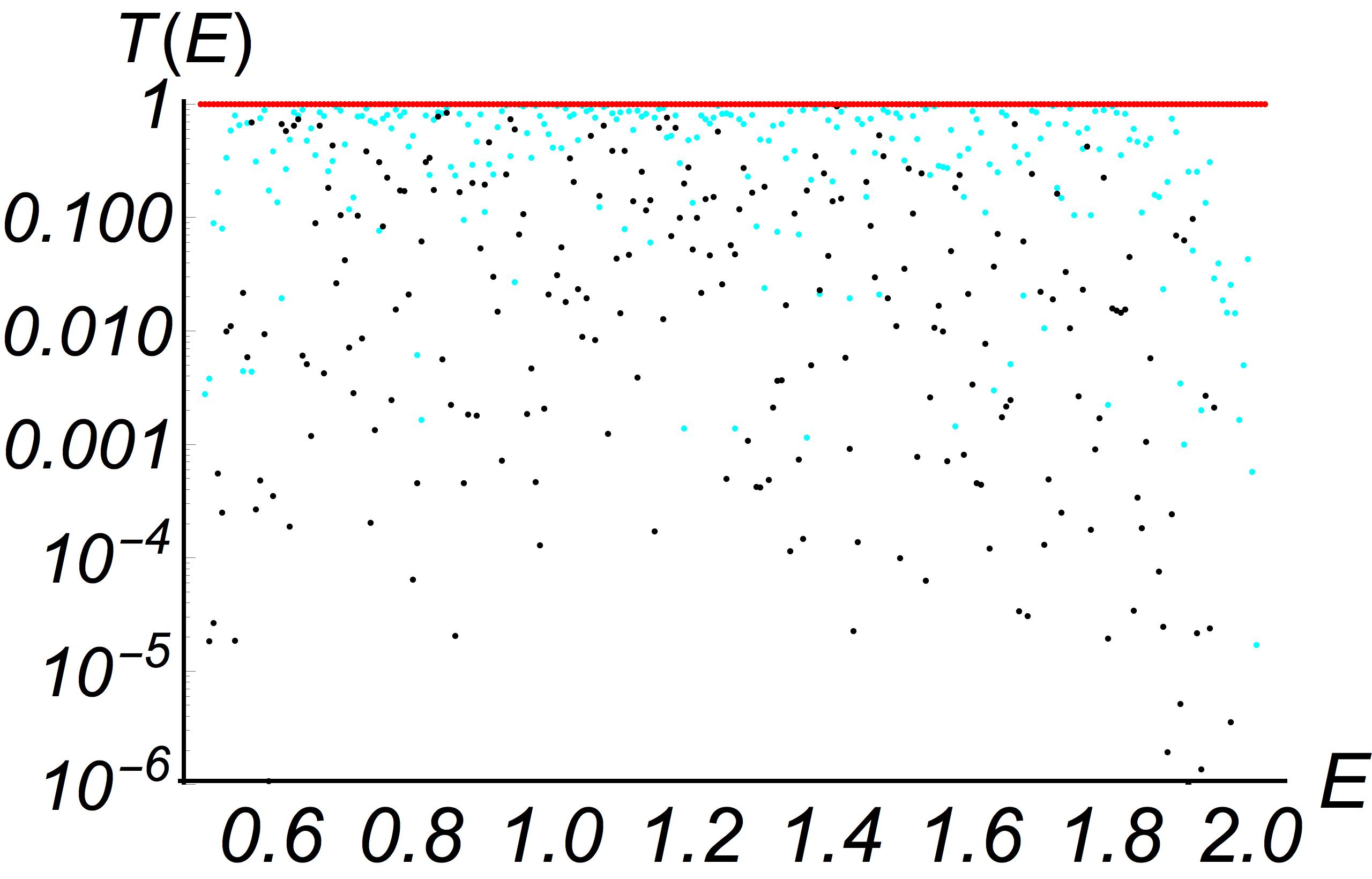
IV Numerical calculation of uniform quantum dragons
Here we provide a numerical example to illustrate the concept of quantum dragons for uniform leads,
based on the analysis in the previous section. The nanodevice can be viewed as related to the one in
Fig. 2, except for larger and values.
Our numerical results are shown in Fig. 3.
Any distribution for picking the random TB parameters is allowed.
For Fig. 3 the intra-slice terms, , were
uniformly distributed between and in this section we set .
Then we set all on site energies of the atoms in slice to be given by
Eq. (14).
The top plot in Fig. 3 shows our explicit values
for (blue circles) and (orange circles).
In order to keep all hopping strengths real and positive, since we are studying devices
in zero magnetic field, for the inter-slice TB parameters for every slice
we choose two random numbers and uniformly distributed in
and then to satisfy Eq. (15) choose the
inter-slice hopping strengths to be
In Fig. 3, 251 energies equally distributed between
were calculated. There are singularities present at
the lead band edges at , so these were avoided.
For every energy the matrix , with the same structure
as the matrix in Eq. (4), was numerically inverted.
Since the matrix is of dimension .
As expected for the quantum dragon system, in Fig. 3 we
see for all (red circles, which run together
so they seem to form a line segment).
We also wanted to see how behaves when we move away from the
condition of correlated disorder. For uncorrelated disorder, due to Anderson
localization ANDE1958 ; SCHW2007 , we expect very small for almost all
energies for a finite device size (finite ).
Therefore we also calculated for the case where to the on site
energy we added a small uncorrelated random value which is different
for all atoms in the nanodevice. Explicitly, we chose a random variate
from a normal distribution of mean zero and standard deviation unity, and then multiply by
a strength . The same random numbers were used for all values of studied.
Note if no exact mapping onto an equivalent 1D system is known.
Figure 3 shows results for the three values
(a quantum dragon, red points), (cyan points),
and (blue points). As expected for the transmission is
almost always small due to Anderson localization,
and is typically smaller for larger values of .
Note the logarithmic scale in Fig. 3 for ,
so the device has become an insulator for , while it is a quantum
dragon with a perfectly conducting channel for .
Figure 3:
(Color online.)
An example of uniform leads connected to a disordered, rectangular nanodevice
with and .
(Top) The correlated random values for slice for (blue circles)
and (orange squares).
(Middle) The correlated random values between slices numbered and
for (blue circles) and (orange squares).
(Bottom) Transmission as a function of energy for the disorder in the two upper
graphs (red), showing the quantum dragon condition . The three
values shown are (red) for correlated disorder only, and
for added on site uncorrelated disorder of strength
(cyan) and (blue).
V Discussion and conclusions
We have found the quantum dragon property, namely a perfectly conducting channel,
, for nanostructures based on rectangular graphs. The graphs
have open boundary conditions, with two sides connected to semi-infinite leads.
The hopping is nn, and between slices nnn hopping is also included. For no disorder,
the graphs become a rectangular crystal, and band structure properties can be
determined. When there is strong disorder, as in Fig. 2
and Fig. 6, band structure is ill defined. Nevertheless, even though
there is arbitrarily strong scattering, for all energies which propagate
through the leads. Hence quantum dragon nanodevices can be based on
rectangular graphs. For the quantum dragon nanodevices, because ,
the electrical conductance will be in two terminal and
in four terminal measurements. Furthermore, the shot power noise is .
The existence of quantum dragon solutions for electron transmission is extremely relevant
because of
recent experimental single layer thick materials based on rectangular lattices which have
been recently synthesized, including monolayers of Fe ZHAO2014
and of CuO YIN2016 ; KANO2017 .
Future work includes finding quantum dragons for different boundary conditions of
the underlying rectangular lattices.
Some of these were included in a recent Ph.D. dissertation INKO2017 .
In order to find quantum dragons with strong disorder, the crucial idea is all
intra-slice and all inter-slice parts of the Hamiltonian must have a common
eigenvector, and furthermore this eigenvector must correspond to a physically
realizable connection to the leads. For nanodevices based on rectangular lattices,
this is possible for other boundary conditions INKO2017 .
These studies may benefit from renormalization group calculations for transport,
such as have been used for hierarchical lattices Hanoi2011 .
Other further work could be to study the even-odd structure of rectangular CuO lattices,
where experimentally even-numbered and odd-numbered slices have different
structures YIN2016 ; KANO2017 . One expects again quantum dragon solutions, because the
same type of even-odd structure was exploited in the study of quantum dragon solutions
in single walled carbon nanotubes MANdragon2014 .
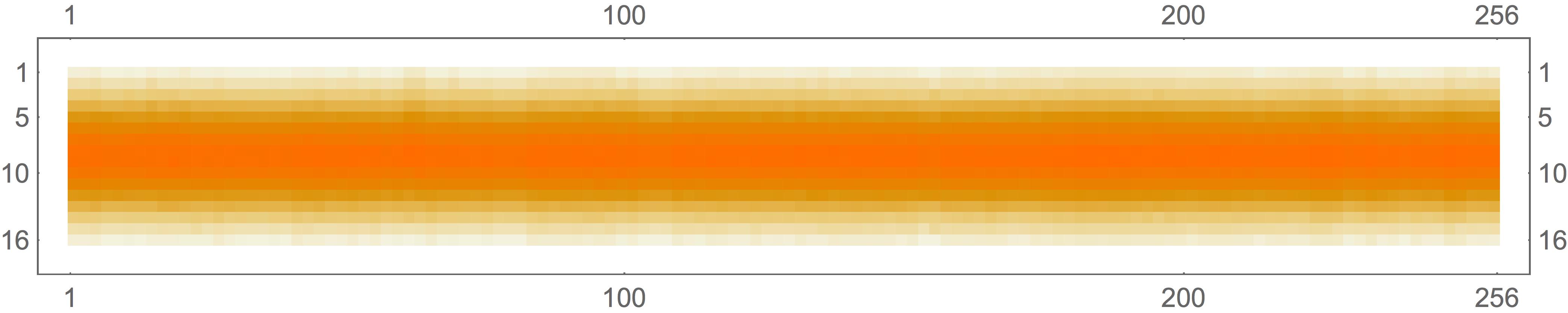
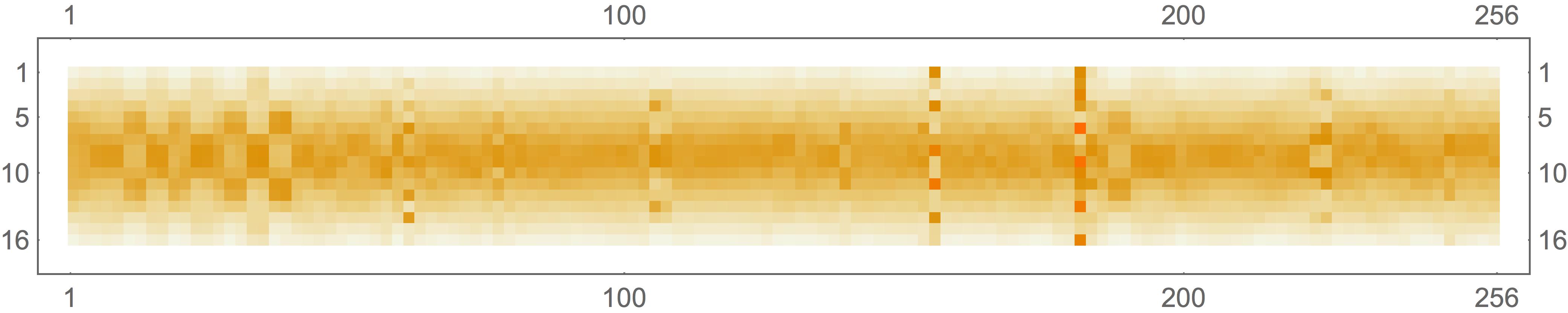
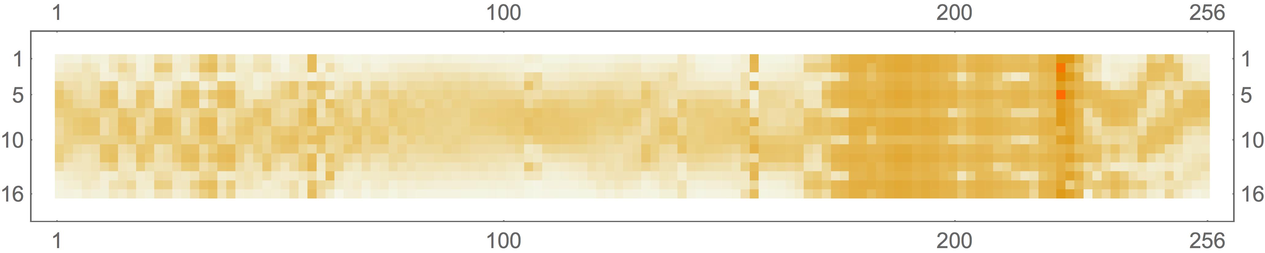
Further work can also be performed examining quantities such as a local density of states (LDOS).
The Green’s function is given in Eq. (59),
and the LDOS at is the imaginary part of the diagonal elements of
divided by SOUM2002 .
For a quantum dragon, as shown in
Fig. 4, the correlated disorder of a quantum dragon gives a LDOS
independent of the slice index , even though the disorder on every slice
is different.
Figure 4:
(Color online.)
The local density of states (LDOS) for a strongly disordered
nanodevice based on a rectangular lattice with
and , attached to uniform leads.
The correlated disorder in the TB parameters
, , , and is similar to
Fig. 3.
These are calculated with , but the results are similar for other energies.
The color coding has a larger LDOS for brighter, more orange pixels.
(Top)
The LDOS is independent of the slice when there is only correlated disorder,
so the device is a quantum dragon. Even though there is strong scattering, .
(Middle) With added uncorrelated on site disorder of strength the LDOS changes
dramatically, while the transmission decreases to .
(Bottom) The LDOS changes even more when for the same uncorrelated on site random disorder the
strength is , while the transmission has further decreased to
.
A further investigation of added disorder near a quantum dragon solution is also
warranted. We have observed such an analysis will require the study of the Fano
resonances MIRO2010 present, which are a source of the small values for electron
transmission seen in Fig. 3 and 7.
The full counting statistics of nanodevices FLIN2008 nearby in parameter space
to quantum dragon solutions would also be of interest.
One could also investigate how such quantum dragon solutions behave if one goes beyond
the TB model, for example using an exact discretization of the Schrödinger
equation TARA2016 , or due to many-electron effects such as were used recently
to analyze transport through a nanoscale ring-dot device BIBO2016 .
The possibility of technologically using quantum dragon solutions for field effect transistors
or sensors MANpatent also deserves further explaination. Furthermore, the possibilities
exist related dragon solutions may also be present in other strongly disordered systems,
for example where the open boundary conditions and disorder would normally lead to transverse
Anderson localization SCHW2007 in optical waveguides.
Acknowledgements
One of the authors (MAN) thank Tomáš Novotný and Maciej Maśka for useful discussions,
and the Faculty of Mathematics and Physics at
Charles University in Prague, Czech Republic for hospitality during
a stay as a Fulbright Distinguished Chair. Funding for MAN as a Fulbright Distinguished Chair
is gratefully acknowledged.
Appendix A: FOR FIGURES WITHOUT DISORDER
The complete description of two figures of the device and leads
without disorder, namely Fig. 1 and
Fig. 5 are given.
An example of the case of uniform (non-dimerized) leads, and no disorder in a rectangular lattice
device is shown in Fig. 1.
Because of the lack of disorder, the device can be considered to be a planar, rectangular crystal.
The location of the device is highlighted in light yellow.
The vertical gray lines show the division into slices, both for the device and
for the lead atoms.
Here there are slices in the device, and atoms in each slice.
Therefore, the device has atoms (red spheres).
The intra-slice hopping terms are shown by the vertical line segments
(green), TB parameters for slice , and are only between nn atoms.
The inter-slice hopping terms are for nn interactions shown by the
horizontal line segments (red-orange, TB parameter ),
and the nnn interactions shown by the
(black, TB parameter ) line segments which form an X-shape.
Only four atoms (blue-green) for both the incoming and outgoing semi-infinite leads are shown.
The connections between the leads and the device are shown by line segments (cyan)
with the width proportional to the elements of the eigenvector in Eq. (11).
Fig. 5 shows
an example of the case of dimerized leads and a dimerized device,
for no disorder in the rectangular device.
Consequently, the device may be considered to be planar.
The device is highlighted in light yellow.
The vertical gray lines show the division into slices, both for the device and
for the lead atoms.
Here there are slices in the device, and atoms in each slice.
Therefore, the device has atoms, denoted by different sized (and colored)
spheres for the odd slices (red) and even slices (green).
The different colors and sizes represent different values for the TB on site energies .
The first (leftmost) slice is numbered one.
The intra-slice hopping terms are only between nn atoms, and
are shown by the vertical line segments which are thick and green for the
odd-numbered slices and thinner and yellow for the even-numbered slices, representing TB parameters .
The inter-slice hopping terms are for nn interactions shown by the
horizontal line segments (magenta for odd-to-even and
yellow for even-to odd, representing TB parameters ), and the nnn interactions shown by the
line segments which form an X-shape (magenta for odd-to-even and
black for even-to-odd, representing the TB parameters ).
Only five atoms for the incoming lead and four atoms for the outgoing semi-infinite lead are shown
(large and fuchsia colored for odd-numbered atoms, while small and black for
even-numbered atoms, representing and TB parameters, respectively).
The lead hopping interactions are shown as thick (white) cylinders for
odd-to-even hopping terms (representing TB parameters ), and
thinner (yellow) cylinders for even-to-odd hopping terms (representing TB parameters ).
The connections between the leads and the device are shown by line segments
(cyan for the incoming lead, and magenta for the outgoing lead)
with the cylinder width proportional to the elements of the eigenvector in
Eq. (11).
Appendix B: FIGURES WITH DISORDER
The description for Fig. 2 and Fig. 6 is presented.
Consider a model where atoms in slice must be the same distance apart, as in a
ball-and-stick polymer model.
Hence, between nn atoms within slice there is only a single
distance allowed between the atoms (equivalent to attachment of springs with
infinite spring constant and equilibrium
distance ).
Between atoms in two neighboring slices, there are nn and nnn
equilibrium spring distances.
Let the hard spheres in slice be of radius .
Follow Konishi, et al Koni2008 for the Monte Carlo simulations and
energy functions.
The nn elastic interactions are
(18)
since all distances must be the same between the
intra-slice nn atoms. Here
(19)
is the distance (with the atoms confined to have the same value (with the
value the direction along which current will flow).
Here the index labels the atoms in the slice labeled .
This distance must be the same
between nn for all atoms in slices and , and consequently, they must have the same value of
and .
Similarly, the nnn elastic term is
(20)
with
(21)
We assume the hard sphere radii (the radii of the plotted spheres in the figures) is proportional to
for slice , namely .
We assume the distance between atoms within a slice has , with also reflected
by the radii of the cylinders representing the intra-slice bonds in the figures.
We assume the spring constants between slices have
and , and also the
width of the cylinders
representing the bonds have the same proportionality. One then has a complete (classical)
Hamiltonian for the nanosystems we study. The configuration of the classical representation of the
nanodevice is then found by perfoming a simulated annealing Monte Carlo process to attempt to
minimize the total elastic energy of the nanodevice.
Figure 2 contains an example of a nanodevice with uniform
(non-dimerized) leads. The device has slices, and atoms in every slice.
The underlying graph is rectangular, with nn interactions and also with nnn interactions
between atoms in neighboring slices.
Only five atoms in both the incoming and outgoing semi-infinite leads are shown.
The radii of the spheres are proportional to , and the radii of the
cylinders representing the bonds are proportional to the hopping strengths.
The bonds are magenta for nnn bonds (TB parameter for slice ),
cyan for nn inter-slice bonds (TB ), and green for nn
intra-slice bonds (TB ).
The are different for every slice,
and were chosen to be uniformly distributed in .
The on site energies of slice are all the same, with the given by the
quantum dragon condition of Eq. (14).
The inter-slice bonds are also all different, with the and
chosen to satisfy the quantum dragon condition of Eq. (15).
The connections between the leads and the device, blue-green cylinders, have strengths
given by Eq. (16).
Note the extreme disorder in the system, and that it is very far from a rectangular crystal,
rather it is a structure based on a rectangular graph. Nevertheless, for transmission it
has .
Figure 6 contains an example of a nanodevice with dimerized leads.
The device has slices, and atoms in every slice.
The underlying graph is rectangular, with nn interactions and also with nnn interactions.
Only five atoms in both the incoming and outgoing semi-infinite leads are shown,
with different colors and radii reflecting different on site energies,
(pink) and (black). The hopping terms in the leads
are also dimerized, representing (cyan, thick cylinder, smaller lattice spacing) and
(pink, thin cylinder, larger lattice spacing).
The radii of the spheres in the nanodevice are proportional to ,
with atoms red for odd-numbered and black for even-numbered .
The radii of the
cylinders representing the bonds are proportional to the hopping strengths.
The nnn bonds form an X-shape (TB parameter for slice , magenta for odd ,
cyan for even ).
The nn inter-slice bonds, TB , are also magenta for odd and
cyan for even .
The nn intra-slice bonds, TB , are green for odd and yellow for even.
The are different for every slice,
and were chosen to be uniformly distributed in () for
odd (even) .
The on site energies of slice are all the same, with the given by the
quantum dragon condition of Eq. (47).
The inter-slice bonds are also all different, with the and
chosen to satisfy the quantum dragon condition of Eq. (49)
and Eq. (50).
The connections between the leads and the device, blue-green cylinders, have strengths
proportional to with strengths given by the dragon condition
in Eq. (45).
Note the extreme disorder in the system, and that it is very far from a rectangular crystal,
being rather based on a rectangular graph. Nevertheless, for transmission it
is a quantum dragon with for all energies that propagate in the leads.
Appendix C: Derivation of matrix method for dimerized leads
In this appendix, an outline of the derivation for the transmission via the matrix
method is given.
This parallels Appendix A of ref. MANdragon2014, , with the exception here different
on site energies for the dimerized leads are also included.
This parallels the case of uniform leads DCA2000 , which is also
derived in the supplemental material of the 2014 quantum dragon paper MANdragon2014 .
For uniform leads the matrix form in the main text is obtained from results in this
section.
,
Figure 5:
(Color online.)
An example of dimerized leads connected to a
dimerized rectangular device, both without disorder.
See Appendix A.2 for a complete description.
Consider a nanodevice with atoms in every slice and with slices, connected
to dimerized leads, with an example shown in Fig. 5.
The leads (both incoming and outgoing) have on site energy
() for even (odd) numbered sites. The arrangement, including numbering
of the lead atoms, is as in the figure in Appendix A of ref. MANdragon2014, .
The outgoing lead is first completely analyzed, then the incoming lead is addressed. The
traveling-wave ansatz within the outgoing lead is the same as
Eq. [A3] of ref. MANdragon2014, (note equation numbers
from the 2014 paper MANdragon2014, are enclosed in square brackets)
(22)
The ansatz makes use of Bloch’s theorem
Bloch through the phase factor . Multiplying through
by the Hamiltonian of the outgoing lead becomes
(corresponding to Eq. [A4] of ref. MANdragon2014, )
(23)
which can be solved to eliminate to give (corresponding to Eq. [A5])
(24)
and using the double angle formula for gives
(25)
corresponding to Eq. [A6].
A propagating wave requires to be real, and hence or
for the two signs in front of the square root in Eq. (25).
One is free to set the zero for energy for the entire system, and a reasonable choice
is to set the zero at .
This can be accomplished by insisting
, with the zero of energy then at zero,
which is also
the midpoint between and .
This gives
propagating waves (corresponding to Eq. [A7]) for positive energies of
(26)
and
(27)
for negative energies.
By manipulating the two expressions in Eq. (23) one
finds
(28)
corresponding to Eq. [A8].
One also finds using the outgoing lead equations
as in Eq. [A10]
(29)
corresponding to Eq. [A12].
For the incoming lead one obtains
via the traveling-wave ansatz
(30)
which has all four terms in square brackets zero for
the expressions for in Eq. (28).
When , the values of are different for the
incoming () and outgoing () leads.
The incoming lead requires the association
(31)
with the further definition
(32)
Consequently, one obtains the solution to the transmission from the
solution to the matrix equation of the form (written for )
(33)
corresponding to Eq. [A11].
If one has ,
and therefore obtain the specialized case of Eq. (4).
The transmission is calculated by inverting the matrix for
a specific energy, and thereby obtaining .
For dimerized leads with and ,
has the form from Eq. [A8] and
consequently the energy range of propagating electrons is expressed as Eq. [A7].
For the case of uniform leads, with and
one has ,
In this appendix, the exact mapping as well as the locating of quantum dragons is
derived for the case of dimerized leads. We assume an underlying rectangular graph
with atoms placed on the nodes, and the graph is composed of slices each of
which have atoms.
An example for a rectangular crystal is shown in Fig. 5,
and an example based on an underlying rectangular graph, but with strong correlated
disorder is shown in Fig. 6.
Figure 6:
(Color online.)
An example of dimerized leads connected to a dimerized, disordered, rectangular device.
The same device is shown in the top (top view) and
bottom (oblique view) of the figure.
See Appendix B for a complete description.
The intra-slice parts of the device Hamiltonian, are
defined in Eq. (5).
The inter-slice parts of the device Hamiltonian, , are
defined in Eq. (6).
For our nanosystem based on an underlying rectangular graph, all and
are a sum of a constant times the identity matrix
plus another constant times
the matrix defined in Eq. (7).
The mutual eigenvector of all and is the vector
defined in Eq. (11).
Define a transformation matrix
(35)
where is a matrix, which can be thought of as being
composed of normalized vectors which are orthogonal to and
also are orthogonal to each other.
Therefore
and
.
Furthermore,
(36)
so
.
Next define a transformation matrix
of the form (written for )
(37)
which has the property .
Multiply the equations of the form of Eq. (33)
on the right by , and also
insert the identity
between the matrix and the vector containing the wavefunctions
at each site in the nanodevice. Written for , this gives
(38)
Because is an eigenvector of all
with eigenvalue in Eq. (13)
(39)
for some matrix
which will not enter into the calculation of .
Note we have defined .
Similarly, from Eq. (12) and
because is an eigenvector of
all , with eigenvalue , one has
(40)
with and where
is some matrix
which will not enter into the calculation of .
We also choose the connections to the nanodevice to be proportional
to , so
(41)
for some proportionality constants we label as and .
From Eq. (33) we can calculate the
transmission from the inverse of
the matrix as
(42)
However, with the transformation in Eq. (38)
a large part of the matrix is decoupled from both leads, namely the
parts which were labeled
and .
Therefore, we can also obtain the same transmission
from the inverse of the matrix
, which written for is
(43)
where
(44)
Eq. (44) is just the solution of a 1D chain of
atoms with on site energy and
nn (inter-slice) hopping strengths . Both the 2D system in Eq. (42)
and the 1D system in Eq. (44) have the same
transmission for all energies which propagate through the
semi-infinite leads. We have therefore completed our exact mapping for
the case of dimerized leads.
In order to find a quantum dragon, we need to find TB parameters which turn
the equivalent 1D mapped system of Eq. (44) into
a portion of length of the semi-infinite leads. This can be accomplished by
insisting that the original 2D device had TB parameters such that after mapping
we have the quantum dragon condition for the connections
(45)
where is the hopping strength in the leads from
even-numbered to odd-numbered atoms.
The quantum dragon conditions for the intra-slice parts of the Hamiltonian are
(46)
for . This can be satisfied by choosing the at random from any
distribution (keeping ), and then adjusting
(47)
which works since can be of either sign.
Therefore, the intra-slice nn hopping strength can be any random value,
provided one insists the satisfy Eq. (47).
For the inter-slice terms of the Hamiltonian, the quantum dragon condition becomes
(48)
for . However, we want to keep the tuned values of
and both positive, and remember both and
are positive. The negative signs for the hopping terms
have been put into the calculation by hand.
This can be accomplished by for each
choosing two random non-negative numbers and , and
setting the 2D device hopping to be
(49)
for odd and
(50)
for even. This completes the quantum dragon conditions, which when satisfied
gives for all energies which propagate through the leads.
Figure 7:
(Color online.)
An example of dimerized leads connected to a disordered, rectangular nanodevice
with and .
Transmission as a function of energy for the correlated disorder (red),
showing the quantum dragon condition . The three
values shown have correlated disorder so (red dots),
and added on site uncorrelated disorder of strength
(cyan dots) and (blue dots). See the text for a full description.
Fig. 7 is an example of a quantum dragon with
dimerized leads and a dimerized device. The device has slices each with
atoms. The leads have and together with
lead on site energies and (remember we have
set our zero of energy at the midpoint between the on site energies of the even and odd
numbered leads).
For these leads, from Eq. (26) and (27),
the leads allow electron transmission for energies in the ranges
and
. Only the positive energy
range is shown in Fig. 7.
Although any distribution of intra-slice hopping could be used, here
the were chosen uniformly in for even numbered slices and
in in odd numbered slices. Then the on site energy was set to the
quantum dragon condition in Eq. (47).
Similarly for the inter-slice hopping the
and were taken to be uniformly distributed in
for even and
in for odd , and then tuned to the quantum dragon
conditions as in Eq. (49) for odd
and Eq. (50) for even.
A total of 251 different energies uniformly spaced between
and were calculated.
Figure 7 shows for the quantum dragon condition
for the TB parameters all
energies have (red dots, which overlap to look like a line segment).
Additional uncorrelated random disorder was also included, every site having
a different on site added disorder found by choosing a random variant from a
normal distribution of mean zero and standard deviation unity, and then multiplying by a
value .
Figure 7 also shows the, usually very small,
values for obtained for (cyan dots) and
(blue dots).
Appendix E: Relationship between matrix and Green’s function methods
The relationship for dimerized single-channel leads, between the traditional
Green’s function method
DATTA1995 ; FerryGoodnick1997 ; TODO2002 ; DATTA2005 ; ZIMB2011 ; CUEV2017 ; TRIO2016
of solution and the matrix method of solution of the
time-independent Schrödinger equation is presented. The
leads have possibility for dimerized hopping ( and ) and dimerized
on site energies ( and ).
The matrix method for dimerized leads, related to Eq. (4), has the
general form
(51)
and requires one to find the inverse of the matrix
in order to find .
The transmission for any is then easily calculated by
.
The matrix in Eq. (51) is not Hermitian,
even for uniform leads due to the and
factors. The matrix is the Hamiltonian of
the nanodevice, and is therefore Hermitian.
Any block-tridiagonal matrix of the form above
has an inverse matrix that can easily be written as
(52)
with the definition
(53)
This gives
,
which is useful in showing Eq. (52).
Therefore, we have calculated the inverse of the matrix in
Eq. (51), namely the matrix on the left in Eq. (52).
Multiplying through in Eq. (51) by the matrix inverse, one obtains
(54)
and consequently the transmission is
(55)
In the case of uniform leads the on site energies and are set to zero,
giving the zero of energy.
Furthermore, for uniform leads , setting the unit of energy.
Then
and and , as well as
, giving the transmission
Therefore, we only need to show to complete the equivalence between the Green’s function
and matrix methods that
.
This is shown via
(63)
where use has been made of
.
In addition, one has
(64)
where use has been made of
(65)
and the double angle formula
(66)
Consequently we have shown
(67)
Therefore, in the general case within the TB model,
we find the matrix method to obtain from
Eq. (51) for both dimerized leads and uniform leads
to be equivalent to the Green’s function method which has
(68)
Appendix F: Quantum dragon solution for
The full solution is presented for dimerized leads connected to a simple two-slice (,
) device. The same equations for the transmission are
also valid for uniform leads attached to an device.
For simplicity, we take , setting our zero of energy
in the problem.
This also means for both the incoming and outgoing leads .
The Green’s function method is used, thereby requiring
only use of matrices. The goal of this section is to show the full solution
for the transmission for the general case, and show how it simplifies to the
quantum dragon solution .
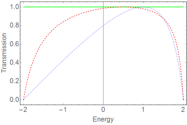
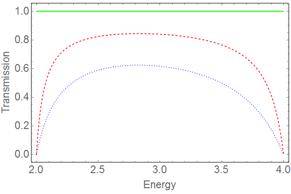
Figure 8:
(Color online.)
Transmission vs energy for devices with
and .
(Top) Uniform leads. In all three curves .
Shown are the three cases (blue, dotted),
(red, dashed), and the quantum
dragon solution (green, solid).
(Bottom) Dimerized leads with and , and
all curves have .
Shown are the same three cases as in the top graph, namely
(blue, dotted),
(red, dashed), and the quantum
dragon solution (green, solid)
of for all energies which propagate in the
leads.
See text in Appendix E for a complete description.
The Hamiltonian for the simple 2 site (, ) device is
(69)
with hopping between the two atoms in the device, and on site
energies for the two atoms and .
The device is coupled to two dimerized single-channel leads [incoming
vector and outgoing
vector ],
giving the self energy matrices
(70)
The figure setup is the same as in App. A of ref. MANdragon2014, .
It should be noted that the quantity is complex, but both and are
here taken to be real positive numbers.
The complex quantity is different for uniform leads and dimerized leads,
namely
(71)
From Eq.(70), the coupling matrices are expressed as
(72)
and
(73)
The Green’s function, is
(74)
with and .
The electron transmission probability can be expressed in terms of the Green’s function,
and the coupling matrices, and as
(75)
Put Eq. (72), Eq. (73) and
Eq. (74) into Eq.(75).
This gives the electron transmission probability as
Eq. (77) is the transmission probability for the two site device coupled to
either uniform () or dimerized ()
leads, depending on the value of
in Eq. (71)
and in Eq. (32).
A plot of
for for selected parameters is shown in Fig. 8 for both
uniform and for dimerized leads.
To see how the quantum dragon solution is obtained from the mathematics, consider a
and device with uniform leads (), with
and
so .
Eq. (78) gives the quantum dragon solution from the operations
(79)
This and device acts as a ‘short circuit’ between the
two uniform leads.
Because it is a
‘short circuit’, physically the solution makes
sense. This physical solution should also extend to the
case of and general , but the algebra becomes
more messy than Eq. (79).
Starting from Eq. (78) for the dimerized case, a ‘short circuit’ should
be found for even when , , and
. However, the algebra becomes very messy
in this case, even for a and device.
However, physically one expects a ‘short circuit’ solution
in the quantum sense, because the inserted device
has the same structure as the leads. This is indeed what we observe numerically,
as seen in Fig. 8.
References
(1) M.M. Waldrop,
The chips are down for Moore’s law,
Nature 530, 141-147 (2016).
(2) T. Tsurumi, H. Hirayama, M. Vacha, and T. Taniyama,
Nanoscale physics for materials science
(CRC Press, Boca Raton, FL, 2010).
(3)Nanoelectronics: Materials, Devices, Applications, two volumes,
Edited by R. Puers, L. Baldi, M. van de Voorde, and S.E. van Nooten,
(Wiley-VCH, Weinheim, Germany, 2017).
(4)
Datta, S. Electronic Transport in Mesoscopic Systems
(Cambridge University Press, Cambridge, UK, 1995).
(5)
Ferry, D.K., & Goodnick, S.M. Transport in Nanostructures
(Cambridge University Press, Cambridge, UK, 1997).
(6) T.N. Todorov,
Tight-binding simulation of current-carrying nanostructures
J. Phys.: Condens. Matter 14, 3049-3084 (2002).
(7)
Datta, S. Quantum Transport: Atom to Transistor
(Cambridge University Press, Cambridge, UK, 2005).
(8)
N.A. Zimbovskaya and M.R. Pederson,
Electron transport through molecular junctions,
Phys. Reports 509, 1-87 (2011).
(9)
J.C. Cuevas and E. Scheer,
Molecular Electronics: An introduction to theory and experiment,
edition,
(World Scientific, Singapore, 2017).
(10)
Landauer, R. Spatial variation of currents and fields due to localized scatterers in
metallic conduction.IBM J. Research and Development1, 223-231 (1957).
(11)
P.F. Bagwell and T.P. Orlando,
Landauer’s conductance formula and its generalization to finite voltages.Phys. Rev. B40, 1456-1464 (1989).
(12) G.B. Lesovik,
Excess quantum noise in 2D ballistic point contacts,
JETP Lett. 49, 592-594 (1989).
(13) M. Büttiker,
Scattering theory of thermal and excess noise in open conductors,
Phys. Rev. Lett. 65, 2901-2904 (1990).
(14)
A. Kumar, L. Saminadayar, D.C. Glatti, Y. Jin, and B. Etienne,
Experimental test of the quantum shot noise reduction theory,
Phys. Rev. Lett. 76, 2778-2781 (1996).
(15)
T. Ouisse, Electron Transport in Nanostructures and Mesoscopic Devices: An Introduction
(John Wiley & Sons, Hoboken, NJ, 2013).
(16)
R. de Picciotto, H.L. Stormer, L.N. Pfeiffer, K.W. Baldwin, and K.W. West,
Four-terminal resistance of a ballistic quantum wire,
Nature 411, 51-54 (2001).
(17) K. Wakabayashi, Y. Takane, and M. Sigrist,
Perfectly conducting channel and universality crossover in disordered graphene
nanoribbons, Phys. Rev. Lett. 99, 036601 (2007).
(18) A. Matsumoto, T. Arita, Y. Takane,
Y. Yoshimura, and K.-I. Imura,
Manipulating quantum channels in weak topological insulator nanoarchitectures,
Phys. Rev. B 92, 195424 [14 pages] (2015).
(19)
M.A. Novotny, Energy-independent total quantum transmission of
electrons through nanodevices with correlated disorder,
Phys. Rev. B 90, 165103 [14 pages] (2014).
(20) M. Ouyang, J.-L. Huang, C.L. Cheung, and C.M. Lieber,
Energy gaps in “metallic” single-walled carbon nanotubes,
Science 292, 702-702 (2001).
(21)
J. Kong, E. Yenilmez, T.W. Tombler, W. Kim, and H. Dai,
Quantum interference and ballistic transmission in nanotube electron waveguides,
Phys. Rev. Lett. 87, 106801 [4 pages] (2001).
(22) J. Baringhaus, M. Ruan, F. Edler, A. Tejeda, M. Sicot, A. Taleb-Ibrahim,
A.-P. Li, Z. Jiang, E.H. Conrad, C. Berger, C. Tegenkamp, and W.A. de Heer,
Exceptional ballistic transport in epitaxial graphene nanoribbons,
Nature 506, 349-354 (2014).
(23) A. Celis, M.N. Nair, A. Taleb-Ibrahim,
E.H. Conrad, C. Berger, W.A. de Heer, and A. Tejeda,
Graphene nanoribbons: fabrication properties and devices,
J. Phys. D: App. Phys. 49, 143001 (2016).
(24) C.T. White and T.N. Todorov,
Carbon nanotubes as long ballistic conductors,
Nature 393, 240-242 (1989).
(25)
D. Erts, H. Olin, L. Ryen, E. Olsson,
and A. Thölén,
Maxwell and Sharvin conductance in gold point contacts investigated using TEM-STM
Phys. Rev. B 61, 112725-12727 (2000).
(26)
Daboul, D., Chang, I., & Aharony, A. Series expansion study of quantum percolation on the square lattice.
Euro. J. Phys. B16, 303-316 (2000).
(27) J. Zhao, Q. Deng, A. Bachmatiuk, G. Sandeep, A. Popov, and J. Eckert,
Free-standing single-atom thick iron membranes suspended in graphene pores,
Science 343, 1228-1232 (2014).
(28) K. Yin, Y.-Y. Zhang, Y. Zhou, L. Sun, M.F. Chisholm,
S.T. Pantelides, and W. Zhou,
Unsupported single-atom-thick copper oxide monolayers,
2D Mater. 4, 011001 [8 pages] (2017).
(29)
E. Kano, D.G. Kvashnin, S. Sakai, L.A. Chernozatonskii,
P.B. Sorokin, A. Hashimoto, and M. Takeguchi,
One-atom-thick 2D copper oxide clusters on graphene,
Nanoscale 9, 3980-3985 (2017).
(30) K.S. Novoselov, A. Mishchenko, A. Carvalho, and A.H. Castro Neto,
2D materials and van der Waals heterostructures,
Science 353, aac9439 [11 pages] (2016).
(31)
S. Boettcher, C. Varghese, and M.A. Novotny,
Quantum transport through hierarchical structures,
Phys. Rev. E 83, 041106 [12 pages] (2011).
(32)
M.A. Novotny, L. Solomon, and G. Inkoom,
Quantum transport through a fully connected network with disorder,
Phys. Proceedia 53, 71-74 (2014).
(33)Simulation of transport in nanodevices,
Editors F. Triozon and P. Dollfus,
(John Wiley & Sons, Hoboken, NJ, 2016).
(34) A.K. Jain,
A sinusoidal family of unitary transforms,
IEEE Trans. Pattern Analysis and Machine Intelligence,
PAMI-1, 356-365 (1979).
(35) P.W. Anderson,
Absence of diffusion in certain random lattices,
Phys. Rev. 109, 1492-1505 (1958).
(36)
T. Schwartz, G. Bartal, S. Fishman, and M. Segev,
Transport and Anderson localization in disordered two-dimensional photonic lattices,
Nature 446, 52-55 (2007).
(37) G. Inkoom,
Quantum dragon solutions for electron transport through single-layer planar
rectangular crystals, Ph.D. Dissertation, Mississippi State University, 2017.
(38)
S. Boettcher, C. Varghese, and M.A. Novotny
Quantum transport through hierarchical structures
Phys. Rev. B 83, 041106 [12 pages] (2011).
(39)
S. Souma and A. Suzuki,
Local density of states and scattering matrix in quasi-one-dimensional systems,
Phys. Rev. B 65, 115307 [7 pages] (2002).
(40)
A.E. Miroshnichenko, S. Flach, and Y.S. Kivshar,
Fano resonances in nanoscale structures,
Rev. Mod. Phys. 82, 2257-2298 (2010).
(41) V.E. Tarasov,
Exact discretization of Schrödinger equation,
Physical Letters A 380, 68-75 (2016).
(42)
C. Flindt, T. Novotnyý, A. Braggio, M. Sassetti, and A.-P. Jauho,
Counting statistics of non-Markovian quantum stochastic processes,
Phys Rev. Lett. 100, 150601 [4 pages] (2008).
(43)
A. Biborski, A.P. Kadzzielawa, A. Gorzyca-Goraj, E. Zipper, M. Maśka, and J. Spalek,
Dot-ring nanostructure: Rigorous analysis of many-electron effects,
Scientific Reports 6, 29887 [14 pages] (2016).
(44) M.A. Novotny,
Materials and devices that provide total transmission of electrons without ballistic propagation and
methods for devising same, U.S. Patent Pending.
(45)
Y Konishi, H. Tokoro, M. Nishino,
and S. Miyashita,
Monte Carlo Simulation of Pressure-Induced Phase
Transitions in Spin-Crossover Materials
Phys. Rev. Lett. 100, 067206 [4 pages] (2008).
(46)
F. Bloch,
Über die Quantenmechanik der Electronen in Kristallgittern,
Z. Physik 52, 555-600 (1928).