Relaxation of a Mott-neuron
Abstract
We consider the phenomenon of electric Mott transition (EMT), which is an electric induced insulator to metal transition. Experimentally, it is observed that depending on the magnitude of the electric excitation the final state may show a short lived or a long lived resistance change. We extend a previous model for the EMT to include the effect of local structural distortions through an elastic energy term. We find that by strong electric pulsing the induced metastable phase may become further stabilized by the electro-elastic effect. We present a systematic study of the model by numerical simulations and compare the results to new experiments in Mott insulators of the AM4Q8 family. Our work significantly extends the scope of our recently introduced leaky-integrate-and-fire Mott-neuron [P. Stoliar Adv Mat 2017] to bring new insight on the physical mechanism of its relaxation. This is a key feature for future neuromorphic circuit implementations.
.1 Introduction
The information age we live in is supported on a physical under-layer of electronic hardware, which originates in condensed matter physics research. The mighty progress made in recent decades produced faster and more power efficient electronic devices. This enabled a seemingly endless improvement in computer performance. However, with the smallest feature size of transistors reaching down to mere 5 nm, the technology is reaching an unavoidable physical limit. This situation concerns the current computational paradigm, based on binary logic and the von Neumann architecture. While incremental progress along this direction is likely to go on, the search for disruptive technologies is on.
On the other hand, we are currently witnessing significant progress in artificial intelligence. In fact, older algorithmic paradigms, such as neural networks combined with newer ideas such as wavelet based filtering have produced a remarkable improvement of performance of computers at dealing with tasks where they were traditionally poor, such as pattern recognition. This area of research is known as Deep Neural NetworksMallat (2012); Schmidhuber (2015). However, most of this progress has been reached by running the new algorithms with conventional codes on conventional (i.e. von Neumann) computers. While the performance of these algorithms is remarkable at many tasks, unfortunately, it is limited by the computational power of current machines. For instance, the number of synapses in a brain is 1015, thus even if one allocates a single memory per synapse, conventional computers fall irreparably short.
Therefore, an exciting perspective is to implement the neural networks directly on hardware, by realizing novel electronic devices that may directly implement the neural network functionality. These bio-inspired electronic circuits have two key new components. One is an “synapse analogue” and the other is an “neuron analogue”. The former can be implemented by a non-volatile resistance, whose value can be programmed (and re-programmed) by application of voltage pulses. This can be effectively done by the so called RRAM devices (for resistive random access memories) and also known as memristors (for memory dependent resistors). One widely adopted implementation of these systems is in the form of capacitor-like structures, where the two electrodes are ordinary metals (Pt, Ti, etc) and the dielectric is a transition metal oxide Rozenberg (2011). The resistive change is observed in the two-terminal resistance of the device, which can be modified by electric pulsing Janod et al. (2015). These devices have been intensively investigated and developed during the past decade. The basic physical mechanisms for the resistive change in these oxide memristive devices are now understood in certain detail Wong et al. (2012). They are mainly based on achieving structural changes by inducing oxygen or metallic ion migration Tang et al. (2016). After more than a decade of intense research these type of devices are beginning to reach the market.
This significant progress enables the implementation of “synapses analogue” Jo et al. (2010); Pershin and Ventra (2010), unfortunately, the progress in the research and implementation of “neurons analogue” has not been comparable. Hence, their development becomes urgent.
In the context of resistive change systems we may mention two important contributions towards devices with a “neuron” inspired functionality: one is the “neuristor”, which realizes a functionality similar to the Hodgkin-Huxley model for electric pulse propagation in biological axons Pickett et al. (2013). The other one is the “artificial neuron”, which implements the functionality of a leaky-integrate-and-fire (LIF) biological spiking neuron Stoliar et al. (2017). Remarkably, both implementations are based on Mott insulators, which are strongly correlated systems that exhibit metal-insulator transitions Imada et al. (1998). Mott systems have been intensively investigated since the 80’s, following the discovery of high temperature superconductivity in cuprates. Their basic feature of Mott insulators is that according to their expected band-structure they should be metals, with partially filled bands, however, they turn out to be insulators. The physical reason is due to the effect of the strong local Coulomb repulsive interaction between electrons in -orbital bands that localize the electrons Imada et al. (1998).
Here we shall focus on the latter of those two types of artificial Mott neuron systems. More specifically, we shall gain insight in a key feature of the LIF model, namely the “leaky” property and shall also extend our model to study the recovery behavior of the Mott neuron right after the firing event which is corresponding to the “refractory period” of a biological neuron. In the LIF model, a neuron is excited by a train of incoming electric pulses (spikes), which are integrated in time by the neuron, until it reaches a threshold level where it fires a spike. The “fire” event in the Mott neuron corresponds to the EMT, that is the resistance collapse of the Mott insulator. The leaky property models the fact that in the “down” time in-between pulses the excitation level of the neuron slowly decays with a given relaxation time constant. Evidently, for a neuron to reach a threshold and fire, the time-delay between arriving pulses has to be shorter than the relaxation time constant of that neuron Stoliar et al. (2013). Therefore, the control of the “leaky time” is a key issue. On the other hand, the “refractory time” of a biological neuron refers to the period of time right after the fire event while the neuron cannot fire again. As we shall see below, in our artificial Mott neuron model both features are related to the same underlying mechanism, which leads to two characteristic relaxation times of the system.
One may naively expect that the relaxation time would be an intrinsic constant of the material, however the situation is more complex since the artificial neurons are based on strongly correlated Mott materials that undergo insulator-metal phase transitions. In systems in equilibrium, Mott transitions can be induced and controlled by a variety of parameters, such as pressure, chemical doping and temperature. However, in the present situation, the understanding of the relaxation is further complicated by the fact that the LIF functionality is a property of the system out-of-equilibrium. That is, when the Electric Mott Transition (EMT) is induced by pulses of electric field that provoke a partial dielectric breakdown. During this breakdown, the resistance collapses Guiot et al. (2013); Stoliar et al. (2013), and eventually recovers back to the original value after the application of the electric pulse is terminated. The theoretical understanding of the recovery of a Mott insulator from the collapsed resistance state is a challenging many-body out of equilibrium problem of actual interest Aoki et al. (2014).
Experiments of EMT show that the relaxation from the low to the high-resistance state of a Mott insulator depends significantly on the strength of the applied electric field Janod et al. (2015). In fact, the systematic study of the field induced dielectric breakdown in the Mott system GaTa4Se8 and similar compounds revealed the existence of three different regimes: (i) at low applied electric fields there is, of course, no large resistance change, (ii) at intermediate field strength there is a volatile change of resistance, that is, there is an initial sudden collapse followed by a recovery. And (iii) at high fields there is a seemingly non-volatile change of resistance, that is, the resistance collapses and does not recover or may take very long time (i.e., the retention time is virtually infinity). In our artificial neuron model, we associate the duration of the resistance recovery to the “refractory period” mentioned above, and its characteristic time will be termed retention time.
We should note that the resistive change in regime (ii) is a perfectly reproducible effect and the breakdown occurs after a delay-time (of the order of s to ms), strongly dependent on the applied voltage Janod et al. (2015). When the applied voltage pulse is terminated, the low resistance relaxes back to the original high value in a characteristic time that we shall denote Stoliar et al. (2017). In contrast, in regime (iii) the resistance change is permanent, i.e. , but the resistive changes are more difficult to control and reproduce. We should also note that we are discussing the resistance and not the resistivity. It is still not fully understood how the resistive transition occurs spatially. It is most likely through electronic filamentary structures formation Stoliar et al. (2013)
In previous works, we have introduced a model that accounts fairly well for the basic phenomenology of the EMT Stoliar et al. (2013). However, that model has a single relaxation time for the recovery of the “broken-down” metallic regions back to the initial Mott insulator state. This feature clearly cannot account for the observation of the regime (iii) described above, and neither to the behavior of with applied pulse strength in regime (ii) as is observed in the experiments that we shall report here. Thus, the main goal of the present work is to extend the previous model to capture the behavior of the relaxation time in the experiments of the EMT. We shall show that by introducing an electro-elastic effect, the relaxation time will display a non-trivial behavior. For instance, we shall show that the duration of the relaxation will depend on the volume fraction that has changed from Mott-insulator to metal during the application of the voltage pulses. Related to this and relevant for experiments, we shall see that by application of a higher voltage strength and/or a longer pulse duration one may induce the growth of thicker metallic filaments and achieve a significant increase of the relaxation time.
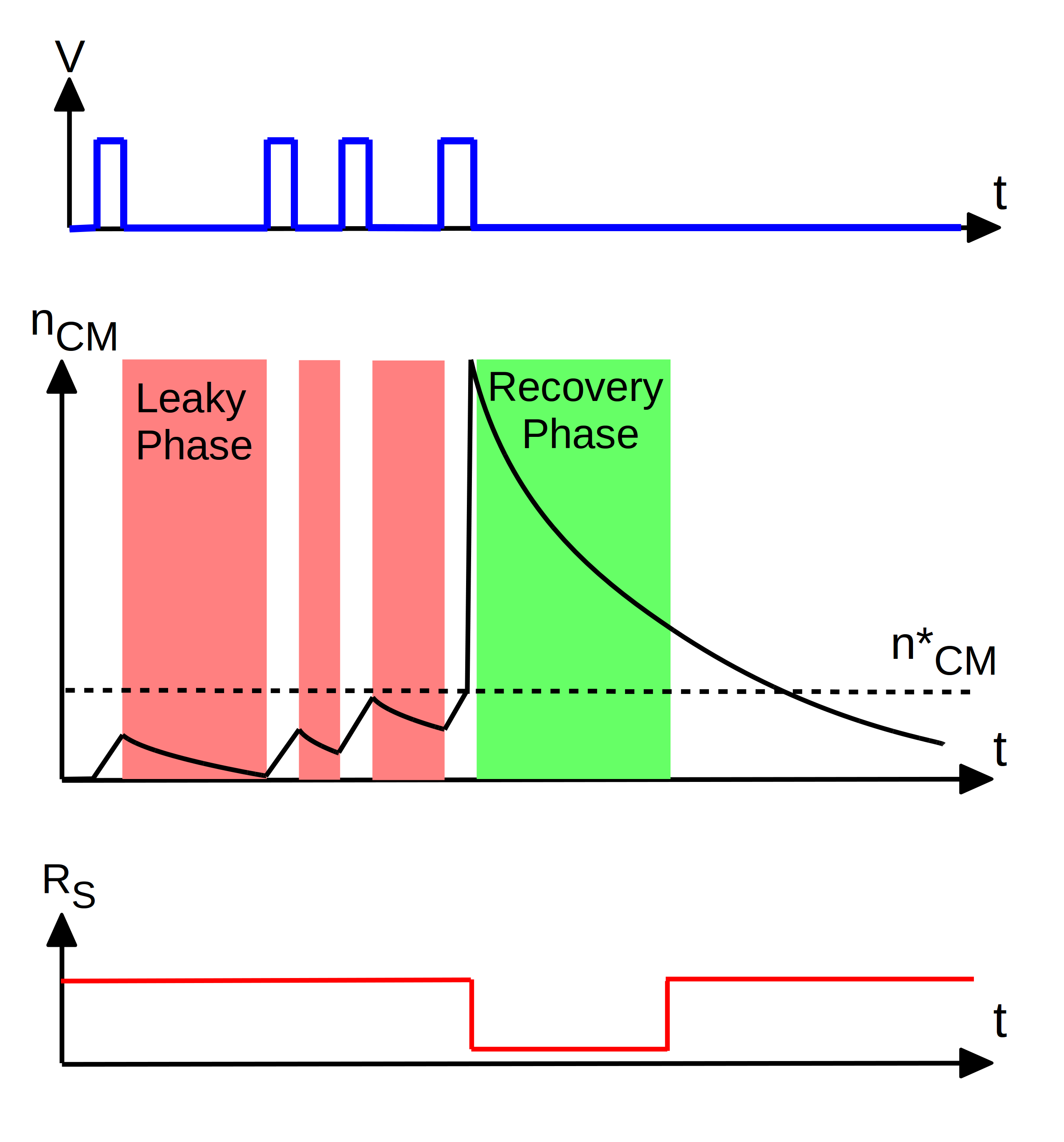
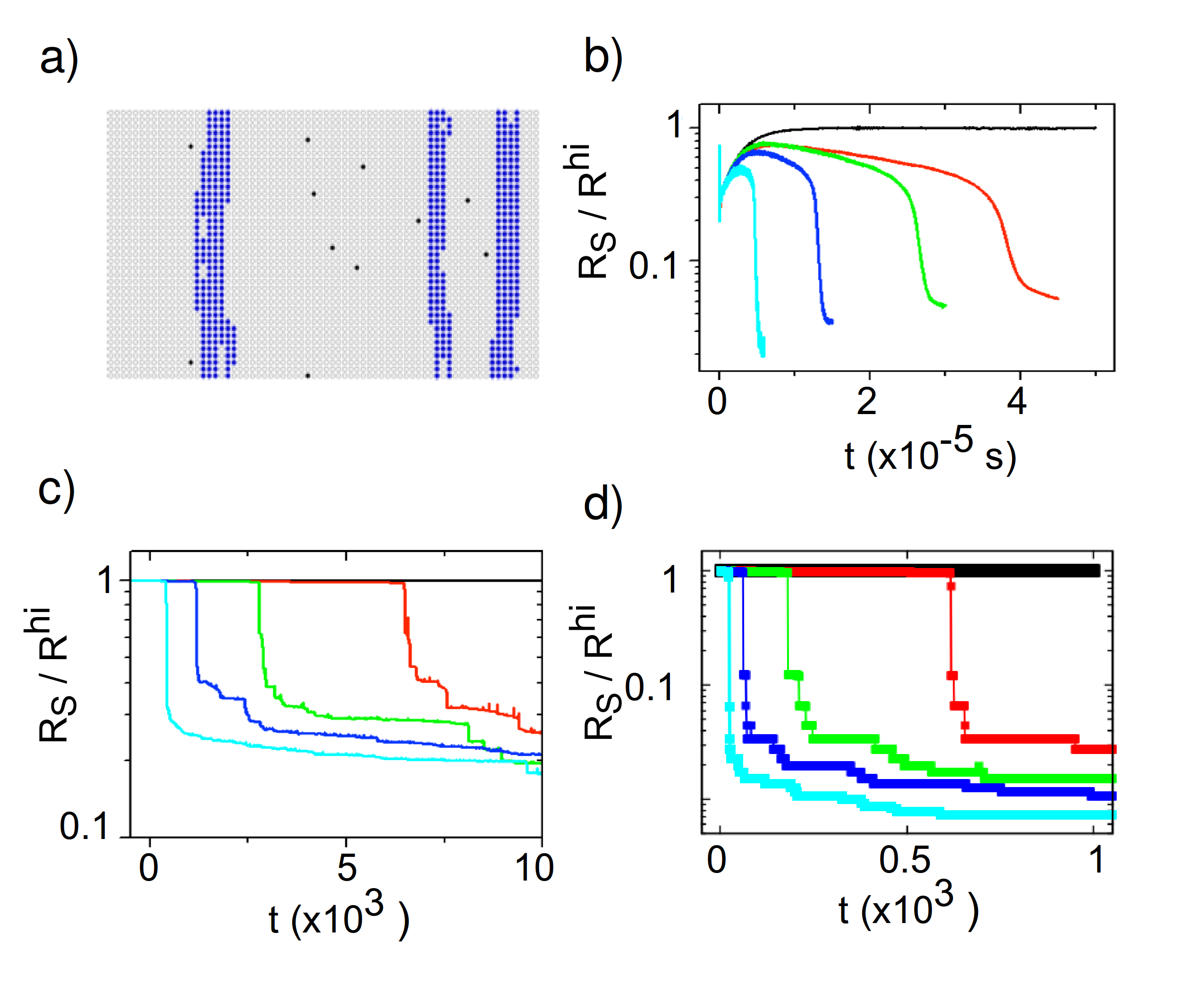
Before introducing the model we should clarify a few important points, which connect the present study to a model of a neuron analogue aimed at the implementation of bio-inspired neural networks. The resistive collapse is considered to result from a two-step process. The initial one where the strong applied field enhances the rate of phase change and a larger number of isolated small regions of the insulating material turn metallic. If the production rate is sufficiently large, more than the rate of relaxation of those regions back to the insulator state, then the density of metallic regions will steadily increase. Eventually it will reach a critical density where a sudden avalanche-like process will create a filament Stoliar et al. (2013). The resistance change during the first part of the process is quite small, and the collapse of its value is due to the formation of the filament or, if the applied voltage is strong, of more filaments at random positions, further reducing the resistance. That initial model assumed a single intrinsic time for the relaxation of metallic regions back to insulator state, irrespective of whether it belonged to an isolated region or was part of a filamentary structure. This feature will be partially modified in the model introduced in the present work. We shall make the additional assumption that the relaxation probability of a given cell depends on the current state of its neighboring cells. Hence, a metallic cell will effectively have a different relaxation rate depending whether it is an isolated one or it is within a filamentary structure. The model will aim to describe the whole process of resistance collapse and recovery, namely the filament formation and its reabsorption. The leaky-time of a neuron analogue model Stoliar et al. (2017) is associated to the dynamics of the neuron in between arriving pulses before the fire. Correspondingly, in the context of the present model, the leaky behavior is associated to the behavior of the system during the initial filamentary formation process. More specifically, with the initial stage where the density of isolated metallic regions increase until the critical density is attained and with the ensuing rapid growth of the filamentary structure. Experimentally, this leaky stage may be explored and characterized by the application of short electric pulses Stoliar et al. (2017). In contrast, there is a process of reabsorption of a formed filament, which corresponds to the resistance recovery from low to high, that begins when the pulse is terminated after the fire event (see Fig.1) This process is what one would associate to the “refractory-time” of a biological neuron. However, there is a significant difference between the refractory time of a biological neuron and the Mott neuron. In the former, the neuron is “off” during the refractory time, that is, arriving spikes cannot induce a new action potential. In the Mott neuron, in contrast, the system is in the low resistance state, which means that arriving pulses will generate current pulses. Because of this difference, we term the recovery of the high-resistance state (i.e. filament reabsorption and rupture) as “recovery time” instead of refractory time (see Fig. 1).
As we shall see from the study of the simulation results of our model, the leaky process corresponds to the relaxation of isolated metallic regions in an essentially insulating system, while the recovery period corresponds to the rupture or de-percolation process of already formed metallic filaments. We shall see that both the leaky and the recovery phases are captured by our model. As we shall also show in experiments that we report here, our modeling work provides useful insight for the control of these relevant neuronal model features.
.2 The model
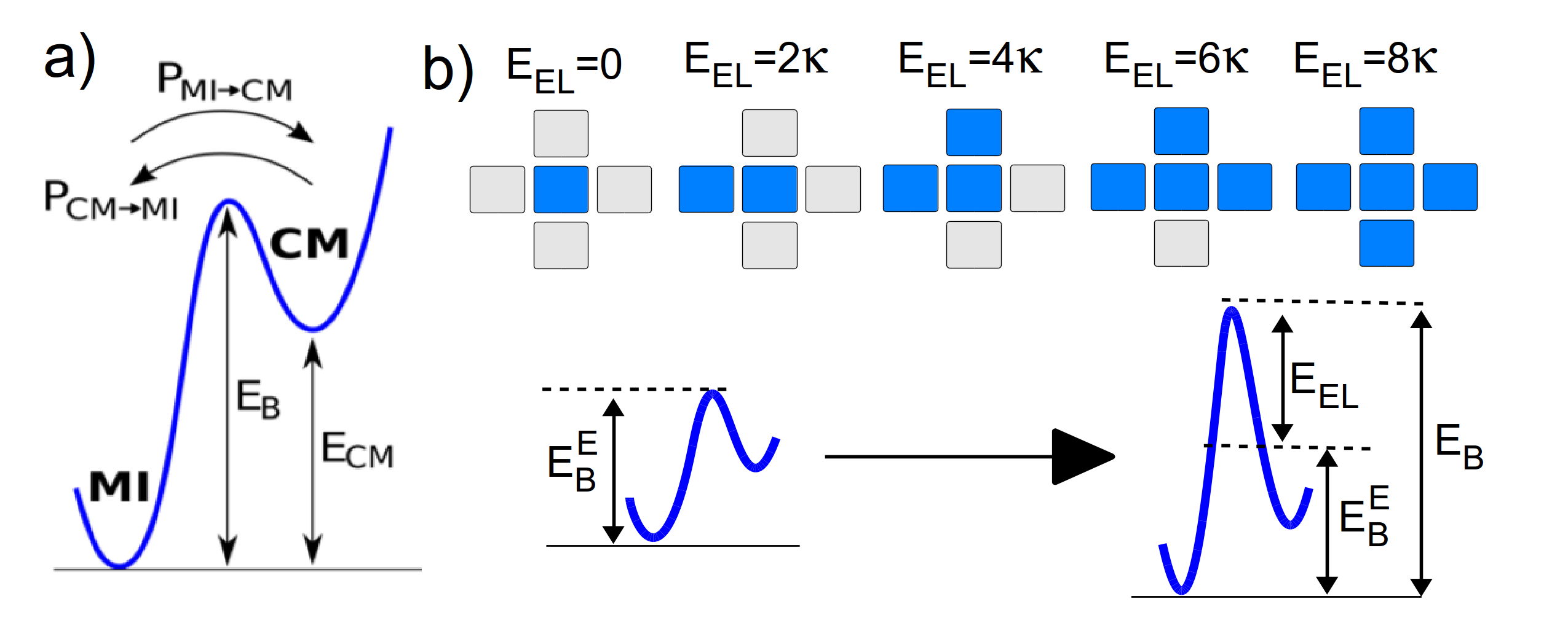
We start from the model introduced by Stoliar et al. Stoliar et al. (2013) that consists of a 2D resistor-network where each element of the network represents a small (nanoscale) region of the physical Mott system Stoliar et al. (2013, 2014). The cells of the network are assumed to be large enough so that its electronic state is well defined. Imaging technique experiments with nanoscale spatial resolution have shown that across the Mott transition there is a coexistence of metallic and insulating phases with inhomogeneous distributions down to the few nanometers Qazilbash et al. (2007); Dubost et al. (2013). Each cell site is assumed to be in one of two electronic states: Mott-insulator (MI) or correlated-metal (CM). These states are respectively associated with a high and a low resistance values, and . The resistor network model is schematically shown in Fig.2.a-b. Since the experimental systems are normally in the insulator state, the model assumes that the MI-state is the lowest in energy, which is defined as the reference . The CM-state is assumed to be a metastable state, with a higher energy , and separated from the MI-state by an energy barrier of pure electronic origin (see Fig.3.a). From Dynamical Mean Field Theory calculations of the Hubbard model for Mott systems Camjayi et al. (2014); Georges et al. (1996), one may expect that the energy difference between these states may be of the order of a few tens of , substantially smaller than the electronic bandwidth .
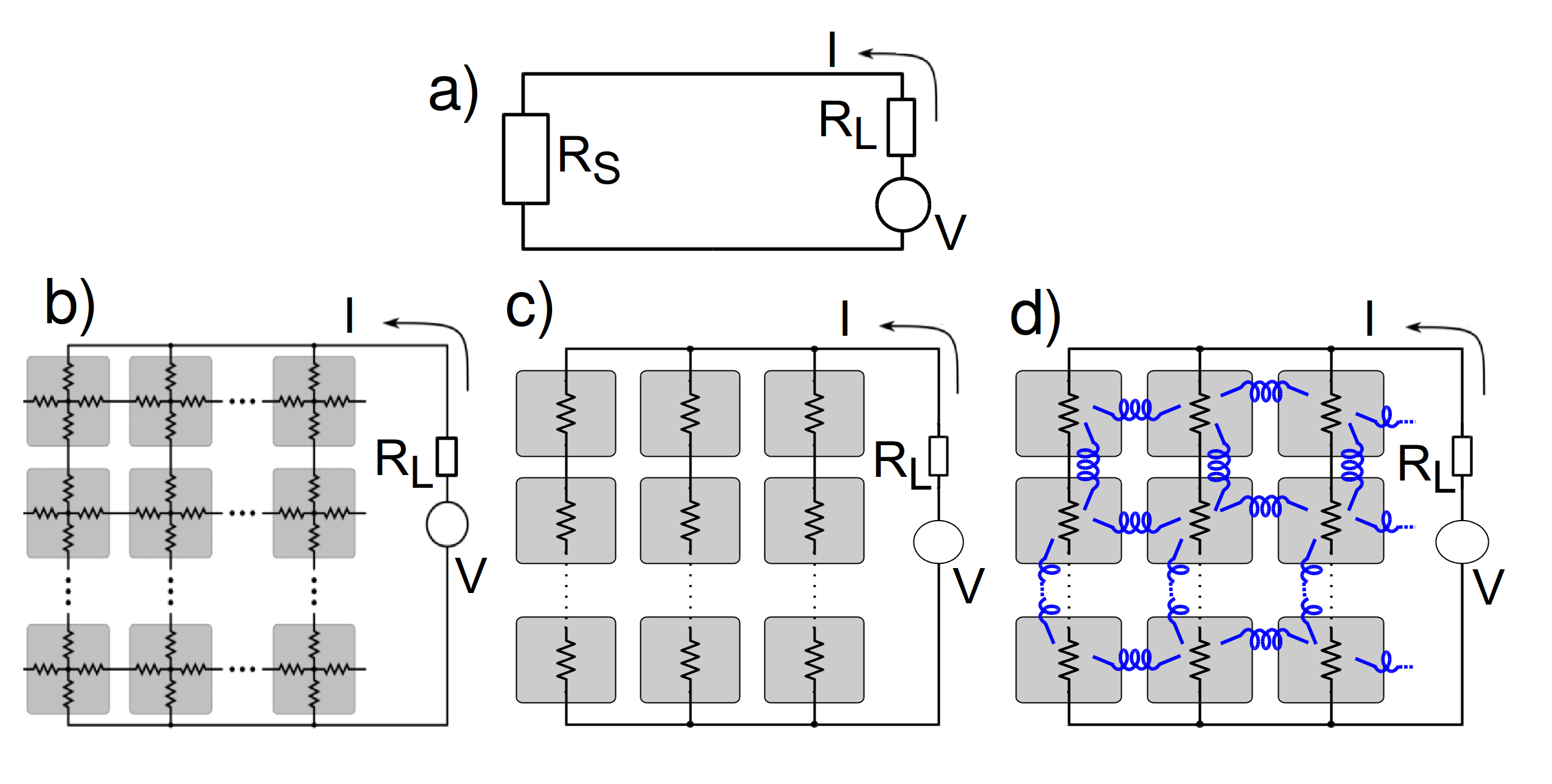
In the present numerical study we follow the methodology of Ref. Stoliar et al. (2013). In analogy to the actual experimental setup, we adopt an electric circuit with a constant load resistance , as shown in Fig.2.a. Thus, the resistance of the system and form a voltage divisor circuit. Denoting the externally applied voltage protocol, then the voltage on the resistor network is given by . The external voltage can be set as any arbitrary profile , which upon discretization of the time becomes at each time-step . Initially, all lattice cells are assumed in the MI state. Then, at every time step the full resistor network circuit is solved, obtaining all the local voltage drops at each cell site , and the total resistance between the top and bottom electrodes. For simplicity the electrodes are assumed perfectly metallic (see Fig.2.b) Stoliar et al. (2013).
At each time step, the state of the resistor network is updated following the procedure of Ref. Stoliar et al. (2013). The probability for a given insulator cell to undergo a local EMT, that is from MI to CM at time step is given by , where the constant is an attempt rate, is the charge of the electron, is the computed local voltage drop at the given cell, is the Boltzmann constant and the temperature. This is an Arrhenius like law, where the key feature is that the local electric field increases the probability for the cell undergoing a local EMT. This assumption should (hopefully) be fully supported by out of equilibrium many body calculations.
A crucial ingredient of the model is the metastability of the CM-state. In fact, if a given cell undergoes a MICM transition, then the metastable CM-state may relax back to the MI one. The transition rate for the relaxation is also given by an Arrhenius like expression , hence the model has a fixed relaxation time . We note that the in this relaxation process the field may be omitted since , so the voltage drop effect is neglected in the CM sites.
Thus, in the numerical simulation the 2D resistor network is solved at each time-step for a given protocol . The local voltage drops are computed for all cells . The state of the cells is updated according to the above probabilities. This gives a new value of the total (two point) resistance of the system, and then the simulation proceeds. We adopt . The unit of time in our simulations is the discretized time-step and the voltage is in arbitrary units.
The previous numerical studies Stoliar et al. (2013, 2014) showed that the resistive collapse in the EMT is due to the sudden formation of filamentary structures of CM phase, which connect the two electrodes. These structures grow, as expected, along the electric field lines. Less evident was the observation that while right after the percolation the filament connecting the two electrodes is quite inhomogeneous, it nevertheless continues to evolve till it rapidly reaches a rather homogeneous thickness Stoliar et al. (2013). This is illustrated in panel (a) of Fig.4. Since the numerical solution of the 2D resistor network is, by far, the most time consuming part of the numerical simulation, motivated by the previous observations, we explore a simplification of the simulation of the model that would dramatically boost the computational time.
This feature suggests that the transverse currents, i.e. perpendicular to the direction of the applied field, may not play a crucial role, at least after some irrelevant brief transient time. Therefore we numerically explored the possibility of neglecting the transverse currents altogether in our simulations. In Figs.4.b-d, we show a comparison of typical experimental data of the EMT for various applied external voltages and the respective result of the simulations for the 2D model (panel c) and for the case where the transverse currents were neglected (panel d). We see that the later simulations qualitatively capture the behavior, very similarly as in the 2D model Stoliar et al. (2013). In the present case, one should consider the thickness of the 1D filament (one cell) as a coarse grained version of the previous 2D one.
This simplification leads to a dramatic speedup of the simulations. In fact, instead of solving a 2D resistor matrix, we simply have a collection of 1D series resistor chains, which is trivially solved. This enabled us also to consider significantly larger systems and, more important, to simulate for longer times. This turns to be crucial for the systematic study of relaxation effects, which are relatively much longer than the typical time to dielectric breakdown. In addition, it makes possible a simpler analytical insight, which we will develop in the following sections.
This model has already provided valuable insights and very good qualitative agreement with experiments, such as the existence of a threshold field and the decrease of the delay time of the resistance collapse with the increase of the applied voltage Stoliar et al. (2013). However, as it stands, if fails to capture the existence of different relaxation regimes (ii) and (iii) as described in the Introduction. In fact, the model has a single intrinsic relaxation time, which is solely set by the energy difference between the electronic energy barrier and the metastable CM-state, .
Thus, in order to qualitatively capture the observed experimental behavior where strong voltage pulsing may realize low resistance states that are long-lived, we shall extend the model by making an additional assumption. Specifically, we shall introduce the energy cost associated to the formation of a MI-CM boundary interface. We may rationalize this as an elastic energy that originates from the structural strain created at the boundary between the two distinct electronic phases. In fact, experimentally, using STM techniques, it has been observed a giant electro-mechanical effect that was interpreted as a strong self-compression of the lattice structure in the metal state Dubost et al. (2013). Therefore, we add to the model the assumption of an elastic deformation energy , which is a supplementary energy cost associated to the transition when two nearest neighbor cells would end in different states. In other words, it is an energy penalty for creating spatial inhomogeneities. As we shall see, this assumption creates spatial correlations in the way that multiple filaments grow. In our previous model, filaments would grow at random, essentially uncorrelated positions, across the system. However, the addition of the elastic energy promotes the grow of new filaments neighboring a previous one. Thus promoting the thickening of filamentary structures.
The simplest way to include this in the model is by adding this effect into the definition of the energy barrier.
Thus, we may write the energy of the barrier of the site of the lattice as
| (1) |
with the elastic energy cost being,
| (2) |
where the variable indicates the current state of the cell (say, MI and CM ), is the proposed new state for the cell (i.e. ), the index of the sum runs over the number of nearest neighbors , and is an elastic constant.
Thus, if initially the cell is in the same state as all of its neighbors, then the barrier to overcome is (maximally) increased from the electronic value by the amount of corresponding to the maximal mismatch. If, on the contrary, the cell is initially in a different state with respect to all of its neighbors, the barrier to overcome is solely the electronic one, as since all cells would end up in the same phase. For simplicity, we shall consider here that the range of the elastic term is only to the nearest neighbors, so in the present 2D lattice . There is of course freedom to choose longer range interactions. We shall come back to this point later on.
As we shall see, the low-resistance states may become long-lived as the filamentary structures grow thick. Thus, for the sake of clarity in the presentation of our results, we shall first dedicate the next section to describe the formation of CM filamentary structures and how their thickness may grow under strong applied voltages. Then, in the following section we shall describe how the relaxation time may be significantly affected by the inclusion of the elastic deformation term and how it may qualitatively account for the various EMT regimes discussed before. We finally also compare our model behavior and experiments involving the application of trains of short voltage pulses, which bring us qualitatively closer to the realm of spiking neurons.
.3 Filament Formation and Growth
The EMT proceeds through two distinct stages: the first is the creation of low resistance filamentary structures that inter-connect the electrodes; the second is the successive reabsorption of the filaments as the system recovers the high resistance state. The first one occurs under the application of a strong external voltage, while the second takes place when the applied voltage is switched off. The present section is devoted to describing the first process.
The formation of the filaments under the application of an external voltage in the present model was already qualitative described in Ref.Stoliar et al. (2013). The main features were the existence of a threshold field for the formation of filaments and that the number of filaments (or the fraction of phase change in the system) grows with the magnitude of the applied field via a process of subsequent multiple filaments formation. The inclusion of the elastic term does not change the main basic mechanism, however, there are a few qualitative differences that we shall explore in this section.
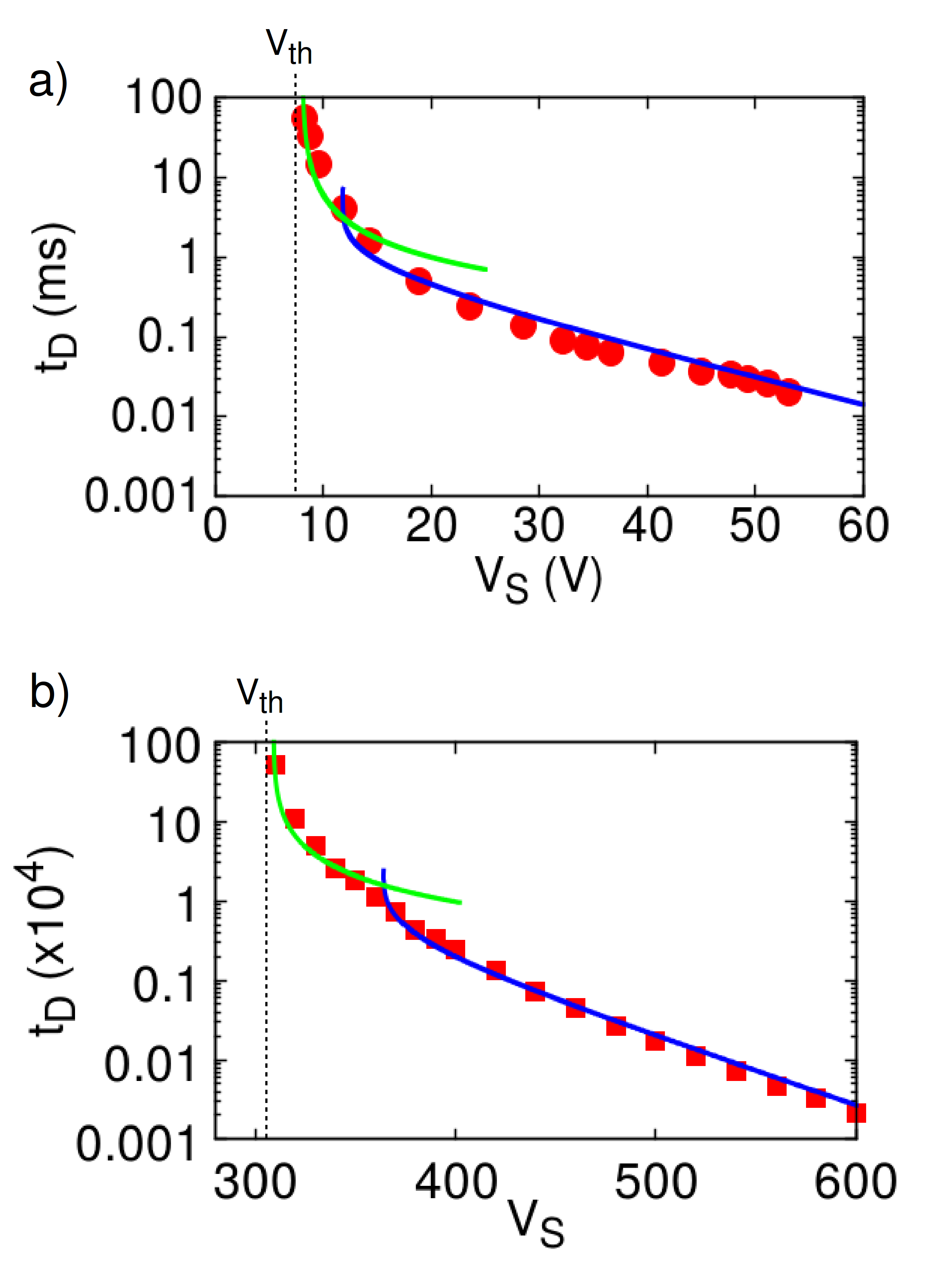
In Fig. 6 we show the dependence of the delay time for filament formation with the applied voltage on the system (), both for experimental data in a GaMo4S8 and for numerical simulations. We observe that the model behaves qualitatively similar as the experimental system, with a variation of spanning many orders of magnitude. Both data sets show a linear behavior in a semi-log plot for short times and large , and a clear slowing down of the dynamics as approaches the . At the threshold voltage the delay time should diverges, however it is difficult to access that regime both, experimentally and numerically.
We shall now consider in detail the formation of the filament from a dynamical point of view. This will allow us to derive approximate expressions for the delay time .
The formation of filaments is a sudden event, thus the state of the system previous to the EMT breakdown still has the vast majority of cells in the initial MI state. Thus the system before the rupture is quite homogeneously MI. This implies that the role of the elastic term before the rupture is essentially to renormalize the value of the electronic barrier height to for the MI sites, which upon transition to the CM state find themselves surrounded by neighboring MI site. In contrast, any site that has already become CM, under relaxation to the MI does not see any elastic barrier, since all his neighbors are MI. Then this allow us to understand that the elastic term just produces slight changes in the value of the threshold voltage and the time Stoliar et al. (2013).
One may gain analytic insight in the process of the initial filament formation and threshold behavior by considering the dynamical behavior given by the deterministic partial differential equation that follows from the probability rates of our model in a continuum limit. The production rate of CM-cells is given by the difference between a gain and a loss (leaky) term with their respective probabilities.
| (3) |
where and are the time dependent number of cells in the CM and MI state, respectively. is the number of cells between the top and bottom electrodes, i.e. the linear longitudinal dimension of the system. The elastic energy term in the model depend on the specific local configuration, so for the present analysis we have approximated them by the parameters and , which would correspond to average elastic energies of a CM and a MI cell, respectively. The voltage is the voltage drop on the MI cells, . Since , the total applied voltage essentially falls on the high resistivity cells MI, with . Hence, the gain transition rate increases exponentially with increasing .
The reader that is not interested in the details of the dynamical analysis of the rate equation that provides approximation for the delay time (shown in Fig. 6) may skip to the end of Eq. 8.
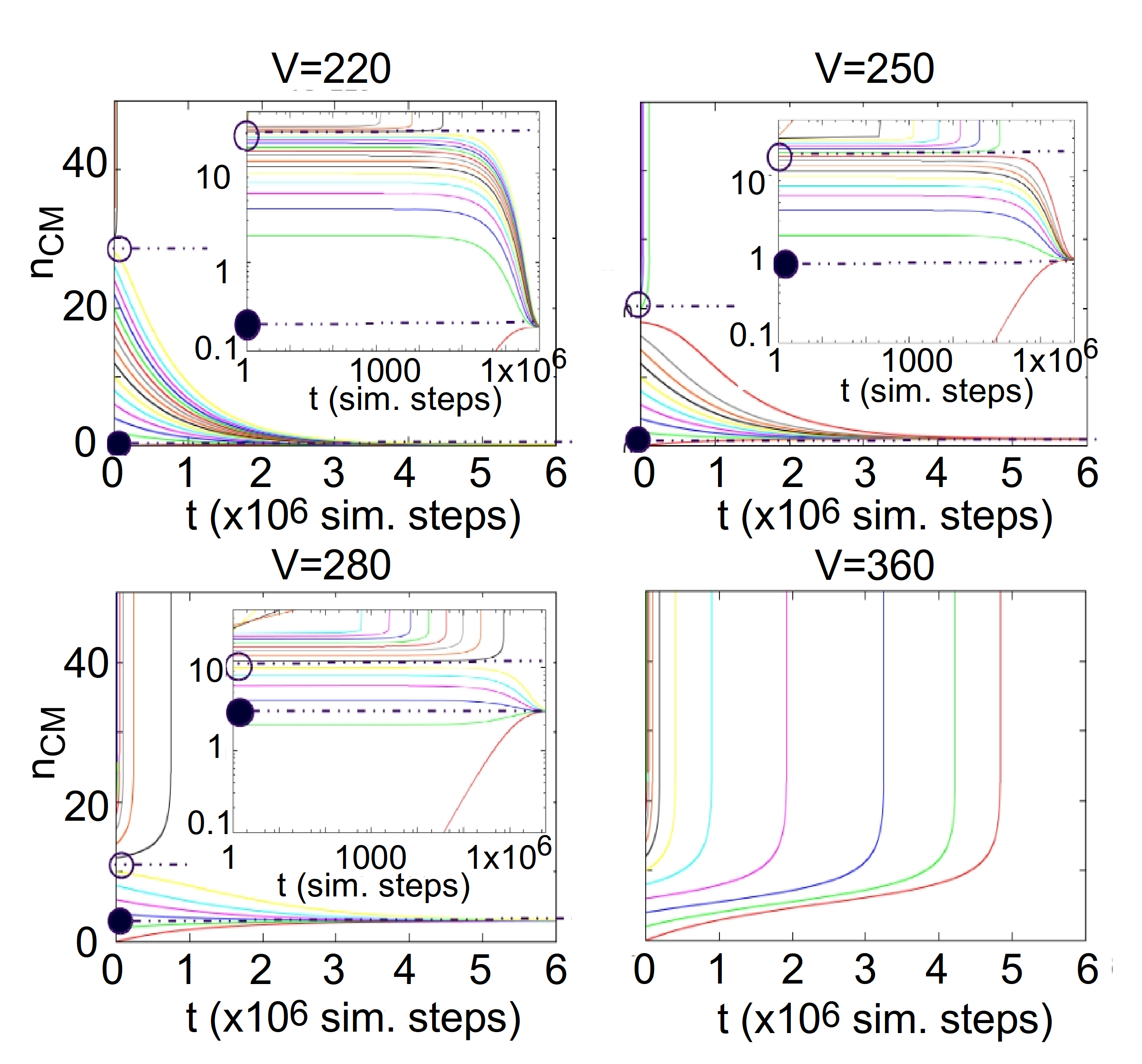
The rate equation has a stationary solution when . It is given by the balance between the gain and the loss term. We shall consider the existence of such a solution as a function of the external voltage . A geometric solution of the problem is shown in Fig.5 where we plot the gain and loss terms as a function of the variable at increasing values of and all other parameter left fixed. The way to interpret this plot is as follows: at any given value of either the gain (red) or the loss (blue) rate is bigger. If the gain is bigger, then will evolve to the right, that is, to higher values. If the loss is bigger, it evolves to the left. The equilibrium of is where the gain and loss transition rates are equal. We observe in the two top panels of the figure that there are two points where the gain and loss terms cross. However, it is not difficult to see that only the lowest one (black dot) corresponds to a stationary stable equilibrium state, while the higher one (empty dot) is an unstable equilibrium point. Varying the parameter , there is a critical value where the two crossing points “collide” at . The interpretation of this critical is the finite threshold value . For higher values of , as shown in the last panel, there is no stationary state for , which means that the gain rate is never compensated by the loss rate and there is a runaway evolution of (indicated by the arrows). This Instability signals the formation of the first filament.
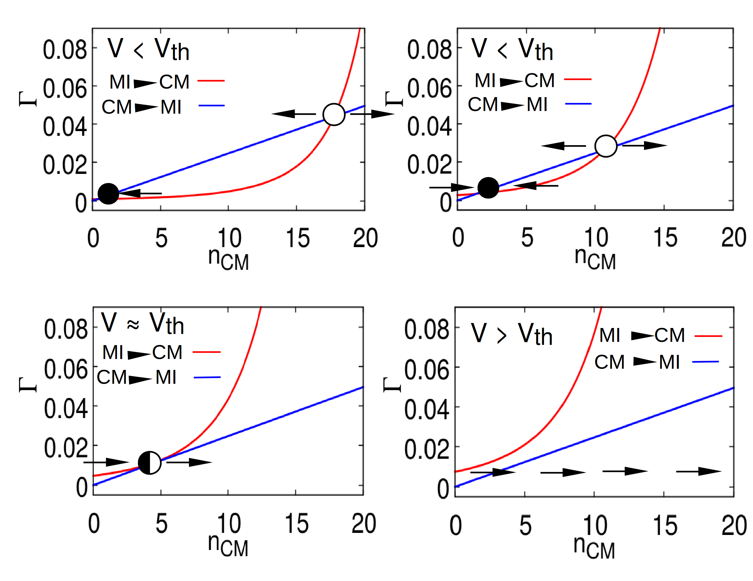
This process is not an uncommon situation found in dynamical analysis and is termed a saddle-node bifurcation Strogatz (2000). For further details, an analysis of the numerical integration of the rate equation is shown in the Supplementary Material. We shall now derive two approximate expressions for the delay time . One is simpler and valid at shorter times and higher applied and the other is for longer times and closer to .
If the parameters of the model are such that , then one may approximate the rate equation LABEL:ncm by
| (4) |
If then an avalanche event will occur, as described above. Before the avalanche can take place there is a period where the evolution of the system (i.e. of ) is dominated by the slow dynamics at the proximities of the former stationary point where . It is the region where the gain and lose rate curves are approximate parallel (red and blue curves in Fig. 5). Once the evolution of overcomes this regime, it rapidly increases to , i.e. the filament forms with an avalanche. Thus, we may neglect the duration of the sudden event for the estimation of the delay time for the filamentary formation and obtain an approximate expression by integration of Eq. 4 from 0 to ,
| (5) |
where is the first term in the right hand side of Eq.4, is the exponential factor in the second term of the same equation and was assumed a constant.
We used the expression above to produce fits of the experimental and numerical data at short times. This is shown in blue curves in Fig. 6, where we observe that the approximate expression can reproduce the variation in of more than two orders of magnitude. The fitting parameters are summarized in the Table 1.
At lower , and as we get closer to the threshold, the approximation made before is expected to fail, as mentioned before. To describe the region close to the threshold we need to more accurately describe Eq.LABEL:ncm expanding around the bifurcation point (,). Thus, defining , and using that at the bifurcation point and , we get to the lowest order
| (6) |
where
| (7) |
where the derivatives are evaluated at (,). Integrating, we obtain for
| (8) |
The fit according to Eq.8 is shown in solid green lines in Fig.6 for both, experimental and numerical data. We observe that the approximation captures the behavior of near the thresholds. The fitting parameters are summarized in the Table 1.
We now turn to describe one of the new features introduced by the elastic term in our model, namely the thickening of the filament with time. The width of initial filament is is just one cell. Thus, after it forms the resistance of the system drops from a high value to a lower value //] , where is the width of the resistor network and is the length (i.e. distance between electrodes) as before. The decrease of provokes a reduction of the voltage applied on the network according to , where is the load resistance. Hence, the new value of may be larger or smaller than . In the former case the system will undergo a second filamentary formation, again according to Eq.5 but for a new (lower) value of . After the formation of the second filament, will drop further, and the process of filament formation will continue until . This feature was already present in the previous model without elastic term. Thus, in that case, the position where the filaments form was essentially random and did not have any spatial correlation.
| Experiments | Simulations | |||
|---|---|---|---|---|
| Region | High Voltage Region | Region | High Voltage Region | |
| 110 | 100 | 70 | 70 | |
| 15 | 15 | 31.85 | 31.85 | |
| 0 | 0 | 0 | 0 | |
| 10 | 10 | 49.7 | 47.8 | |
| 0 | 0 | 12.7 | 12.7 | |
| 0.08 | 0.05 | 0.07 | 0.04 | |
| 2000 | 2000 | 50 | 50 | |
| 74K | 74 | 74 | 74 | |
| 8.0 | - | 1.97 | - | |
| 1 | 1 | |||
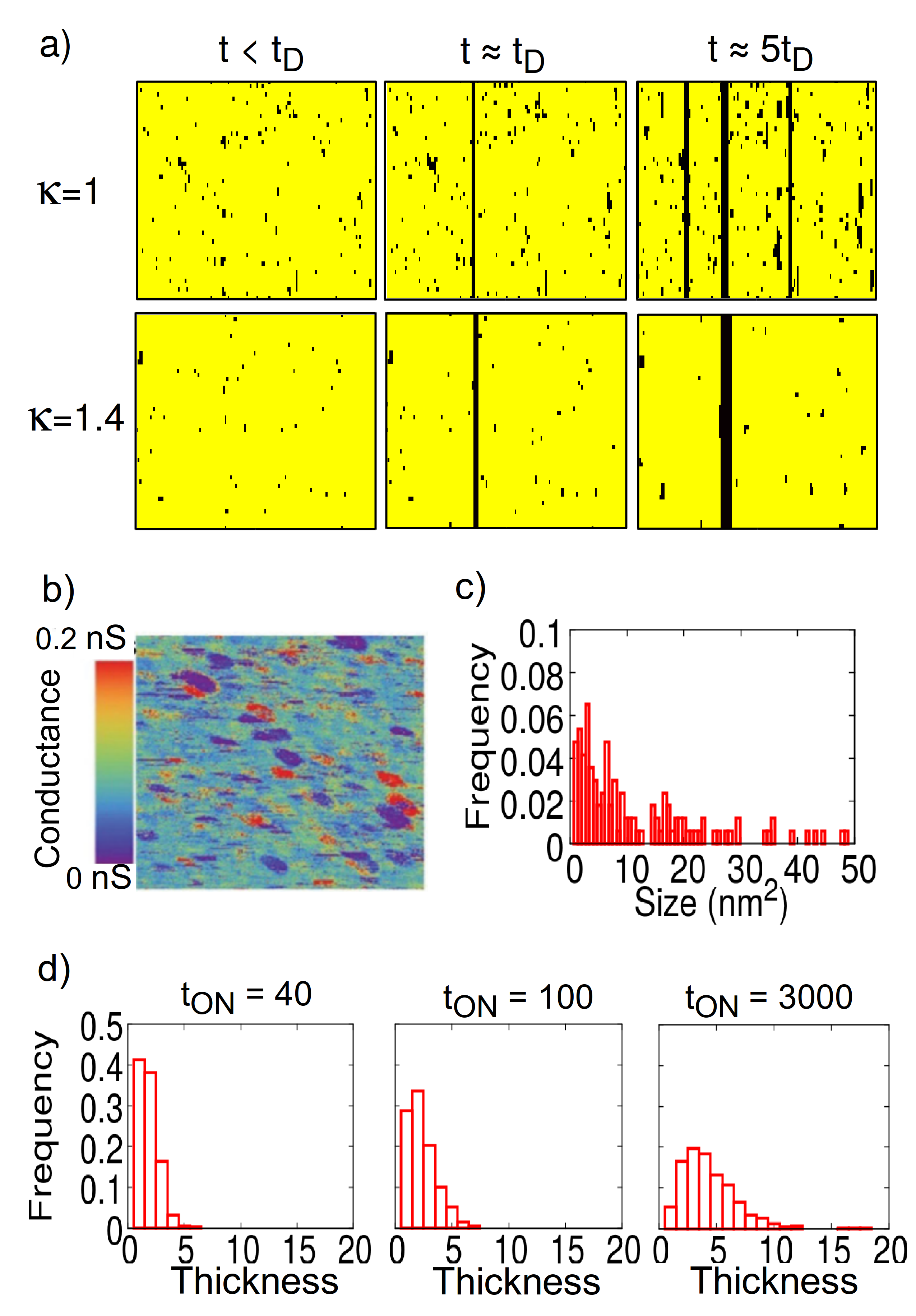
In contrast, in the present model the elastic energy term favors the growth of adjacent filaments, or, in other words, it favors the thickening of the filaments. This is easy to see, since an isolated filament requires the phase change of cells into the CM-state, while being surrounded by the other MI phase. That implies a maximal local elastic cost (see above). However, if a filament is already in place, the phase change of a cell adjacent to it is less penalized, hence has a higher probability to occur. This feature is seen in the panels of Fig.7.a, where we show snapshots of the system before the formation of the first filament (), just after its formation () and at a later stage (). We see that both process have occurred, more filaments are present but also the filaments grew thicker. Evidently, the higher the value of the elastic constant and/or the longer the range of the elastic interaction, i.e. , the more favorable would be for the thickening process with respect to new individual filament formation. Results for two different are shown. In addition, the increase of may enhance the formation of CM-clusters before the generation of filaments, which, in turns, may affect the value of . As seen in Fig.6, this last effect plays little role for .
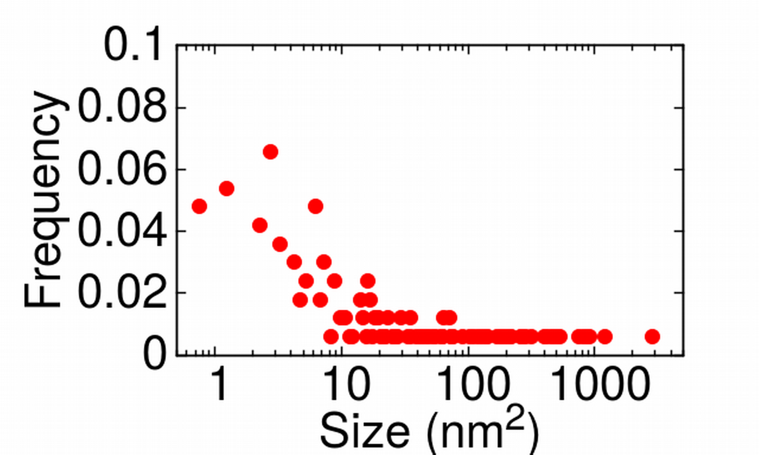
This feature may allow us to interpret the experimental results reported by scanning tunneling microscopy (STM ) on a cleaved surface of a GaTa4Se8 compound Janod et al. (2015) after the EMT. The image data in Fig.7.b show the variations in the conductance map due, presumably to the cross sections of the conductive filamentary structures that were created by the EMT (in red). The distribution of areas of these conductive cross sections, which we associate to the filament thickness in our model, are quantified in the histogram in Fig.7.c. We can compare these data to our model simulation results. In the three panels of Fig.7.d we show the evolution of the histogram of filamentary thickness distribution during the application of a continued pulse voltage. We observe that, consistent with our previous discussion, the histogram distribution slowly drifts to higher thickness and is in qualitative agreement with the experimental data. We notice here that when typical thicknesses are greater than about ( being the width of the sample) the nucleation of separated filaments has shown to be a relevant effect (i.e. the creation of big filaments via the percolation of smaller ones). In the STM image we observe cross sections with areas up to about (being x the total area), suggesting that is effect is not relevant for the experiments analyzed in this work 111For a better comparison with simulations, in the histogram of Fig.7.c we consider cross sections up to a few tens of . The full distribution is shown in Supp. Mat.. Thus, we will restrain our study to filaments thicknesses below .
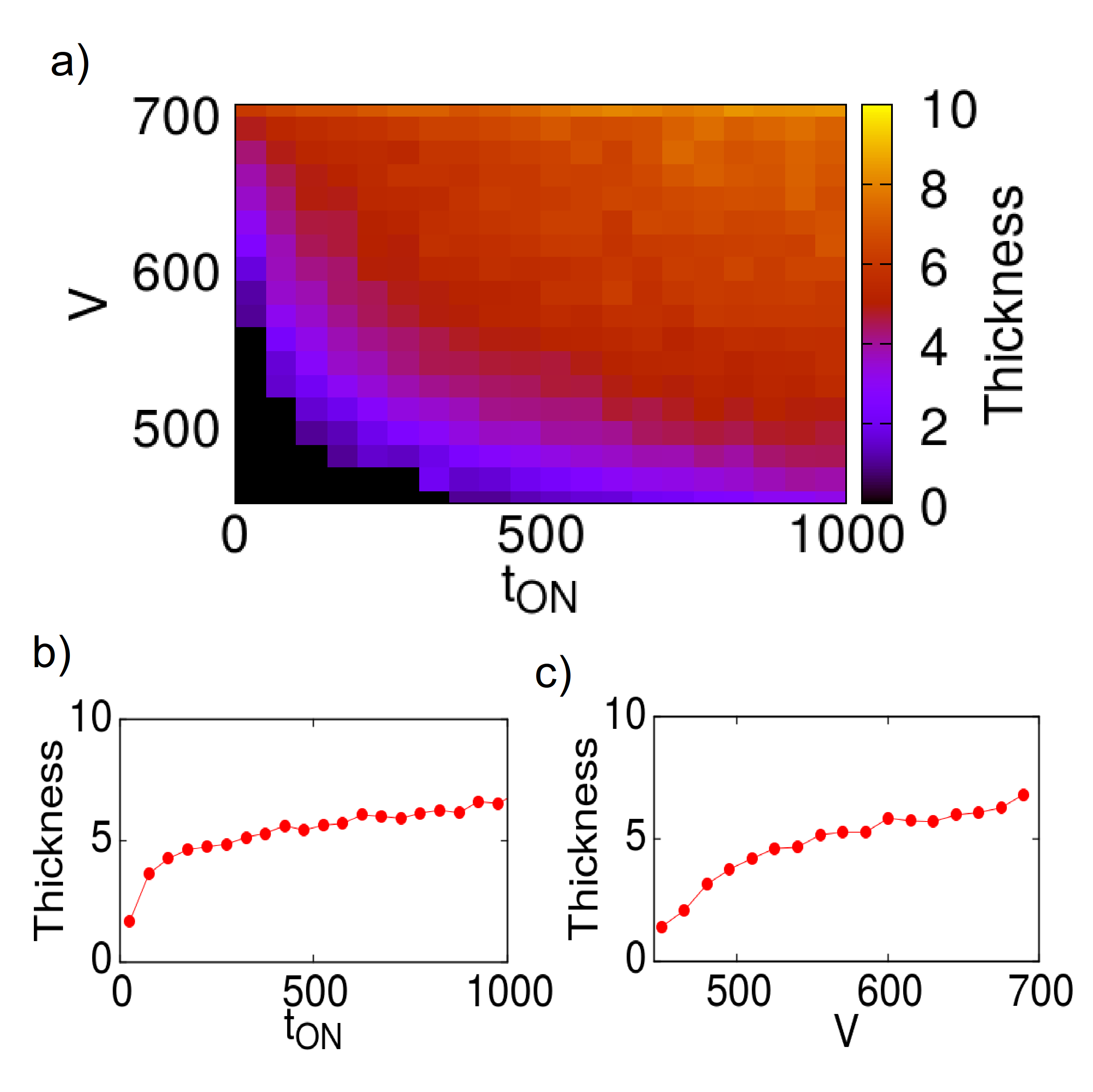
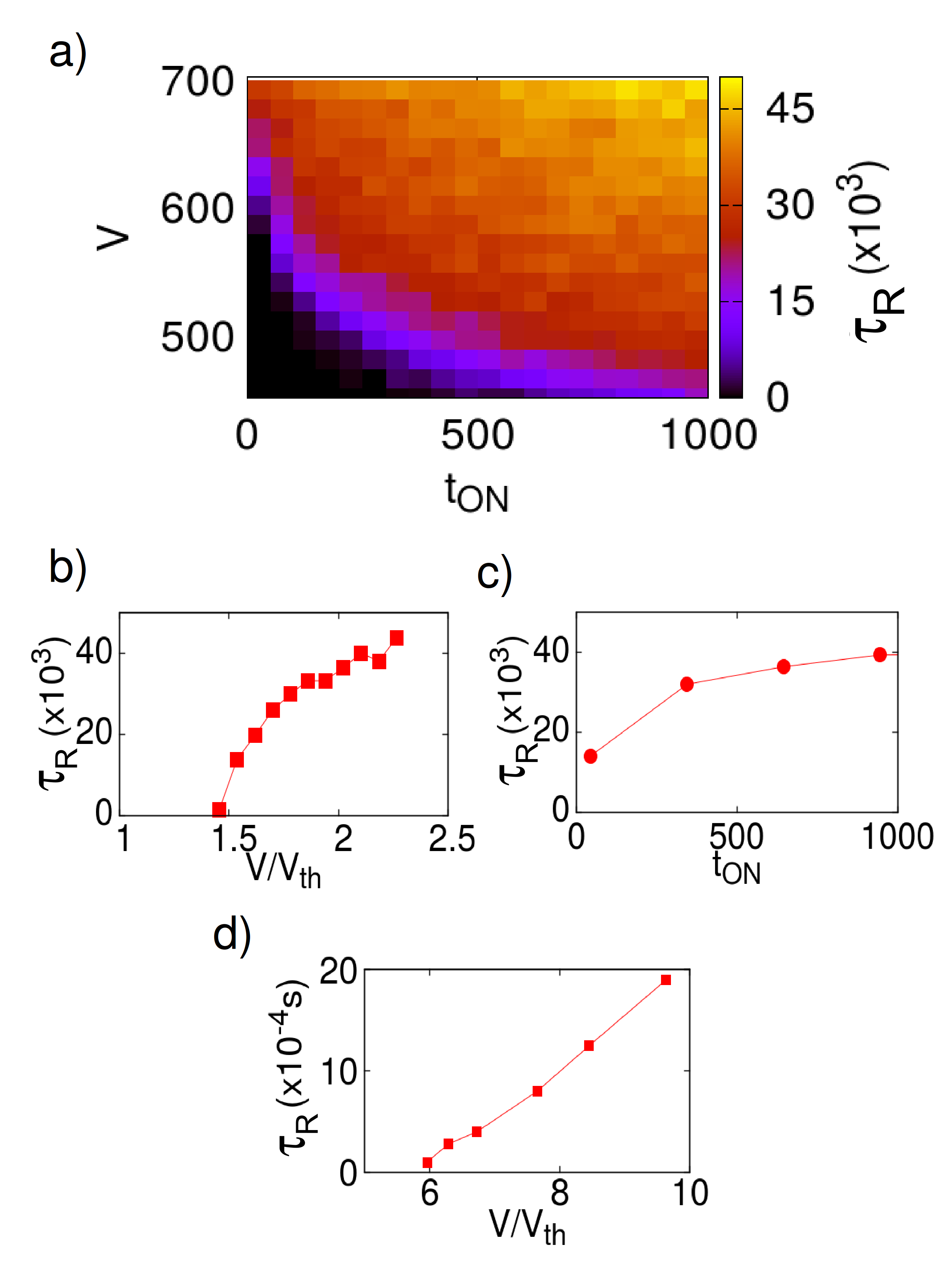
The systematic thickness grow of filaments in our model is further characterized in Fig.8. We show a color map (panel a) of the largest thickness of the formed filament as a function of the duration of the applied pulse voltage () and its magnitude (). The two panels b and c respectively show cuts of the color map at fixed and fixed The results are obtained as the mean over 100 realizations. The parameters used for the simulations are the same as in Fig.4.
.4 Filament reabsorption: retentivity in the recovery phase
We now turn to a central part of this study, which is the relaxation of the low resistance state back into the Mott insulator state after the applied voltage pulse is terminated. The proper description of this process is crucial for the understanding of the recovery phase in neuromorphic applications of the EMT for neuron analogue electronic devices Stoliar et al. (2017).
The previous modeling of the EMT, which did not include the elastic term, predicted that the conductive low resistance state always returns back to the high resistance state with an essential constant relaxation-time rate. The cells in the CM metastable state relax back to the MI with a single characteristic time and they do that randomly. So the filaments disintegrate randomly as well. We shall now study how the addition of the electro-elastic effect in the model modifies this feature.
In a low resistance state there are filamentary structures which are composed of a relatively high number of cells that switched into the metastable CM-state. These structures are induced by an external applied voltage. After the voltage application is terminated, the CM cells start to relax back to the high resistivity MI-state. The relaxation time for the total number of cells to return to the MI-state is long. However, this is not the physically relevant time for the experiments. In fact, the experimental observation of the relaxation of the system is through the behavior of the recovery of the resistance . So the important quantity to monitor in our model is when the filamentary structure of CM-cells breaks up or loses the percolation.
In our previous model, the cells forming the filament relaxed in a random fashion. In contrast, in the present case where we added the electro-elastic term in our model, we shall see that the filaments relax differently. Rather inversely to the case of filamentary growth by thickening, the dissolution of filaments occurs by thinning. In fact, as we shall see, the cells on the border of the filament have higher probability to relax to the MI-state compared to those in the interior of the filament.
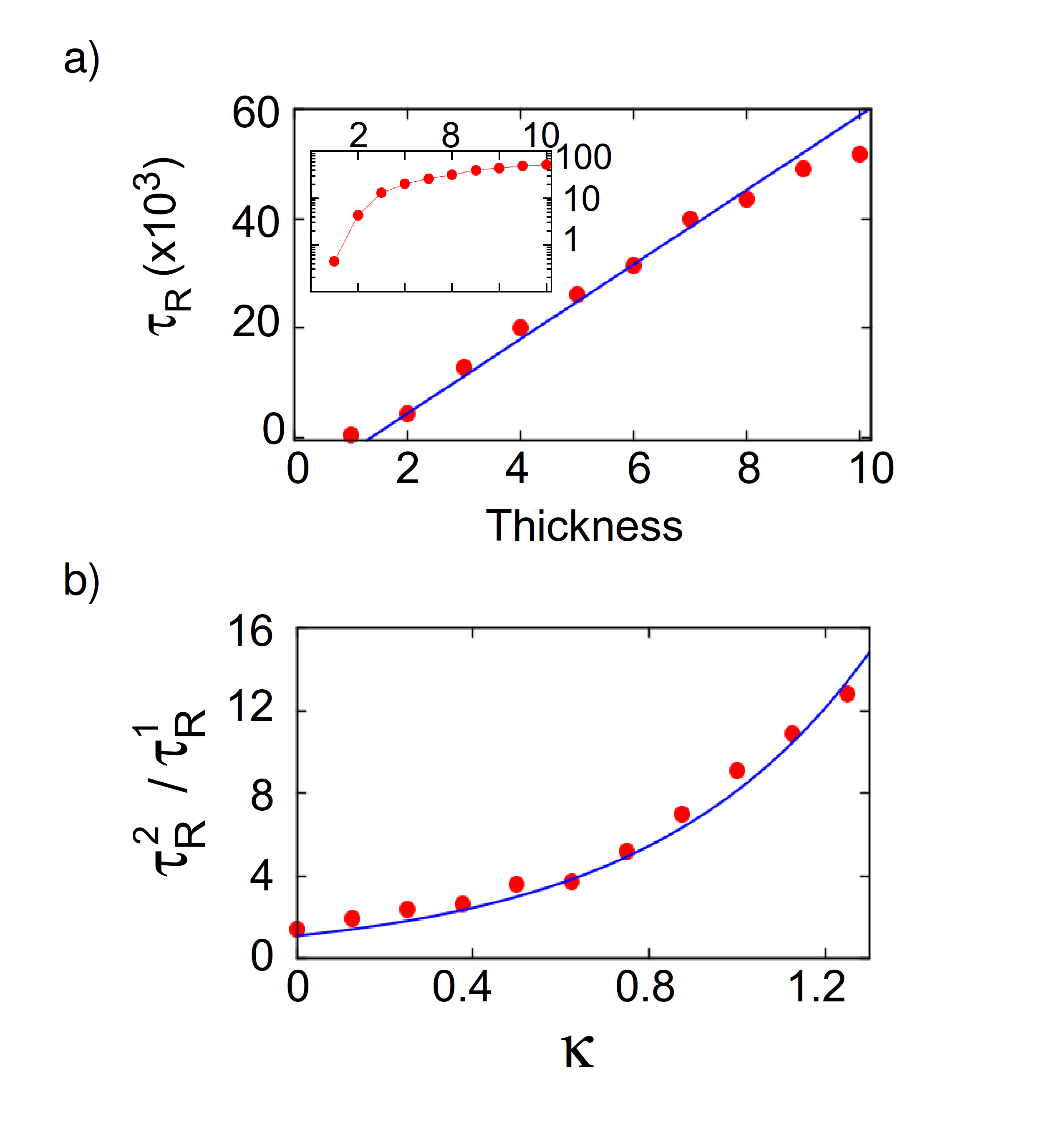
In order to perform a systematic study of this process, we shall start from “artificially” well defined initial states consisting of homogeneous filaments of cells in the CM-state that we let relax back to the insulator. We shall consider initial filaments of different thickness and then record the time it takes for them to break up. Since in our model this process is subject to statistical fluctuations we average our results over a large number of realizations (typically 100). We shall denote this time as it indicates the time that a filament keeps its high conductive state till it relax to the insulator one. This quantity may also be denoted retentivity.
In Fig.9 (left panel) we show results of our simulation studies for the dependence of with the initial filament thickness , between and . We observe that there are three different regimes. An initial exponential increase, which then becomes linear and finally saturates for higher values of . Overall, increased by two orders of magnitude for filament thickness of just a few units. The fast initial increase, of a full order of magnitude when comparing to , follows from the presence of the elastic term. This renders much less probable the relaxation of cells in any one of the two adjacent filaments with respect to a single one. In the former case, any cell of a filament is surrounded by other cells of the same type, while in the later only by (out of ). This effect enters into an exponential in the probability (see Model section above). As one may distinguish between central filaments or border filament. Cells belonging to central filaments have all their neighbors in the same state. Hence the eventual elastic mismatch maximally penalize the relaxation. In contrast, cells in the external boundary of the filament only have neighbors in the same sate. Hence boundary cells will relax faster. An internal cell would only get a good probability to relax by becoming part of the boundary, i.e. after outermost neighboring cells relax. This feature leads to a continuous “thinning” effect of the filaments, and it progresses at an approximate constant rate, which results in the observed linear dependence with . At higher values of a saturation effect becomes evident, as the thinning time starts to compete with the probability for relaxation of internal filament cells (i.e. with those inside an homogeneous CM phase).
We may easily estimate the relaxation time of a unitary filament from the loss term of the dynamical evolution of the cells of expression (LABEL:ncm),
| (9) |
being the elastic part of the energy barrier of the -cell in the filament, which is assumed constant for all the cells in the same unitary filament. The rupture condition for a unitary filament is given by the relaxation of a single cell (since we neglect transverse currents), i.e. . A conductive individual filament has initially . Therefore,
| (10) |
and we simply get:
| (11) |
where denotes the time for rupture of a unitary filament. From our previous qualitative discussion we get that for cells in an isolated filament of . Then for cells in the outer boundary of filaments of , and for cell in the interior of a thick filament (). The exponential dependence is explicit in Eq.11.
Then, recalling from our discussion that the filaments relax by progressive thinning, we may simply estimate the total time for the full rupture of a filament of thickness as,
| (12) |
where refers here to unitary border filaments. From the above equations we may focus on the simple case with and , which produce the largest relative retentivity gain. The ratio for the respective gives
| (13) |
which corresponds to the blue solid line fit of Fig.9.b. Here correspond to the number of neighbours in the CM state for each thickness . This expression highlights the exponential dependence on the elastic constant parameter . Evidently, in systems where the field induced dielectric breakdown is due to a structural change, one may consider that is very large and the change cannot be undone except by means of inducing a new structural change. We may then consider that becomes effectively divergent. Interestingly, this is the situation in non-volatile resistive switching oxides, such as TiO2, HfO2, NiO, CuO, etc, that form filamentary structures which involve ionic migration. One may also contemplate the possibility that in the Mott systems that presently concern us the regime (iii) where the resistive change may be non-volatile (or very long lived) may also involve a volume change of nano-domain size regions of the crystal. Then, the non-volatility may be due to pinning by strain defects induced by the strong electric field Janod et al. (2015).
On the other hand, it is intuitive that the retentivity time may be significantly augmented by increasing the range of the elastic term. One may consider, for instance, next nearest neighbors or any longer finite range. Indeed, elastic strain involves several lattice units in real materials Wilkinson et al. (2006) . At the level of our model, we find this effect is so severe that, even upon increasing the range of the elastic term to the next nearest neighbors, our simulations become prohibitively slow. The mathematical analysis of the behavior and dependence of model parameters can be carried on along similar lines as we did above (see Sup. Mat.). Thus the origin of the long (and possibly infinite) retention times in regime (iii) may be due to long range strain induced by the filamentary growth.
.5 Resistance relaxation with an applied voltage bias
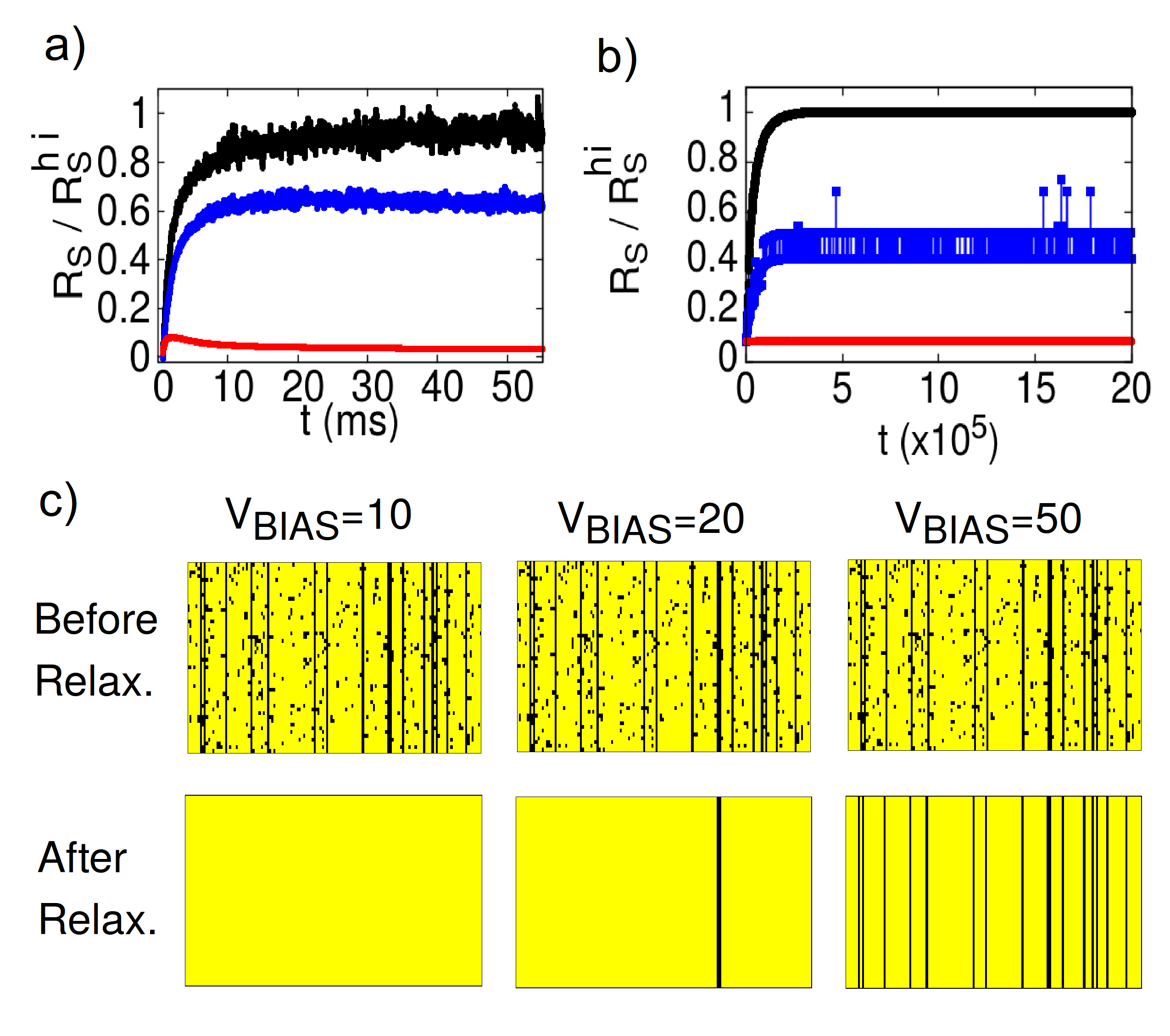
We shall now discuss an interesting effect due to the introduction of the elastic energy barrier term in our model related to the electric stabilization of filaments. In other words, electrically prevent the filament break-up and reabsorption. In previous sections we have seen that a minimum threshold voltage is necessary for filament formation. In this section we consider a different issue, namely, what is the minimal low-voltage that needs to be applied to sustain an already fully formed filament. The interest of this question is that it may be experimentally tested as further validation of the present model.
In Fig.10 we show our simulation results for a resistive switching protocol where a small bias voltage () remains applied during the relaxation process. Along with our numerical results we also show in the figure actual experimental data obtained in GaMo4S8 sample under a qualitatively similar voltage protocol. Specifically, the experiment was performed as follows: i) at a bias voltage is turned on, ii) at a high voltage pulse is applied for a time , iii) at the applied voltage returns to and the evolution of the resistance of the system is observed. The bias voltage remains applied during the entire process. The times and and the total applied voltage during the pulse are kept constant so that the switching voltage is the same in all realizations. In the figure we show the results of this protocol for three different . We observe that both, in experiments and simulations, the asymptotic relaxation value of the resistance depends on the applied . In fact, at the highest applied bias (red curve), we see that the resistance does not recover to the initial state but remains at a lower value. To get a better understanding of this behavior we show in Fig.10.c snapshots of the simulated resistive network for each at two different times: a short one, right after the pulse is terminated at and a longer when the asymptotic resistance state is reached 222As a technical side note we notice that we kept the same “seed” for the pseudo-random number generator in all three simulations for the sake of a more meaningful comparison.. We observe from the short-time snapshots (upper panels) that the resistive change is rather independent of the applied (sub-threshold) bias-level, as a very similar multi-filament structures are realized in all three cases On the other hand, for the asymptotic state the system shows qualitatively different states. In the lowest bias case, the whole filamentary structure is reabsorbed. In the intermediate bias case only a single filament persists, which was the thickest. While in the higher bias case, all filaments formed during the pulse remain at asymptotic times. We also note that all isolated metallic regions (clusters) do relax to the insulator state in all three cases.The fluctuations observed for the intermediate voltage in panel (b) (blue curve) are due to rapid rupture and reconnection of small sections of a filament (i.e. a transitory decay to the insulating state). This effect may actually happen in real materials, however in our simulations it is likely overemphasized due to the finite size.
.6 Complete pulse-voltage protocol
In this final section we shall consider the full-time behavior of the system, that is the whole process of formation and subsequent reabsorption of filaments. We shall adopt two different applied voltage protocols: a single pulse and a train of pulses. The former case is simplest to analyze as is closely related to the discussions of previous sections. In contrast, the interest of applying train of pulses Stoliar et al. (2017) is that it bring us closer to the situation of actual neurons, which are excited by electric spikes.
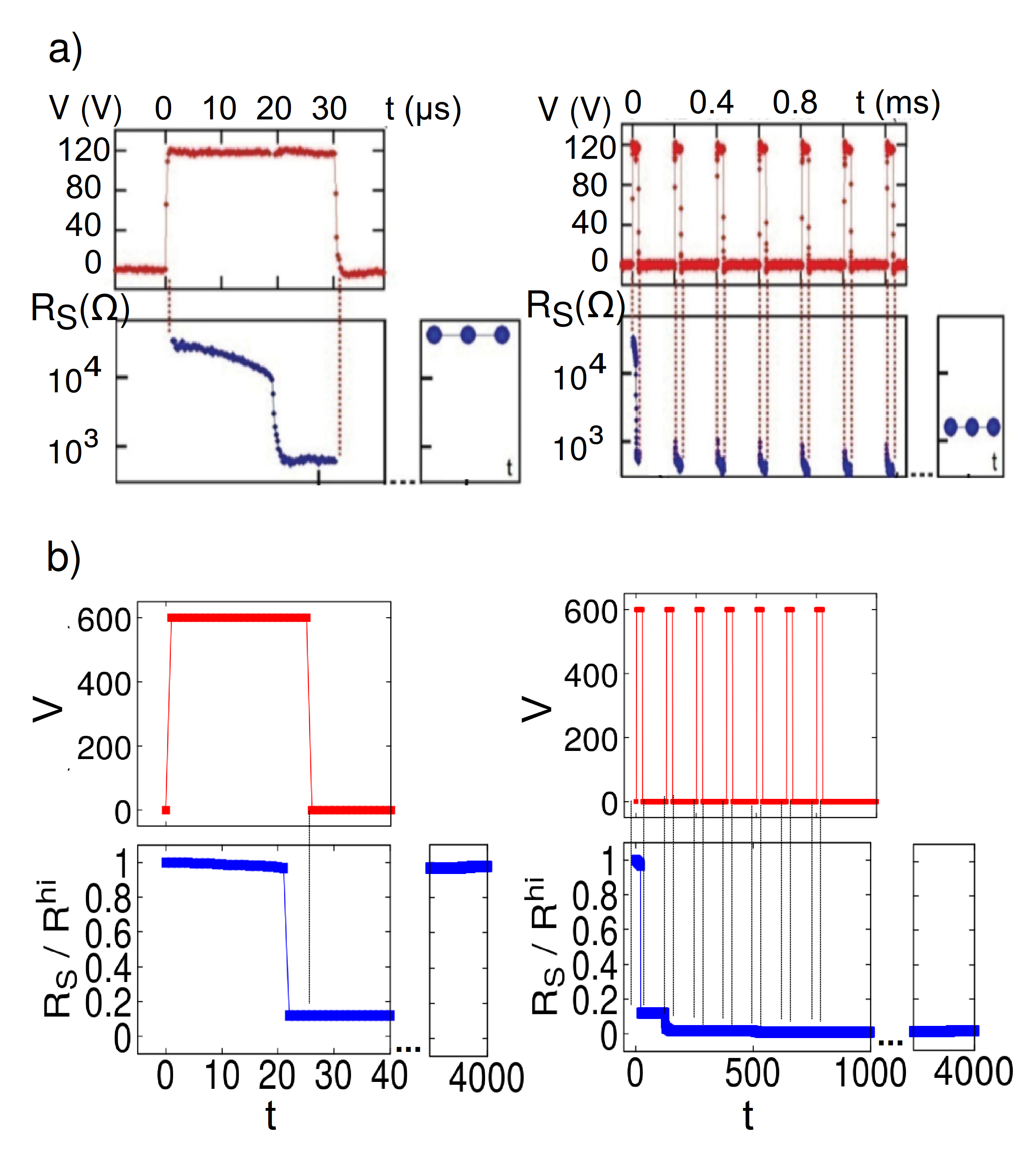
In Fig.11 we show the full time evolution of the resistance during the application of a single pulse for both simulations and experiments on a GaMo4S8 sample (same sample as in Fig.6) . A single voltage is applied for a fixed duration , then is set to zero. We show data for two different applied voltages. We observe the significant dependence of the retention time with the applied voltage. We see that a relatively small change in the strength of the applied pulse produces a great change of the retention time. For example, in experiments a change in the voltage from to produces a change in the retention time of a full order of magnitude (from approximately x to approximately x). Similarly in the simulations, a change in the voltage from to , produces a change of the retention time by a factor of (from approximately x to approximately ).
These results permit to rationalize the existence of the regimes (ii) and (iii) that we described in the introductory section before. In Fig.12 we show our simulation results for the retention time as a function of parameters of a single voltage pulse: intensity and duration time . In the color plot of panel (a) we observe that the retention of the filaments may be increased by either incrementing or . The key point being that any one of these two parameters contribute to thicken the filaments. The dependence of the threshold with the duration of the applied pulse can also be clearly observed. This is basically the effect of the delay time that was discussed in previous sections: At a given applied voltage there is a delay time for the transition, which implies that the pulse duration must be above the delay time to actually produce the filament formation. The two panels (b) and (c) show two cuts of the color map for fixed and respectively. All these results correspond to the mean over realizations. Finally in panel (d) we show the evolution of on a GaMo4S8 sample as a function of the applied voltage for fixed .
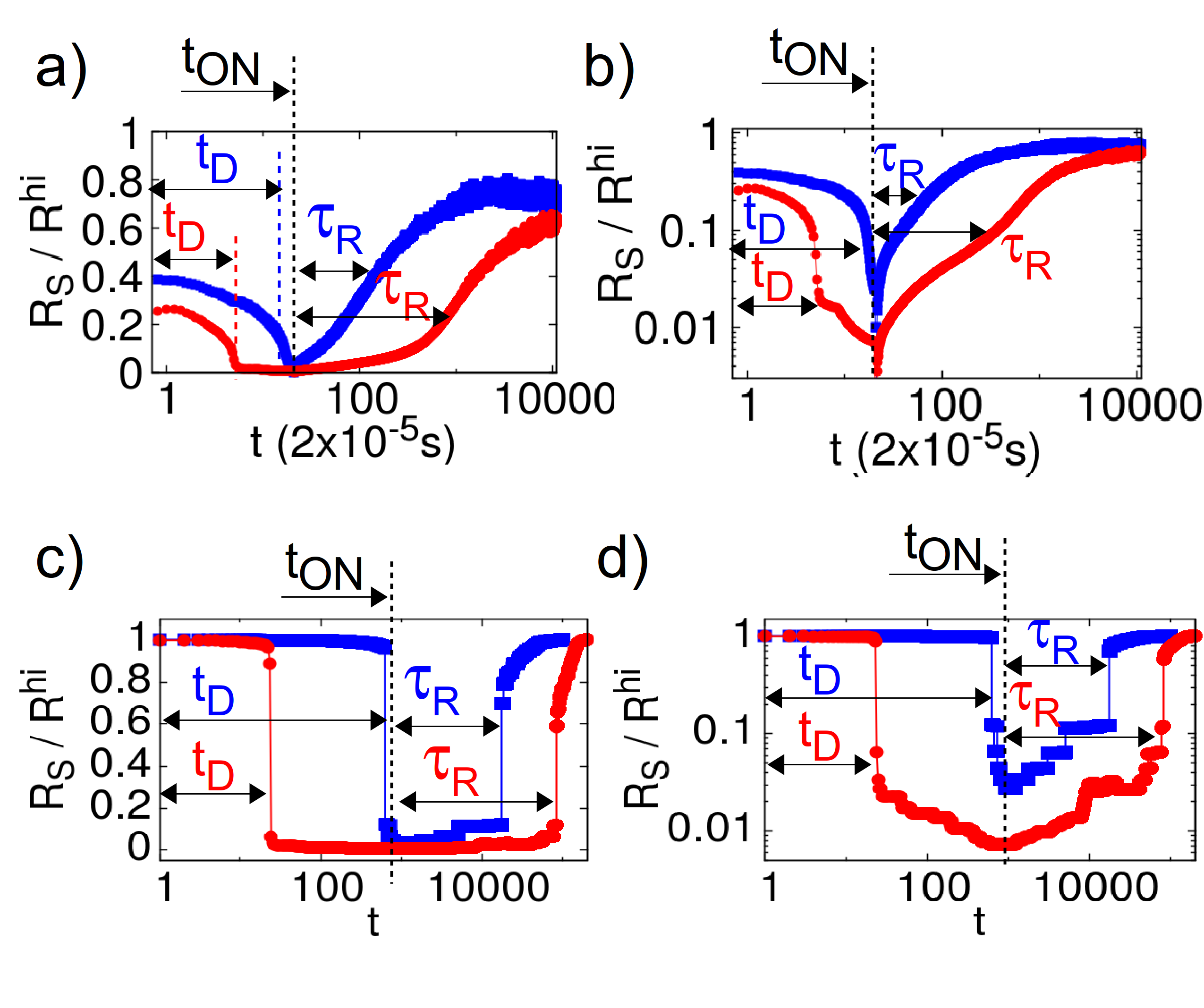
We may finally illustrate the behavior of the model upon the application of a train of voltage pulses. We show in Fig.13 the comparison of our model simulations with actual experimental data of the resistive change in a crystal of GaV4S8 upon application of voltage pulses. Two types of pulse protocol are applied: either a single pulse or a train of identical pulses with a relatively long separation, which mimics a train of spikes that may be arriving to the dendrites of a neuron Stoliar et al. (2017). In actual situations the arrival of pulses is mostly random, though here we focus on regular trains for the sake of simplicity. In the top panels of the figure we show the experimental data and in the bottom the simulations. Each pulse of the train is identical to the single one. The data in red color corresponds to the applied voltage and the data in blue to the respective resistance value . The small subpanels at the right of the main panels indicate the asymptotic value of the resistance after the voltage pulse protocol is terminated. In the experimental data we observe that the single pulse is sufficient to produce a resistive change, which takes place after about . However, this low-resistance state is volatile, as the corresponding asymptotic value has returned to the original high resistance value. In contrast, as the data of the right panel show, the application of identical pulses was enough to dramatically increase the retention time. Thus, seven pulses are found to be sufficient to drive the resistance change non-volatile (in the time scale of the experiment).
In the bottom panels we see that the simulations capture qualitatively well these effects. From the discussions of previous sections we can understand the behavior. As shown in the left panels of the figure, a single pulse is enough to induce an EMT with filamentary formation. However, that single pulse only produced a thin filament with a short retention time, which got rapidly reabsorbed. Thus the system returned back to the initial high resistance state. In contrast, the train of multiple pulses produced the gradual thickening of the filament, with a consequent much longer retention time and persists beyond .
This behavior may be considered an initial step towards the modeling of a recovery period of an artificial neuron under spiking stimulus. It may be interesting to mention that this variations in the recovery time may find potential useful applications in neural networks for tasks such as neural coding Rieke et al. (1999); Gerstner et al. (1997).
We may note that the inter-pulse time duration (s in the experiment) provides a rough indication of the reabsorption time of the filaments. The systematic investigation of the retention time with the parameters of the applied voltage pulsing protocol is an important issue but it certainly involves some technical challenges and is outside the scope of the present study.
.7 Conclusions
In the present study we have extended a model for the EMT to incorporate electro-elastic effects. This feature lead to spatial correlations in the growth patterns of filamentary structures in the resistive transition. In particular, it leads to the thickening of the filaments during longer applied pulses or multiple pulses. The increased thickness of filaments was directly related to a dramatic increase in retention time of the low-resistance state.
We should mention that our model does not predict any sharp or discontinuous transition between the experimentally observed volatile regime (ii) and the non-volatile regime (iii) discussed in the introduction. Nevertheless, it does indicate that the retention times may be exponentially increased by means of the applied pulsing protocol. Specifically the strength, duration and inter-pulse time, which may be tailored to optimize the growth and thickening of the filaments. The results of the previous section may be considered as an initial step in that direction. However, it should be realized that there are a large number of variables to take into account and the systematic investigation remains an important experimental challenge.
We also briefly refer to the qualitative similarities of our present model study and the behavior of spiking leaky-integrate-and-fire neurons. We are aware of the relative simplicity of our system with respect to the biological ones but, nevertheless, this may be taken as a contribution towards future implementation of neuromorphic electronic systems. In this regard, it is very exciting to envision that strongly correlated Mott materials may realize unexpected bio-inspired functionality.
References
- Mallat (2012) S. Mallat, Communications on Pure and Applied Mathematics 65, 1331 (2012).
- Schmidhuber (2015) J. Schmidhuber, Neural Networks 61, 85 (2015).
- Rozenberg (2011) M. Rozenberg, Scholarpedia 6, 11414 (2011).
- Janod et al. (2015) E. Janod, J. Tranchant, B. Corraze, M. Querré, P. Stoliar, M. Rozenberg, T. Cren, D. Roditchev, V. T. Phuoc, M.-P. Besland, and L. Cario, Advanced Functional Materials 25, 6287 (2015).
- Wong et al. (2012) H.-S. P. Wong, H.-Y. Lee, S. Yu, Y.-S. Chen, Y. Wu, P.-S. Chen, B. Lee, F. T. Chen, and M.-J. Tsai, Proceedings of the IEEE 100, 1951 (2012).
- Tang et al. (2016) S. Tang, F. Tesler, F. G. Marlasca, P. Levy, V. Dobrosavljević, and M. Rozenberg, Phys. Rev. X 6, 011028 (2016).
- Jo et al. (2010) S. H. Jo, T. Chang, I. Ebong, B. B. Bhadviya, P. Mazumder, and W. Lu, Nano Letters 10, 1297 (2010).
- Pershin and Ventra (2010) Y. V. Pershin and M. D. Ventra, Neural Networks 23, 881 (2010).
- Pickett et al. (2013) M. D. Pickett, G. Medeiros-Ribeiro, and R. S. Williams, Nature Mat 12, 114 (2013).
- Stoliar et al. (2017) P. Stoliar, J. Tranchant, B. Corraze, E. Janod, M.-P. Besland, F. Tesler, M. Rozenberg, and L. Cario, Advanced Functional Materials 27, 1604740 (2017).
- Imada et al. (1998) M. Imada, A. Fujimori, and Y. Tokura, Rev. Mod. Phys. 70, 1039 (1998).
- Stoliar et al. (2013) P. Stoliar, L. Cario, E. Janod, B. Corraze, C. Guillot-Deudon, S. Salmon-Bourmand, V. Guiot, J. Tranchant, and M. Rozenberg, Advanced Materials 25, 3222 (2013).
- Guiot et al. (2013) V. Guiot, L. Cario, E. Janod, B. Corraze, V. T. Phuoc, M. Rozenberg, P. Stoliar, T. Cren, and D. Roditchev, Nature Communications 4, 1722 (2013).
- Aoki et al. (2014) H. Aoki, N. Tsuji, M. Eckstein, M. Kollar, T. Oka, and P. Werner, Rev. Mod. Phys. 86, 779 (2014).
- Stoliar et al. (2014) P. Stoliar, M. Rozenberg, E. Janod, B. Corraze, J. Tranchant, and L. Cario, Physical Review B 90, 045146 (2014).
- Qazilbash et al. (2007) M. M. Qazilbash, M. Brehm, B.-G. Chae, P.-C. Ho, G. O. Andreev, B.-J. Kim, S. J. Yun, A. V. Balatsky, M. B. Maple, F. Keilmann, H.-T. Kim, and D. N. Basov, Science 318, 1750 (2007).
- Dubost et al. (2013) V. Dubost, T. Cren, C. Vaju, L. Cario, B. Corraze, E. Janod, F. Debontridder, and D. Roditchev, Nano Letters 13, 3648 (2013).
- Camjayi et al. (2014) A. Camjayi, C. Acha, R. Weht, M. G. Rodríguez, B. Corraze, E. Janod, L. Cario, and M. J. Rozenberg, Phys. Rev. Lett. 113, 086404 (2014).
- Georges et al. (1996) A. Georges, G. Kotliar, W. Krauth, and M. J. Rozenberg, Rev. Mod. Phys. 68, 13 (1996).
- Strogatz (2000) S. H. Strogatz, Nonlinear Dynamics and Chaos (Westview Press, 2000).
- Wilkinson et al. (2006) A. J. Wilkinson, G. Meaden, and D. J. Dingley, Ultramicroscopy 106, 307 (2006).
- Rieke et al. (1999) F. Rieke, D. Warland, R. de Ruyter van Steveninck, and W. Bialek, Spikes : exploring the neural code (MIT Press, Cambridge, MA, USA, 1999).
- Gerstner et al. (1997) W. Gerstner, A. K. Kreiter, H. Markram, and A. V. M. Herz, Proceedings of the National Academy of Sciences 94, 12740 (1997).
I Supplemental Material
II Dynamical Analysis and filament formation
In this section we complement the dynamical analysis of the model made in the maintext. We present a numerical integration of the model equations that By definition, the threshold voltage is the minimum one at which at least one filament is formed. In our description each filament is independent from each other, so the analysis is done studying a single-filament dynamics. To begin we notice that in our model the change in the number of conductive cells at time is given by the net rate equation of cell metalization (see maintext):
| (14) |
where is the number of metallic sites in the filaments at time and the number of sites (with , being N the total number of sites in a filament) and where we assumed that is at this point approximately the same for all sites in a given state (valid for , as explain in maintext). For simplicity we take and and we will start assuming . When the right-hand side of Eq.14 becomes zero then the rate of metalization is zero and the system is said to have a “fixed point”, which represents an equilibrium state of the system. In maintext, geometric solutions of this equation are shown for different applied voltages and the existence of a saddle-node bifurcation is shown Strogatz (2000). Here we analyze the dynamics of the system via direct numerical integration. In Fig.14 the integration of Eq.14 with a 4th order Runge-Kutta method is shown. Here we assume that the voltage applied on the sample is independent of time (valid for ), and that the drop of voltage on each cell is given by . Each panel in Fig.14 correspond to a different applied voltage. And each curve inside a panel correspond to a different initial condition (different initial ). Here we used that each filament has total length of and . In this plot we can see the evolution of the two fixed points: the “attractor” point (represented with a filled circle) and the “repulsive” point (represented by an empty circle). We can see again how the two points gets closer to each other as the voltage is increased, then collapse (at ) , and then no fixed points are present. The different initial conditions curves are meant to show the location and character of each fixed point: the system diverges from the “repulsive” point and converges toward the “attractor” point. The actual “physical” case would correspond to an initial close to zero, as the experimental devices begin in an insulating phase. For ( ) it can be seen that, before diverging, the system spends a significant amount of time at (close to where the fixed point was placed right before the bifurcation). This time-delay effect, known as the “ghost” of the fixed point, is a regular feature of saddle-node bifurcations and correspond to what we call in the maintext.
III Filaments size Distribution in Experiments
In Fig.15 we show the full distribution of metallic cross sections obtained from the scanning tunneling microscopy (STM) shown in Fig.7.b of maintext. The image correspond to a cleaved surface of a GaTa4Se8 compound after the EMT. The total area of the sample is of about x .
IV Retentivity for clusters with
In a filament of thickness greater than range of interaction () we can have two types of cells: the ones in the center and the ones in the “border”. Each type will have a different energy . For simplicity we will consider here the case of a n.n. interaction (where ). In this case the cells in the border have three CM neighbors and one MI from where (see maintext). And the ones in the center have 4 CM neighbors from where . Using the EMT rate equation we can find the mean lifetime of each layer (central or superficial) and . If then the filament will tend to relax from outside-in (starting from the surface towards the bulk) as explained in maintext. After one cell in the surface turns MI then its nearest inner-neighbor becomes superficial, and after it relax the next neighbor becomes superficial and so on. Then the rupture of a filament of thickness can be thought as the consecutive rupture of superficial cells (considering that the process begins at both boundaries of the filament with equal probability):
| (15) |
being the retentivity time of the filament and a factor related with the geometry of the de-percolation path (i.e. shape and size of the outer-in perforation) In maintext the evolution of as function of the thickness obtained from the simulations is shown, together with fit according to Eq.15. For the fit we fixed (according to the retentivity obtained for ) and used as a free parameter, obtaining .
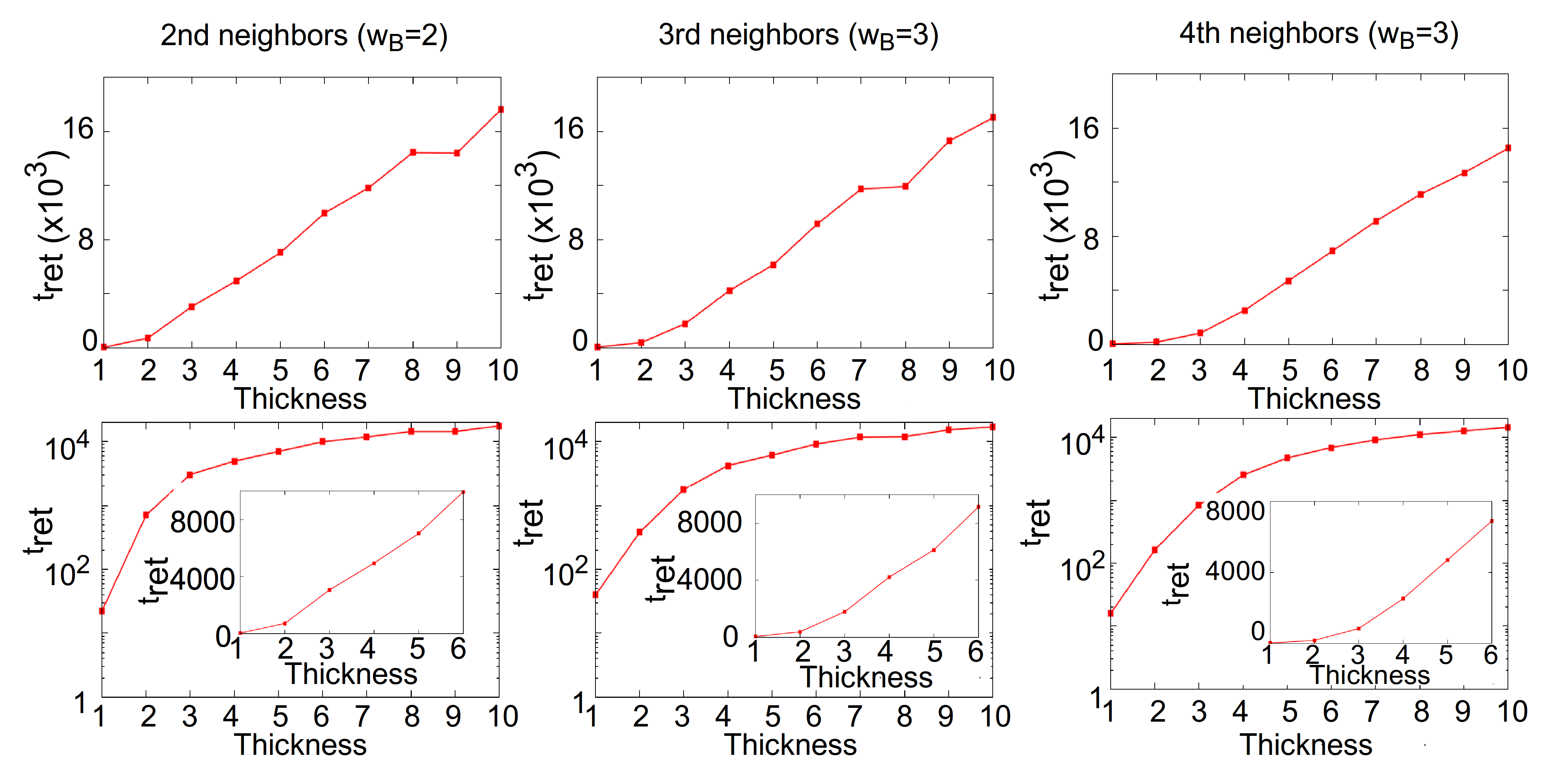
For a general the description is completely analogous. In the next section we present the results for longer interactions, ranging from 2nd neighbors to 4th neighbors.
V Longer range interactions
In this section we present simulations for longer interactions (beyond the n.n. used in maintext). In Fig.16 we show the results with interactions ranging from the 2nd to 4th layer of neighbors. In this case we can see that the evolution of as a function of the thickness exhibits first an exponential regime whose extension depends on the corresponding . After this the expected linear behavior can be seen as explained in maintext and in this supplement. To keep the variation of the energy (and so ) in the same range of magnitude for every interaction (due to computation times), we used a different surface constant () for each case. We used , and for the 2nd, 3rd and 4th neighbors interaction respectively.