Reversible Fluxon Logic: Topological particles allow ballistic gates along 1D paths
Abstract
As we reach the end of Moore’s law, digital logic uses irreversible logic gates whose energy consumption has been scaled toward a lower limit. Reversible logic gates can provide a dramatic energy-efficient alternative, but rely on reversible dynamics. Here we introduce a set of superconducting reversible gates that are powered alone by the inertia of the digital input states, contrasting existing adiabatic prototypes which are powered by an external adiabatic drive. The classic model of an inertia-powered reversible gate uses ballistic particles which scatter in 2D, where the digital state is represented by the particle path. Our ballistic gates use as the bit state the topological charge (polarity) of a fluxon moving along a Long Josephson Junction (LJJ) such that the particle path is confined to 1D. The fundamental structures of our Reversible Fluxon Logic (RFL) are 1-bit gates which consist of two LJJs connected by a circuit interface that comprises three large-capacitor Josephson junctions (JJs). Numerical simulations show how a fluxon approaching the interface under its own inertia converts its energy to an oscillating evanescent field, from which in turn a new fluxon is generated in the other LJJ. We find that this resonant forward-scattering of a fluxon across the interface requires large capacitances of the interface JJs because they enable a conversion between bound-evanescent and traveling fluxon states (without external power). Importantly, depending on the circuit parameters, the new fluxon may have either the original or the inverted polarity, and these two processes constitute the fundamental Identity and NOT operations of the logic. Based on these 1-bit RFL gates, we design and study a related 2-bit RFL gate which shows that fluxons can exhibit conditional polarity change. Energy efficiency is accomplished because only a small fraction of the fluxon energy is transferred to modes other than the intended fluxon. Simulations show that over of the total fluxon energy is preserved during gate operations, in contrast to irreversible gates where the entire bit energy is consumed in bit switching. To provide insight into these phenomena, we analyze the 1-bit gate circuits with a collective-coordinate model which describes the field in each LJJ as a combination of fluxon and mirror antifluxon. This allows us to reduce the many-junction circuit (the 3 interface JJs and the many JJs approximating the LJJs, solved numerically) to that of two coupled degrees of freedom that each represent a particle. The evolution of the reduced model agrees quantitatively with the full circuit simulations and validates the use of the mirror-fluxon ansatz. Parameter tolerances are calculated for the proposed circuits and indicate that RFL gates can be manufactured and tested.
I Introduction
Today’s conventional digital logic is based on irreversible gates. Physically, the irreversibility arises in a gate due to the energy that is dissipated in switching processes between the states representing the logic bits. This energy cost is generally set by the energy of the digital state itself: the charging energy of a voltage state in semiconductor logic or the magnetic energy of a flux state in conventional superconducting logic. In both cases, sufficiently large damping ensures deterministic and fast state switching compatible with GHz processing speeds. Unlike CMOS gates, however, the intrinsic damping in superconducting circuits is very small, allowing nearly dissipationless reversible dynamics. As a result, superconducting circuits also allow for the implementation of both quantum logic and reversible digital logic. The most common type of reversible digital logic is “adiabatic reversible logic”, where state switching uses an external waveform (or clock) to steer an adiabatic state evolution in the absence of large damping. Here we report on an unusual gate class known as ballistic reversible gates, which are powered by the inertia of the incoming bits. Specifically, we find that fluxons can undergo energy conserving transformations of polarity and this mechanism can be used for ballistic reversible logic gates.
Industrial development of microelectronics has long benefitted from transistor density scaling which allows the vast improvements described by Moore’s law. However, the related performance scaling has slowed down considerably in recent years and is expected to come to an end soon. One particular limiting factor is the heat generated during CMOS transistor switching in logic gates IRDS2017 ; TheWon2017 . These logic gates are irreversible from an information perspective because they do not perform one-to-one maps of input-to-output states. Their energy cost includes Landauer’s entropy cost of for the erasure of each bit of information at temperature . Though the bit switching energy of irreversible gates could in principle be this small, in practice it consumes the entire energy of the bit state itself (e.g., the voltage state) through fast damping in order to enable GHz processing speeds. For reasons that include thermal stability and state distinction, the bit state energy has to be (e.g., ), and consequently the switching energy exceeds Landauer’s entropy cost by orders of magnitude in practice. Similar principles hold for conventional single-flux quantum (SFQ) logic in superconducting circuits. SFQ logic uses a flux quantum generated by a persistent current in a quantizing loop to represent one bit state. Bit switching, i.e. the change of the flux state in the loop, is enabled by a Josephson junction (JJ); once the total current acting on a JJ exceeds its critical current , it undergoes a rapid -phase change. Equilibrium is reestablished through a damping resistor that shunts the JJ LikSem1991 . Similar as in the CMOS bit switching, the dissipated energy here is on the order and larger than the bit energy of the flux quantum itself; specifically, the switching energy is , where is the superconducting flux quantum. One such recently developed (irreversible) SFQ logic type HerrETAL2011 ; PrivComm2017 ; Holmes2013 allows -phase switching at an energy of only .
Reversible logic gates provide an alternative approach to computing. These gates produce no entropy related to bit-erasure, since they perform one-to-one mapping of input-to-output states. A corresponding theoretical model for a reversible computer was established decades ago Bennett1973 . To provide an advantage over irreversible logic, reversible gates must use dynamics that conserves most of the bit-state energy. This can be achieved within an adiabatic model, developed by Likharev Lik1982 in 1982, by using externally applied fields that adiabatically modulate the circuit potential. Arriving later than their quantum counterparts in superconductivity, reversible digital logic has been demonstrated more recently in circuits, which include N-SQUID RenSem2011 and reversible QFP QFPgate . According to Likharev’s adiabatic model, energy dissipation varies proportional to the modulation frequency Lik1982 ; YoshikawaETAL2015 and thus can be made arbitrarily small as the speed is lowered.
Though demonstrated reversible gates are of the adiabatic (reversible) logic type, a physically distinct type known as ballistic gates can be studied. These make use of scattering processes and are solely powered by the initial energy of the digital state. This is apparent in the original “billiard ball model” FredTof1982 : particles moving under their inertia collide with each other and with reflective boundaries of a well-defined 2D gate geometry. The resulting paths taken by the particles encode the digital output state of the gate. Ballistic gates have been studied using soliton propagation within fibers IslSoc1991 or 2D layered media SchOre2005 . A technical challenge in this type of reversible logic is that they must be correctable for path perturbations in 2D and desynchronization errors DruMan1994 , and here we will address the former.
In this work we introduce gates for efficient ballistic reversible logic in superconducting circuits under the name of Reversible Fluxon Logic (RFL). This approach uses fluxons and antifluxons in Long Josephson junctions (LJJs) to represent the two bit states. A fluxon – or flux-soliton – is a spatially extended topological excitation of the LJJ and carries a quantized magnetic flux ( in case of an antifluxon). In RFL the LJJs form fluxon-waveguides and are connected at circuit-interfaces. Fluxon gates can be made of these structures where a fluxon scatters from one LJJ to another through a resonant nonlinear process. Through numerical simulation of the gate circuits we find cases where an incoming fluxon exites resonant dynamics of the coupled LJJs which results in the net forward scattering of the fluxon to another LJJ. In these nonlinear processes the character of the incoming fluxon changes near the interface where it turns into a localized interface excitation with evanescent fields in the LJJs. From this localized state a new ballistic fluxon forms afterwards in the other LJJ. For this 1D scattering no path corrections are required in contrast to the original (2D) ballistic gate model.
Importantly, while the fluxon number is conserved, the scattering can result in the transformation of a fluxon into an antifluxon (or vice versa), and this change of polarity provides a means for bit-switching (defined as a NOT gate). This is fundamental because the fluxon polarity represents a topological charge which cannot change in a planar LJJ (only along a LJJ that is twisted in 3D). The NOT gate occurs in a 1-bit structure which has three JJs in the interface. For different parameters of these interface JJs the dynamics changes; in particular the gate type can be changed to an Identity (ID) gate, where fluxon polarity is preserved but the resonance is changed. In related 2-bit gates the fluxon polarities induce a conditional polarity change. The bit-switching in RFL involves a (gradual) undamped -phase change of an interface JJ. The change is thus found to be enabled by resonance between LJJs, and it contrasts adiabatic reversible logic which generally uses a phase change, related to neighboring minima of the JJ potential Lik1982 .
The RFL gate interface is designed to ensure that an incoming fluxon (with a given velocity and for given LJJs) is coherently transformed into the local interface excitation and back into another forward-moving fluxon in a different LJJ. To accomplish this, the ends of the LJJs near the interface must behave differently than in bulk. In particular we find that relatively large (added shunt) capacitances of the interface JJs are crucial to the resonant scattering present in the 1- and 2-bit gates. We have designed the RFL gates for relatively high incoming fluxon velocities of around , where is the upper (relativistic) velocity limit.
The RFL gates presented in this study are reversible in the sense that their energy cost is only a small fraction of the digital state energy. In our simulations an output fluxon can obtain of the energy of the input fluxon. The gates can also be logically reversible at lower efficiency, which allows some tolerance to imperfect structures. The remaining small fraction of initial energy is dissipated to the environment of the gate in the form of small-amplitude plasma waves in the LJJs. The JJs in the simulations are undamped. Beyond this general property of superconducting circuits, we note that the observed high energy retention in the fluxon degree of freedom is a speciality of our resonant logic gates. Also, the RFL gates have a gate time of only a few Josephson oscillation periods, , where is the natural frequency in the LJJ. In principle could be on the order of tens of GHz for fast processing speeds.
The complex scattering dynamics observed at the circuit interfaces in an RFL gate goes beyond the usual fluxon perturbation theory McLaughlinScott1978 . While the latter assumes the fluxon’s integrity (possibly allowing for internal excitations, shape modes, etc.) in our case the fluxon breaks up at the interface and its energy is converted into an interface oscillation mode. This mode involves an excitation of the interface JJs but also has finite amplitude in the adjacent LJJs, decaying away from the interface. The LJJs therefore play a role not only as input and output ports, but also as integral parts of the gate itself. To analyze the non-perturbative scattering dynamics we parametrize the fields in each LJJ as a superposition of a fluxon paired with a mirror antifluxon. This collective coordinate (CC) model can account for the various scattering processes with conserved energy, including those where the fluxon polarity changes. In case of the 1-bit RFL gates, for example, the Lagrangian produces coupled dynamics in 2 coordinates. The dynamics can thus be thought of as a possible excitation in one LJJ interacting with a possible excitation in the other LJJ, where each has an independent spatial coordinate along its LJJ. The CC dynamics accurately reproduces dynamics from the full gate simulation. The forward-scattering with and without polarity change are seen to arise from the special form of the effective potential and essential mass-gradient forces generated by the interface. The mass-gradient forces, not used in other SFQ logic, are introduced in our superconducting digital gates through engineered capacitances.
The interface scattering of the fluxon may be compared with scattering of a fluxon at a point defect in an LJJ FeiKivVaz1992 ; GooHab2007 , or at a qubit-generated perturbation potential AveRabSem2006 ; UstinovETAL2014 ; AnnaFluxon ; KuzminETAL2015 . In those situations the moving fluxon interacts with a small-amplitude bound state at the defect. Above a critical velocity the fluxon is transmitted, but a slow fluxon may be back-scattered or trapped. Unlike in these systems, our system allows polarity change of a fluxon. This is here made possible since one of the superconducting electrodes of the LJJ is interrupted in the interface by a JJ. This JJ can undergo large phase winding in resonance, corresponding to a change of the flux inside the LJJ, e.g. by two flux quanta in case of the NOT gate. Moreover, we typically find that the outcome of scattering at the interface depends only moderately on the incoming velocity, in contrast to fluxon scattering at point defects for which high sensitivity to the incoming fluxon velocity had been found FeiKivVaz1992 .
Building on the results for the 1-bit gates, we have also designed and simulated 2-bit gate structures which are found to allow conditional polarity changes for the two incoming fluxons. In this particular 2-bit gate, a NSWAP, the coupled dynamics of the two input fluxons is symmetry-related to the dynamics of two different uncoupled 1-bit gates. Depending on the relative polarity of the two input fluxons it conditionally produces a NOT or ID operation. This 2-bit gate has an interface with 7 capacitance-shunted JJs. The present work covers an initial set of RFL gates. Subsequent work describes how to store and launch fluxons for the purpose of synchronization and resupply of energy between gates WusOsb2018 . Ref. WusOsb2018 also uses a 2-bit gate named IDSN with similar dynamics as in the here presented gates, as a key component of an efficient CNOT gate.
The paper is organized as follows: In Sec. II we introduce the gate circuit and briefly describe the main results for the fluxon logic gates. We start by presenting numerical simulations of circuits with fluxon dynamics in the 1-bit gate structures. We then analyze the fluxon dynamics in these gate structures by means of a collective coordinate (CC) model. It describes the fields near the interface as consisting of a fluxon paired with a mirror antifluxon (Sec. II.3). From two 1-bit gate types we then construct a 2-bit gate which likewise is unpowered and reversible (Sec. II.4). We further study dynamics of the 2-bit gate embedded into a simulation test platform for fluxon launch and output state storage. This serves to show that the gates do not depend sensitively on a perfectly launched fluxon. Section III presents more detail on the CC model and its application to describe the fluxon scattering at the circuit interfaces, including such scattering that is not used for gates. This analysis provides a better intuition for the scattering dynamics and helps to identify the relevant parameter regimes for the gates. The precise interface parameters used in gates are calculated numerically in Sec. IV from a Monte-Carlo optimization of parameters. The gate operation under changes of single parameters is calculated as well (parameter margins). In Sec. V we explain in detail the operation of the 2-bit gate and how it can be mapped to equivalent 1-bit gates, as it depends on the relative polarity of input fluxons. A conclusion is given in Sec. VI. The appendix contains details of the gate analysis and shows that we expect negligible energy loss from fluxons in our LJJs due to the small LJJ-model discreteness.
II Operation and analysis of gates
II.1 1-bit gate system
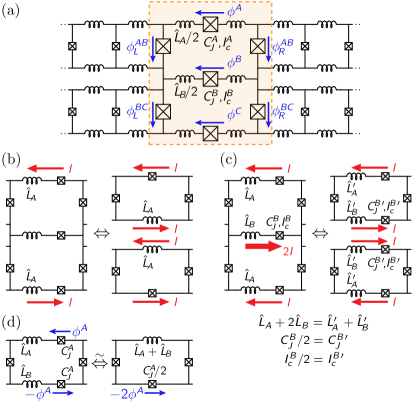
We study the dynamics of a fluxon in a superconducting circuit as sketched in Fig. 1(a). It consists of two discrete LJJs at . These are made from an array of Josephson junctions (JJs), with parallel critical current and capacitance , connected to their neighbors through cell inductance . Each LJJ ends at an interface Josephson junction of capacitance and critical current (). The termination junctions (, ) of two LJJs are connected in a series loop with two other elements: a central interface junction of (, ), and an inductor . Elements (, ), (, ) and with their connections constitute the interface cell.
We simulate the dynamics by numerically integrating the equations of motion for the junction phase differences: for the center interface junction, and for the and junctions in the left and right half of the circuit, respectively, where the phases of the left and right interface junctions are and . The equations of motion are generated by the Lagrangian
As defined above, there are identical junctions (, ) and inductors, , in the LJJ cells. Also, the left and right interface junctions have and . Finally, the interface inductance and center junction have values and (, ), respectively. The currents on the upper rail of the LJJs are given by (, ) and on the lower, where is the total inductance of the –th LJJ cell. The current on the upper rail in the interface (with center inductor ) is given by , where is the current on the lower rail of the interface. The interface cell is symmetric in propagation direction (left–right), as required for a physically reversible gate.
When scaling the parameters , in the limit a continuous LJJ is realized rather than our approximate one. The dynamics of the continuous LJJ are governed by the sine-Gordon equation (SGE) DauxoisPeyrard__PhysicsOfSolitons ; McLaughlinScott1978 ; Newell ,
| (2) |
The characteristic time and length scales of the LJJ are given by the Josephson frequency and Josephson penetration depth , defined by and , where and are the LJJ inductance and critical current per unit length . The upper bound for the group velocity in the LJJ is the Swihart velocity .
In the (infinite) continuous LJJ a stable fluxon exists in form of the soliton solution to the SGE, with the phase and phase-derivative profiles
| (3) | |||||
| (4) |
where is the voltage across the LJJ. We choose the range , and the polarity () for a fluxon (antifluxon) solution. Here is the center position of the fluxon, which propagates with constant velocity () and has a characteristic width .
For use in a logic gate, a fluxon first needs to be created in an LJJ. In this context, Fig. 1(e) shows a schematic of a simple test platform for a 2-bit gate, with two input and two output LJJs (the 2-bit gate is discussed in Sec. II.4, and in more detail in Sec. V). In addition to the 2-bit gate itself, the platform provides components that allow one to (i) create ballistic fluxons in the input LJJs from coupled transmission lines and (ii) store flux at the end of each LJJ output for a gate readout (test). The fluxon launch in each input LJJ is initiated by ramping up the input voltage of a transmission line. Also, in the platform the LJJs and interface are additionally coupled via small capacitances to ground. We have successfully simulated the fluxon launch and the subsequent gate operations and flux storage of this test platform, as discussed in Sec. II.4, cf. Fig. 6. In the interest of simplicity, simulations presented here are mainly performed only for the gate alone, without circuit components for launch, output flux storage, and capacitive coupling to ground.
In these simulations, a soliton is simply taken as the initial condition, . This is evaluated on the discrete lattice of the circuit, (), where is the lattice spacing. Specifically, a fluxon is initialized in the left LJJ, , and is incident on the interface with initial velocity , and polarity .
In an ideal continuous LJJ the fluxon energy, , is conserved according to the SGE, where . In a discrete LJJ the fluxon motion is in general damped, because the discreteness forms a perturbation through which a moving fluxon can excite linear plasma modes of the (discrete) LJJ. (These wave modes are solutions of the linearized SGE.) The moving fluxon thus emits plasma waves and as a result loses energy BraunKivshar1998 ; UstinovETAL2008 ; PeyKru1984 . However, this energy loss mechanism is strongly suppressed if , and this criterium characterizes the regime of ‘small LJJ discreteness’. The LJJs used in this paper as part of the logic gates are chosen in this regime, , where the energy loss of the moving fluxon is negligible. In App. A we briefly discuss the fluxon-energy loss-rate at this (small) discreteness and its dependence on the initial fluxon velocity. For a typical initial velocity, , the fluxon energy is , where of is kinetic energy. As shown in App. A, in our LJJs such a fluxon loses only a fraction of its energy in a time due to the discreteness. This allows us to discuss the LJJs as nearly continous in the context of the RFL gates, which are meant to operate over such short times.
II.2 Fluxon forward scattering for 1-bit gates
The gate circuit of Fig. 1(a) supports equilibrium states of the form in the LJJ and on the center interface JJ, where and is the Heaviside step function. Since we constrain studies to a parameter regime with , without loss of generality we can disregard states with finite flux trapped in the interface cell Barone , such that in equilibrium. Taking as the initial state, in fully inelastic scattering of an input fluxon, i.e. if the entire initial fluxon energy is exhausted in the interface region, the interface would settle into the equilibrium state . Inelastic scattering generally results from excitation of high-frequency plasma waves () at the interface which are radiated into the LJJs and thus spread the initial fluxon energy incoherently. The amount of radiation generated at the interface depends on the interface parameters. It is strongly suppressed in the following regimes, related to known scattering dynamics in an LJJ: (i) The fluxon is transmitted across the interface for and , while , , , because the center interface junction essentially acts as a small linear inductance due to the large , and the entire circuit thus approximates a single LJJ. (ii) If the potential energy of the interface is too high, e.g. , the fluxon is reflected back before reaching the interface, similar to a shunt-terminated LJJ. (iii) The inter-LJJ coupling is suppressed due to the small and if , , , and . This is comparable to an open terminated LJJ and thus the incident fluxon is scattered back elastically as an antifluxon, while the center interface junction undergoes a -phase winding. (Note that the interface cell does not store significant flux, but 2 flux quanta, , must be exchanged between the interface cell and the environment.) These elastic processes involve transitions of the initial equilibrium state in the interface region to (i) , (ii) , and (iii) , respectively.
Inelastic scattering and fluxon reflection are undesirable for efficient reversible gates. We therefore mainly report on reversible scattering phenomena where the fluxon energy is transferred into a coherent localized oscillation about the equilibrium state , and remarkably followed by the creation of a fluxon or antifluxon in the other LJJ as a resonant forward-scattering process.
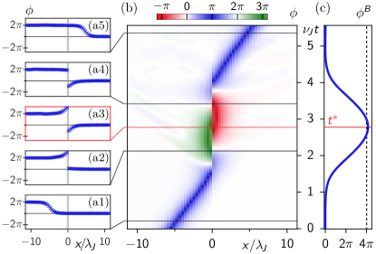
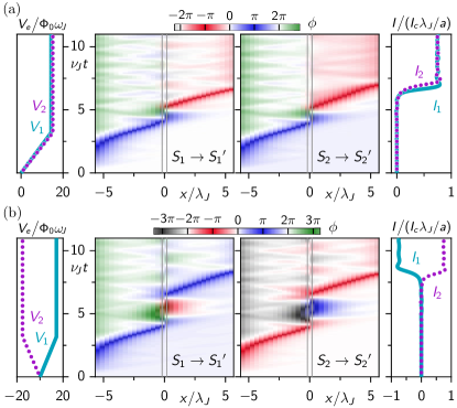
In Fig. 2(b) numerically simulated dynamics of the LJJ phases are shown vs. position and time , for interface parameters given in the caption. The phases are also shown for specific times in Fig. 2(a1-a5). After moving ballistically (approximately freely) in the left LJJ, e.g. panel (a1), the fluxon energy is converted to a localized oscillation at the interface with evanescent fields into the LJJs, e.g. panels (a2-a4). During that stage the characteristic phase-profile of the original fluxon, Eq. (3), is destroyed. A large phase difference has accumulated between the left and right interface junctions, and . This is accompanied with an increase of the phase of the center interface junction, shown in Fig. 2(c), such that the phase across remains small, . During the localized oscillation, the field , measured relative to the equilibrium state , behaves parity-time antisymmetric where the symmetry time is defined by . After the symmetry time we observe the energy from the local oscillation create a ballistic (unpowered) moving fluxon in the right LJJ (a5), while the interface region is left in the equilibrium state . The process is almost ideally elastic, with the new fluxon propagating at of the initial velocity , and we note that no bias is present in the gate region (within several Josephson penetration depths of the interface). Compared to straight transmission across the interface the new fluxon appears with a time-delay of , within a factor of three of the Josephson period.
A different reversible forward-scattering is illustrated in Fig. 3, for an interface that differs from that in Fig. 2 only by increasing to . Coherent energy transfer again takes place from the incident fluxon to an interface oscillation which spans a time , approximately half of the process in Fig. 2. The field exhibits parity-time symmetry with respect to a time defined by . Thus, after the oscillation the interface region settles to the state with , . Here a fluxon is emitted into the right LJJ, (a5), but in contrast to Fig. 2 it is an antifluxon (a fluxon with inverted polarity, ).
If the two fluxon polarities encode the bit states 0 and 1, these unconventional fluxon scattering phenomena implement 1-bit reversible gates. The process of Fig. 2 (Fig. 3) performs an ID (NOT) operation by preserving (inverting) the polarity of the input fluxon, during which only % (%) of the initial fluxon energy is dissipated. This results in a dissipation , much less than the potential energy (rest energy) of the fluxon .
The small energy difference between the input fluxon and the output fluxon is dissipated in form of plasma waves generated at the interface and radiated into the LJJs, see the faint wave patterns in Figs. 2 and 3. In addition to this loss mechanism we expect smaller losses from (superconductor) quasiparticles and dielectric loss; methods to control these mechanisms are known, even in qubits where the sensitivity is much higher to loss than our gates.
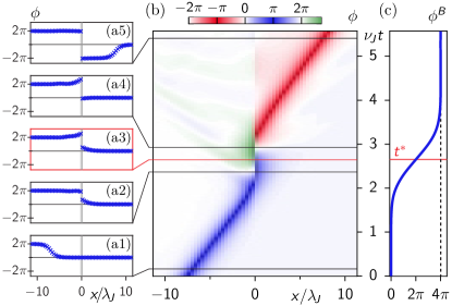
The interface parameters of Figs. 2 and 3 were chosen near numerically optimized values for the two respective gate types. The optimization studies are presented in Sec. IV. As described above, a conversion between the two gate types is here accomplished by adjusting the capacitance alone. Another parameter change has a similar effect, namely an increased can turn an ID into a NOT (compare Fig. 7(c2)). It is important to emphasize that each gate by itself is fully autonomous, requiring no drive fields, and is determined by the fixed circuit parameters alone. The efficient gate dynamics takes place on the time scale of the inverse plasma frequency .
These 1-bit gates operate with one fluxon (bit) at a time. Therefore the spacing required between fluxons must be greater than the sum of two terms. The first term is to avoid perturbations of the gate dynamics by a second arriving fluxon, and is given by the gate time multiplied by the velocity. The second term is related to possible interactions between consecutive fluxons because of their finite width. For our intended velocity () this width is .
The fluxon gates differ fundamentally from existing reversible logic where adiabatic drive fields RenSem2011 ; QFPgate slowly evolve the gate potential while at all times retaining the state close to the potential minimum Lik1982 . The fluxon gates also contrast conventional SFQ gates which dissipate the potential energy during damped switching from the high-energy state to the low-energy state.
II.3 Collective Coordinate Model
To understand these complex nearly-ideal elastic dynamics we employ a collective coordinate (CC) approach DauxoisPeyrard__PhysicsOfSolitons . Here we briefly sketch the method and start the analysis of the 1-bit gates above. More detail on the CC approach will be provided in Sec. III.
As an ansatz for the fields in left and right half of the circuit we choose
| (5) |
each consisting of a linear superposition of fluxon and mirror antifluxon fields, where is defined in Eq. (3). This conveniently parametrizes the possible asymptotic behavior of elastic scattering for our interest — for one incident fluxon of polarity (see insets of Fig. 7(a1)). Asymptotically, if the coordinate () is far away from the interface, the field in the LJJ , as defined in Eq. (5), can be either fluxon- or antifluxon-like, and we refer to it as a particle. We note that, even though the coordinate () can assume any value in , the left (right) particle energy is always localized within the real space of the left (right) LJJ, about (). For , the particle excitation vanishes. For example, an incident fluxon in the left LJJ is represented by , . Also, a fluxon (antifluxon) in the right LJJ is given by and (). From fits to the numerical solutions we find that Eq. (5) for also approximates the observed large interface oscillation (around the state ) during gate dynamics.
By inserting ansatz Eq. (5) in the system Lagrangian, Eq. (II.1), the many degrees of freedom reduce to the two collective coordinates . Using justifications above, we also constrain in the CC calculations, thereby eliminating the interface phase . This approximation is valid in a leading order perturbation expansion of the interface equations of motion, due to the small interface inductance , as fulfilled in the simulations of Figs. 2 and 3. We then obtain coupled equations of motion,
| (10) |
where the mass matrix is given in Sec. III. The diagonal mass matrix components (), describe the particle mass which varies near the interface (). The off diagonal mass (coupling) components approach zero away from the interface, with . The mass coupling is proportional to the center JJ capacitance , and this is a key to coupling between a particle in the left LJJ and the right one.
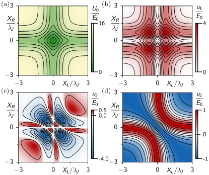
The potential is symmetric under the coordinate exchange and is of the form
| (11) |
Herein and have even parity under each of the transformations (), while has no parity symmetry. One potential landscape is shown in Figs. 4(a) and (b). These correspond to the ID and NOT gates of Figs. 2 and 3, respectively, and are identical since both gates have the same critical currents and . For either of , the potential forms four valleys, each corresponding to a single fluxon as described earlier. A central well exists at . Due to the interface potentials contribute only weakly to , and the valleys are therefore connected with the central well below the initial fluxon energy (gray equipotential line). Thus, in principle conservative scattering between valleys is possible. The gates of Fig. 4(a) and (b) differ by capacitance and thus mass matrix alone, but have identical CC potential with negligible -contribution. We note, however, that the parity-breaking contribution of can also be used to change the gate type from ID to NOT. This is done by increasing and is discussed in Sec. III.
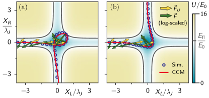
In Figs. 4(a) and (b) the CC trajectories are shown (red lines) for the ID and NOT gates, as obtained from integration of Eq. (10) with initial conditions , , and . These can be compared with trajectories obtained from accurate fits of the ansatz (Eq. (5)) to the numerical simulation data from Figs. 2 and 3 (blue markers). From the good agreement between the two we conclude that the CC equations of motion accurately produce the correct forward-scattering dynamics. In Fig. 4(a) the trajectory exhibits a net angular rotation of into the valley with , corresponding to a fluxon emitting into the right LJJ (ID gate); in Fig. 4(b) a -rotation of the trajectory into the valley with corresponds to the emission of an antifluxon (NOT gate). The trajectories evolve from initial conditions to , although no significant potential coupling exists between and due to negligibly small . The coupling is instead provided by the coupling mass in Eq. (10), stemming from the relatively large capacitance .
In the particle interpretation originating from the ansatz, an incident fluxon-like particle from the left LJJ changes its character at and also excites a particle in the right LJJ from , see 2nd diagram of Figs. 1(b1) and (c1) as well as panels (b2) and (c2). Finally, the left particle remains at , while the right one (initially at ) exits () with fluxon- or antifluxon-like character, see last diagram of Figs. 1(b1) and (c1). We will analyze these dynamics in detail in Sec. III.3, after giving more detail of the CC (Sec. III.1) and discussing general CC dynamics observed for different interface parameters (Sec. III.2).
The logic allows a comparison to billiard ball logic FredTof1982 , which ideally can perform reversible computing gates in two spatial dimensions (2D), using perfect hard collisions with barriers and each other. Standard scattering in a single sine-Gordon (or LJJ) system seems unlikely since there is only a delay from weak interactions between solitons (fluxons) which induces only time delays from ballistic collisions. However, our 1-bit fluxon gates introduce elastic collisions at the interfaces due to a strongly coupled interface between the LJJ, which are confined to 1D segments (LJJs). Rather than altering particle paths, as in the billiard ball model, they can change the particle type (polarity) during a collision. The collisions are accurately described by the above particle to particle collision. The excitations of an input particle from interacts with the other particle at , and induces scattering to .
II.4 2-bit gate
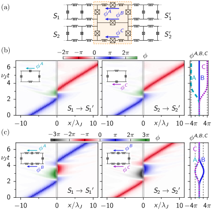
We next exploit the different 1-bit gate dynamics for the design of a conditional 2-bit gate, which depends on the interaction of the fields created by the input fluxons. This gate circuit is shown in Fig. 5(a). It has vertical mirror symmetry as well as mirror symmetry along the propagation direction (left–right). For optimized interface parameters, as given in the caption, near-elastic forward scattering takes place for synchronized input fluxons. Elastic behavior here implies that in both cases, equal and opposite polarity input, nearly all of the energy is returned such that the output velocity nearly equals the input velocity. The output depends on the polarities of the input fluxons: both undergo polarity inversion if they are of the same polarity, as shown in Fig. 5(b), but input fluxons of opposite polarity both retain their original polarities, as shown in Fig. 5(c). When encoding bit states by polarities this yields a controlled NOT(SWAP) = NSWAP gate – state pairs (0,0) and (1,1) are reversibly converted into each other, while state pairs (0,1) and (1,0) remain invariant. Similar to the 1-bit gates, only 2.1% of the initial fluxon energy is dissipated in any of the NSWAP operations. Also, with a change of the interface cell topology, through the use of wiring crossovers, the NSWAP is converted into a SWAP. We note that, even though such 2-bit gates could also be obtained by mere rerouting (wiring crossover), the NSWAP gate presented here is fundamentally different since it relies on the strong interaction between the bit states at the interface. This is the first discovered 2-bit gate of the fluxon logic type; other 2-bit RFL gates have been subsequently investigated WusOsb2018 .
The dependence of the interaction in the interface cell on the relative polarities of the input fields can be understood from the dynamical equivalence with 1-bit gates. We note that the value of here is similar to that of the previously presented 1-bit gates, which allows comparisons of the top or bottom part of the 2-bit gate to the previously discussed 1-bit dynamics. If the input fluxons have the same polarity the center interface current vanishes for symmetry reasons, and the center junction is not excited, . Here the dynamics of the upper and lower part of the interface are thus equivalent (see Fig. 5(b) insets) to two individual 1-bit interfaces, each with a center junction equal to the upper center junction (, ) of the 2-bit interface in Fig. 5(a). These parameters closely agree with those of the center junction of Fig. 3 and thus the dynamics correspond to a NOT gate for each input fluxon. On the other hand, if the input fluxons have opposite polarities the interface dynamics in the upper and lower part are effectively decoupled in another way. In this case, the upper and lower part of the interface are each dynamically equivalent to a 1-bit interface that has two center junctions rather than the one discussed previously (see insets to Fig. 5(c), compare also to Fig. 13). One of the equivalent center junctions is the same as the upper center junction of the 2-bit interface with values (, ). The second equivalent center junction must carry half the current of the 2-bit interface junction. As a consequence it must have values , in order to produce the same phase winding . The critical currents are small such that we neglect them for this discussion. We see from the the numerical values of our 2-bit gate that which explains that during the dynamics. It is intuitive to see that this can be approximately simplified further to a 1-bit interface with one center junction because the two center junctions are in series and thus act as a single interface junction with capacitance (also described in Fig. 10 below). This is in close agreement with Fig. 2, where the center interface junction has the capacitance . Therefore, as expected from analysis, the ID gate is generated for each of the input fluxons of opposite polarity.
Continuing the comparison with billiard ball logic started above, we see that interactions between fluxons allow them to switch their polarity conditionally, while billiard balls conditionally change their paths due to collisions. Here the length scale of the interaction is defined by the Josephson penetration depth . Furthermore, this 2-bit gate shares features with 1-bit gates, such as large center-interface capacitance which allows the oscillatory dynamics for reversible and non-dissipative fluxon gates.
Finally we have tested the NSWAP gate in a realistic test platform, as shown in Fig. 1(e). Figure 6 shows the results of the simulation. A fluxon is launched by ramping up the external voltages of transmission lines which are inductively coupled to the input LJJs. The gate parameters are identical to those in Fig. 5, however a ground plane is simulated by adding a stray capacitance to ground at each side of a junction, with a value . The larger phase fluctuations relative to the simulations of Fig. 5 are related to small LJJ dimensions (each LJJ consists of 14 JJs), capacitive coupling to ground (while interface not optimized under this condition), and small imbalance between external voltages (). In this test platform the output fluxons are stored in loops with large inductance while parallel resistances allow the fluxons to quickly create persistent currents in the storage loops. This test platform simulation shows the same fluxon logic despite non-ideal launch conditions (including non-equal waveforms and short left-hand side LJJs) and non-optimized gate (created by added ground plane capacitance).
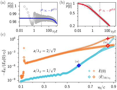
As the gate examples in Sec. II illustrate, individual logic gates can operate fully ballistic, without external energy supply apart from the input fluxons themselves. In Sec. IV the process margins of the gates will be specified based on a velocity ( energy) retention after the gate, although a less stringent criterium may be practical. Even for Nb technology this may allow a ballistic gate with an energy cost on the order , see below. However, a logic architecture consisting of many individual gates needs to include clocking structures to synchronize fluxons. For example, in simulations of a NSWAP gate we find that the two input fluxons of equal velocity must be spaced by less than for proper gate operation. In another work WusOsb2018 we present ‘store-and-launch’ gates which can stop moving fluxons, store the bits as static flux states, and from these later relaunch fluxons in a synchronized way. In the process of stopping a fluxon, it may conserve the fluxon’s potential energy, which makes up of the total fluxon energy (for ). In contrast, conventional SFQ logic gates dissipate several units of bit energy, , per gate HerrETAL2011 ; Tolpygo2016 . We may compare the fluxon’s kinetic energy , which is lost when stopping the fluxon and thus forms an upper boundary for the energy loss in a ballistic gate, with the thermal energy : Demanding that the thermal excitation of plasma waves in the LJJ should be suppressed, we require that , where is the minimum energy of the LJJ plasma spectrum, with and . Thus we see that should exceed , and we can therefore estimate that the (kinetic) energy loss of a fluxon in a stop-and-launch gate may be of the order or larger than . For some realistic designs of the discrete LJJ made with Al (Nb) and for a target temperature of (), the factor may be on the order , thus resulting in a energy loss of .
III Collective Coordinate Model
In this section we describe more details of the collective coordinate (CC) approach leading to Eq. (10), and employ it to explain elastic scattering phenomena in the circuit interfaces.
III.1 Reduced (collective) equations of motion
Starting point of the analysis is the ansatz, Eq. (5), for the fields in the left and right half of the circuit shown in Fig. 1(a), each consisting of a superposition of a fluxon and mirror antifluxon. This ansatz is consistent with the initial-state phases far away from the interface, namely and for a fluxon incident from the left. As found above, Eq. (5) can be used to approximate in the numerically simulated elastic scattering phenomena, e.g. for Figs. 2 and 3. In these fits are independent fit parameters for each time while parameters and were fixed to correspond to the initial fluxon. According to Eq. (5), the symmetry point corresponds to an equilibrium field . Localized excitations around this state are described with , some of which are sketched in the insets of Fig. 7(b1), in particular even-parity excitations with and odd-parity excitations with (labeled as e and o in the insets). A full set of asymptotic scattering states are parametrized by Eq. (5) as illustrated in the insets of Fig. 7(a1): The fluxon in the left LJJ itself is represented by , . Its reflection as an antifluxon is described by , . The forward scattering into fluxon and antifluxon are described with and , respectively, with .
The following paragraphs summarize results of the CC derivation given in App. B.1. The scattering phenomena discussed here occur in a regime of small interface inductance, . In this limit the interface equations of motion allow the approximation . Using this approximation and the ansatz, Eq. (5), the Lagrangian, Eq. (II.1), can be written in a dimensionless form, , as
| (12) |
with the dimensionless particle potential ,
| (13) |
The coordinate-dependent, dimensionless particle masses are
| (14) |
, where are the LJJ contributions to the mass, given in Eq. (33). The interface factor
| (15) |
characterizes the interface contribution to the masses, as well as the coupling mass,
| (16) |
The potential has constituents , , and , which are defined in Eqs. (32), (43), and (B.1), and are illustrated in Fig. 12(a-c). Recall that the LJJ-potential and the interface contribution have even parity under the transformations , for , while the interface contribution has no parity symmetry. All constituents of are symmetric under the left-right exchange , as expected.
The Lagrangian, Eq. (12), generates the coupled equations of motion for
| (17) |
which determine the accelerations by the mass-normalized force . The separate contributions to this force from the potential and from the mass gradients are (cf. Eq. (10))
| (18) | |||||
| (21) |
The mass matrix is composed of the dimensionless elements and () given above.
III.2 General elastic reflection and transmission
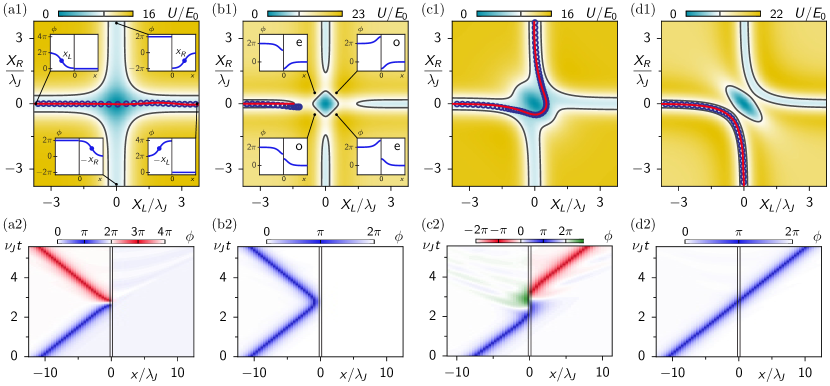
The composite potential is illustrated in Fig. 7(a1) for and , such that both and do not contribute. The potential forms four scattering valleys for the asymptotically free fluxons either left or right of the interface (see insets), which are connected by a central potential well at . The accessible coordinate space is limited by the initial fluxon energy (gray equipotential line). Fig. 7(a1) also shows the trajectory obtained from integration of Eq. (17) with initial condition , , and , corresponding to the incident fluxon (red line). It is in excellent agreement with the corresponding trajectory obtained from fitting with Eq. (5) (blue markers).
Here the interface capacitances are and , such that the coupling is negligible and the acceleration in Eq. (17) remains small in -direction. The resulting motion from to corresponds to the fluxon being reflected as antifluxon, as shown in Fig. 7(a2). Note that, in accordance with an earlier remark, the left particle is throughout this process found at a real-space position within the left LJJ. This scattering is more general than an open LJJ boundary which also generates antifluxon reflection, as a result of the Neumann boundary condition CostabileETAL1978 . Unlike that open boundary, here non-negligible current flows through the left interface junction. We note that in this parameter regime a current-phase relation is observed for elastic reflection at the interface which relates to a general integrable boundary condition for the SGE GhoZam1994 , but which is outside the scope of the current work.
Keeping but raising relative to the previous case results in a finite prefactor to the interface potential and creates a potential barrier at around the center well as shown in Fig. 7(b1) (compare also to in Fig. 12(b)). In particular, if is larger than , scattering between the valleys is prevented and the incident particle is reflected before entering the central potential well, as shown in Fig. 7(b2). This is similar to the simple case of a fluxon reflection at a shunted end of a LJJ (with the Dirichlet boundary condition VanDuzer ), in that the particle will remain fluxon-like.
We next consider where the contribution of the interface potential breaks the even potential parities, as shown in Fig. 7(c1). The trajectory coming in at is therefore subject to a relatively strong acceleration component by which at first it is deflected towards , before moving into the valley with . Note that here we have additionally set large values of , which modify , and also provide a strong mass-gradient acceleration . Under their combined action the trajectory eventually evolves smoothly into the valley at , corresponding to an antifluxon released into the right LJJ, as shown in Fig. 7(c2). This forms an alternative NOT gate to Fig. 3 (Fig. 4(b)). In this alternative, only differs from the interface parameters of the ID gate in Fig. 2 (Fig. 4(a)), and therefore the altered potential is responsible for turning the ID into a NOT gate. Recall the gates of Fig. 4 differ only by , with negligibly small , and thus does not make use of this parity-breaking effect.
If increases further the odd parity contribution in disconnects the center potential well from the valleys, as shown in Fig. 7(d1). However, the asymptotic valleys of equal-polarity fluxons become simply connected: with and with . The trajectory is confined to a curved valley which corresponds to the direct transmission of the fluxon across the interface, as shown in Fig. 7(d2).
III.3 Two NOT gate types, made from one ID gate
Finally, in Figs. 4(a) and (b) the potential and trajectories are illustrated for the interface parameters underlying the gates of Figs. 2 and 3. Recall that both cases have the same potential because the interface parameters are identical. The trajectories demonstrate how the unconventional fluxon dynamics of these cases can be attributed to competition between potential and mass-gradient accelerations, (yellow arrows) and , which create the total acceleration, (green arrows). Forward scattering of the fluxon requires a deflection of the trajectory, initially at , into one of the valleys at . The gates are based on interfaces with very small , such that the potential has approximately even parities. Therefore, a non-negligible mass coupling in Eq. (17) is required to deviate from . First, while approaching the central potential well, , the trajectory is deflected from by the dominant action of , as shown by the green -arrows which point in a different direction than the yellow -arrows. In this limit, and for initially , we calculate the -component of as
| (22) |
Though exponentially suppressed for , initially dominates compared to the other acceleration components, which scale as and . deflects the incoming trajectory towards . Then, once it enters the central potential well at this small deviation experiences a strong restoring force dominated by .
In Fig. 4(b) (the NOT gate) the initial deflection is larger than in Fig. 4(a) (the ID gate) due to the larger value of . Note that the force arrows in Fig. 4 are scaled logarithmically, such that the initial green acceleration arrow in (b) appears only slightly longer compared to (a), while in fact is a factor larger in (b) according to Eq. (22). The result of larger initial acceleration counteracting the motion in (b) is seen in the lower speed of the particle at , as indicated by the smaller separation of the adjacent markers representing the trajectories at equal time steps. The force balance is designed here to symmetrically reflect the trajectory in the potential well at a point on the symmetry line (the velocity-component along that direction vanishes). The result is a total -counter clockwise rotation into the valley with , as described above.
In Fig. 4(a) the initial deflection of the ID gate is reduced by a factor due to the half value of (see Eq. (22)) relative to Fig. 4(b). The trajectory thus retains larger velocity in -direction when entering the central potential. It is then reflected symmetrically across the symmetry line , related to a -rotation. In this case near the symmetry line and thus the velocity-component perpendicular to this line is also small. This results in slower evolution of the phases compared with the NOT gate, and together with the longer trajectory in the central potential well implies a longer gate time of the ID gate.
In contrast to Fig. 4(a) and (b), where a conversion from ID to NOT gate is achieved by a change of the interface parameter alone, this conversion can also be achieved with a different parameter change — by tuning the interface potentials and through . This was discussed in Sec. III.2, where the increase from to generates the NOT gate of Fig. 7(c2). The corresponding CC potential and trajectory are shown in Fig. 7(c1). In this example, the initial deflection to is enhanced compared to the ID gate (Fig. 4(a)) by the parity-breaking influence of the interface potential (other than the parameters are the same). Furthermore, the trajectory is slowed down at due to a potential barrier introduced by , such that the trajectory is symmetrically reflected already across the symmetry line .
IV Gate optimization and robustness
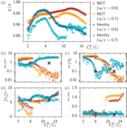
The CC analysis based on Eq. (5) was used to explain the role of interface parameters , , and in the dynamics. For example, in the 1-bit gates a moderately large capacitance is required for the mass coupling to generate a non-negligible initial acceleration in the -direction , as given by Eq. (22). To achieve gate efficiency beyond the CC predictions Monte Carlo optimizations were performed, based on the full simulation with Eq. (II.1), where we vary as a independent variable. For each value of we maximize the final velocity of the fluxon emitted into the right LJJ through random iterations of , and . Fig. 8(a) shows the resulting optimized , obtained with interface parameters presented in Figs. 8(b-e). This is shown for initial velocities and , both for the ID and NOT gates.
For the NOT gate a broad maximum of is found for at , and of for at . At even smaller velocities the maximum is shifted further to higher .
The optimized ID gate has a narrower peak in in the displayed range than the NOT gate, with a maximum at , reaching for and for . The optimum is less dependent on for this gate. Around the peaks in , e.g. for the NOT gate, the interface parameters are relatively constant, or else are negligibly small:
(i) As shown in panel (d), for both gates the optimal is larger than (as well as ). It has the approximate value of for the NOT gate (for ) and for the ID gate (for ). In contrast, if is strongly reduced from these optimal values the resulting larger initial deflection towards can destroy the gate dynamics, as understood from the CC analysis (cf. Eq. (22)). Usually, repeated large-amplitude bounces within the central potential well are then observed. Similar to what happens when is increased (as shown in Fig. 4), when is reduced from the optimized ID gate of Fig. 4(a) with to the initial deflection increases, and as a result the trajectory creates a NOT gate.
(ii) As shown in panels (b) and (c), near the optimization maxima of , both and are small relative to , showing that the short-range interface potentials , are irrelevant for the operations of the optimized gates. Instead these are determined by the balance of mass matrix elements, weighted by and , in the fixed potential . Only away from their respective optima do the gates increasingly appear to rely on the modification of the potential by contribution of and . This is particularly evident in case of the NOT gate, where and at form an elevated plateau, with . For these parameters even yield a sudden increase of by to match the performance of , see panel (a). An example for the dynamics in this regime of large and (interface parameters indicated by large gray marker in Fig. 8(b-e)) is shown in Fig. 7(c). Similarly, for the ID gate away from its optimal , is enhanced, particularly when . This allows to establish a narrower valley in the -direction at (see Fig. 12(b1)), and this compensates for the larger initial due to in Eq. (22). For (below the optimum) much larger values of are observed, and this breaks the even potential parities due to the increased contribution of . This compensates for the smaller initial (arising due to smaller ).
(iii) The Monte Carlo optimization generally yields , as shown in panel (e). This regime is consistent with the assumptions of the CC analysis, which uses . A seemingly large is found in plateaus of the NOT gates at , but this still corresponds to a small expansion parameter , valid in earlier approximations.
The similar parameters for the two gates in Fig. 8 indicate the possibility to convert between the two gate types by adjusting only a single parameter. As examples, we have discussed in Sec. III how the change of either from to , or of from to , can turn a near-optimized ID into a near-optimized NOT gate. The parameters of these three interfaces are indicated in Fig. 8 with the large black and gray markers. As already mentioned, a similar effect can be achieved by decreasing .
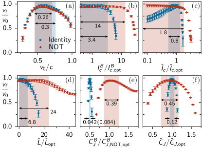
In Fig. 9 we illustrate the gate robustness with respect to variations in the initial conditions and the interface parameters, for the gates of Figs. 2 and 3. Each panel shows the final velocity of the output fluxons under one of these parameter variations. As demonstrated in Fig. 9(a) the final-to-initial velocity ratio as a function of initial velocity is similar for both ID and NOT gates, yielding in the wide interval . For this corresponds to an energy loss , while optimal forward-scattering at the maxima have . The relative insensitivity to the incident velocity is remarkable. Resonant scattering at defects within a LJJ, e.g. local inhomogeneities of or , typically exhibit high sensitivity to velocity variations, as characteristic for chaotic scattering processes FeiKivVaz1992 ; GooHab2007 . We note that our interface cannot directly be compared with a mere LJJ defect: while the latter allows a perturbation treatment within the Sine-Gordon theory, our interface involves an essential additional degree of freedom, , which allows non-perturbative effects.
The robustness against relative variations of one parameter, , with respect to its optimum value is shown in Figs. 9(b-f). The acceptable range of parameter variations seen in these figures is related to the scatter of optimized parameters in Fig. 8, when the gate parameter (large black marker in Fig. 8(b-e)), lies within the scatter range. The value is in the optimized range within the scatter for the values of of both gate types, Fig. 8(d). In this case, greater scatter in the parameter is seen in the NOT gate relative to the ID gate, and thus as expected the NOT gate is less sensitive in the -gate parameter, as seen in Fig. 9(f). In other cases the chosen gate parameters lie outside that scatter range because it is not very sensitive to the parameter, such as in the NOT gate of Fig. 3. The NOT gate is rather insensitive to most parameter variations, including and . In line with previous analysis, is small and therefore it is relatively insensitive for both gate types. For the ID gate the criterion gives a large accessible range of to for parameter . It also gives tolerance ranges for and of and , respectively. Note that the variation of is presented in panel (e) relative to the optimized value of the NOT gate, which is twice that of the ID gate: . From this analysis, the narrowest tolerance range, in capacitance is for the ID gate, but still shows compatibility with current fabrication processes. Further optimization can be performed, and furthermore the tolerance range (margins) can increase by large factors when setting a lower output-velocity criterion.
V 2-bit gate
Now we discuss the interface for the 2-bit gate, Fig. 10(a), which connects two LJJs from each side. It is designed as a generalization of the 1-bit gate interface, in that it is symmetric in propagation direction (left–right), with central junctions in the interface, labeled A,B,C. We also restrict the circuit to the case of vertical symmetry about the B-line, e.g. . We introduce the notation and for the phases across the junctions in the upper and lower LJJs, respectively.
We discuss here the cases of aligned and anti-aligned input fields: and , respectively. For synchronized input fluxons of identical velocity the former corresponds to both having equal polarities, and the latter to opposite polarities. A coupling between fields of upper and lower LJJ can only occur within the interface. The dynamics in the circuit of Fig. 10 cannot be mapped (impedance matched) to dynamics in 1-bit interfaces for arbitrary input fields due to the nonlinear circuit elements. However, as detailed in App. C, it is possible for the above special initial conditions where the dynamics becomes fully equivalent to the independent evolution in 1-bit circuits, such that the initial property remains preserved. For simplicity we argue in the limit of small interface inductances , . Similar to the first-order approximation in the CC analysis of Sec. III.1, this allows us to employ the interface-cell constraints and . Next we schematically summarize the formal analysis provided in App. C for the two initial cases.
Case I, equal polarities:
Here and . The above cell constraints then imply that . This input symmetry together with the device symmetry imply , and thus . The current in the junction with thus vanishes, while the currents in the junctions with and are opposite. Under these conditions, the interface Lagrangian becomes a sum of two independent contributions, and it is therefore clear that and evolve independently. Because of the vertical interface symmetry the initial relations then remains fulfilled for all times . Each of the two independent Lagrangians (Eq. (61)) turns out to be identical to that of an equivalent 1-bit interface, Eq. (B.1), whose center junction equals the A-line junction of the 2-bit interface, (), and whose interface inductance likewise is determined by the A-line inductance . This equivalence is illustrated in Fig. 10(b).
Case II, opposite polarities:
Here and . The cell constraints then imply that . The currents in the junctions with and are equal and their sum is compensated by the current in the B-line. Again, the interface Lagrangian becomes a sum of two independent contributions, Eq. (62), and each of them is identical to that of an equivalent 1-bit interface, compare Eq. (B.2). This equivalence is shown in the schematics of Fig. 10(c). However, compared with the 1-bit interface discussed in the previous case, this one has center junctions both in the A- and the B-line (cf. Fig. 13). In this equivalent 1-bit interface the A-line junction is identical to the original A-line junction of the 2-bit interface, with (). In contrast, the B-line junction has only half of the original capacitance and critical current (,). As a result its junction phase is identical to that in the 2-bit interface, while it carries only half of the current, . The sum of inductances in the equivalent 1-bit interface equals the sum of the 2-bit interface. Furthermore, if the equivalent 1-bit interface itself has vertical symmetry, i.e. if and if the critical currents are negligible, then in the equivalent 1-bit interface with 2 center junctions. The dynamics becomes approximately equivalent to that in a 1-bit interface with only one interface junction, which thus has the equivalent serial capacitance , as shown in Fig. 10(d). See App. B.2 for a detailed discussion including CC analysis of the new 1-bit interface. The CC analysis can also be extended to model other 2-bit gates, if asymmetry prevents a mapping to the two dynamically decoupled 1-bit gates.
In summary, these mappings to 1-bit circuits imply that synchronized fluxons in 2-bit circuits can be made to undergo the forward scattering of 1-bit gates. Moreover, as the mappings are different for equal and opposite polarities of the input fluxons, a 2-bit gate can be designed which deterministically carries out the NOT or ID processes as a controlled gate. An example for this is the controlled NOT SWAP (NSWAP) gate, described above and in Fig. 5 for a 2-bit circuit (with interface parameters , , , , , , and ). For equal polarity fluxons, the equivalent 1-bit interface has, according to the mapping of Fig. 10(b), the inductance and capacitances and , while the critical current of the interface junction is negligible, . Comparing this to the 1-bit gate-optimization curves in Fig. 8 (with line-index instead of ) it is clear that these parameters support a NOT gate, individually executed on both input fluxons. Thus, the input bit-state pairs (0,0) and (1,1) are transformed to output state pairs (1,1) and (0,0), respectively. For opposite polarity fluxons the equivalent 1-bit interface has according to the mapping of Fig. 10(c) a B-junction with capacitance , while all other interface capacitances are invariant, and . When we simulate the fluxon dynamics for this equivalent interface, using the interface Lagrangian for two center junctions, Eq. (B.2) instead of Eq. (B.1) for one center junctions, we observe forward scattering without polarity inversion, similar to Fig. 2. Because this 1-bit interface has approximate vertical symmetry, and negligible , we can further compare it with an (approximately) equivalent 1-bit interface with only one center junction of serial capacitance , as illustrated in Fig. 10(d). Again, from Fig. 8 it is clear that this interface supports an ID gate. For the 1-bit interface this means that the synchronized fluxons here both perform an ID gate, such that input state pairs (0,1) and (1,0) are preserved. The combination of the two input cases creates a NSWAP gate, a gate that depends on the strong interaction of the input fields.
VI Summary and conclusion
We have proposed Reversible Fluxon Logic (RFL) as new reversible logic gate circuits. The bit states are represented by the fluxon and antifluxon state in a long Josephson junction (LJJ) which have opposite topological charge (flux polarity). The RFL gates are built from LJJ segments and a circuit interface between them. The key physical feature of the gates is the resonant nonlinear dynamics induced by the incoming fluxon at the interface. We find through numerical circuit simulations that the fluxon is converted at the interface to and then from a localized oscillation mode, thus realizing a forward scattering of the fluxon from one LJJ to the other. Both the moving fluxon and the localized interface mode have a finite width on the order of the Josephson penetration length , and this facilitates the resonant conversion between these two excitation types. This mechanism therefore distinguishes RFL gates from lumped-element circuits used in SFQ-based (reversible) logic.
Importantly, in the process of forward-scattering at the interface the fluxons can undergo conditional changes of their polarity. This effect provides the means of bit-switching in the RFL gates. The bit-switching is characterized by a -change of a central JJ in the gate interface (see Fig. 1), contrasting the -switching of strongly damped JJs in SFQ digital logic. The dynamics in the RFL gate circuits is powered only by the inertia of incident fluxons, which distinguishes them from previous reversible digital circuits which use power from an adiabatic clock for dynamics. At the same time, while being a ballistic-type of reversible logic, RFL also differs from the classic billiard ball model in that the digital state is not encoded in the particle paths but their topological charge (flux polarity). Contrary to the billiard ball scattering-based gates in 2D, no path correction is therefore needed in RFL gates since given 1D paths are defined by the LJJs for the result.
As shown in Fig. 9, the scattering process at the interface depends on the circuit parameters and (weakly) on the input velocity of the fluxons. RFL gates are defined with those interface parameters which enable the desired scattering type for fluxons at a moderately high input velocity (e.g. ), with a high energy retention of the output fluxons.
The fundamental building blocks of the logic are the 1-bit gate circuits which we design with large shunt capacitances of the three interface JJs (Fig. 1). These capacitances absorb and later release a large fraction of the incoming fluxon’s energy. This process is aided by the evanescent field that is excited around the interface over the Josephson penetration length . Depending on the interface parameters, the new fluxon has inverted or unchanged polarity, and the two circuits therefore define the NOT and Identity (ID) gates, respectively. We note that the NOT and ID gate parameters are not unique; a NOT gate may be obtained from an ID gate by modifying the critical current or capacitance in the interface-center JJ. For example, we showed different NOT gates in Figs. 3 and 7 related to the ID gate of Fig. 2.
As there is no external power supply during the gate operation, the energy cost of an RFL gate is given simply by the energy difference between the output and the input fluxons. The fluxon output velocity and energy is calculated for various gate parameters (see Fig. 8). In our simulations with particular gate parameters, the output fluxons recover of the input fluxon energy, which is at a speed .
In a digital architecture consisting of many RFL gates, of course additional structures are required where fluxons are synchronized and brought back to their nominal speed. Even if fluxons are stopped in such components, the entire potential energy of fluxons could be conserved (i.e. their rest mass which is in our study). In later work WusOsb2018 we describe a circuit structure that allows one to store and launch fluxons for synchronization before entering a ballistic gate. The energy for accelerating the stored fluxons in that structure is supplied by a clock fluxon with low energy relative to the data fluxon.
The operation time of the here presented RFL gates is only a few Josephson oscillation periods such that the gates are fast as well as efficient. Compared with this, the gate cycle in adiabatically-powered reversible gates uses many oscillation periods of a JJ for the operation time in order to meet the adiabatic criteria, to conserve most of the digital state energy .
A 2-bit NSWAP gate was studied as a natural extension of the 1-bit gates. It exhibits (see Fig. 5) one of two types of dynamics, depending on whether the input fluxon polarities are the same or different. For all possible input polarities a dynamically equivalent 1-bit gate can be found, i.e. the coupled dynamics of the 2-bit gate is in each case mapped (see Fig. 10) to that of two uncoupled 1-bit gates. The 2-bit NSWAP was also numerically simulated (see Fig. 6) in a proposed experimental test platform (see Fig. 1(e)) which features capacitive coupling to a ground plane and an imperfect fluxon launch. This simulation shows that the gate operation is robust even in the presence of non-optimized stray capacitance and launch-induced plasma waves that perturb the gate dynamics. Simulations of 1-bit gates were made over a range of parameters, and the output velocity shows that gates are compatible with current fabrication uncertainties (see Fig. 9).
To explain the numerically discovered phenomena of fluxon conversion to resonant excitation, followed by fluxon (or antifluxon) creation we developed and analyzed a collective coordinate model. In this model we parametrize the fields in each LJJ as a superposition of fluxon and mirror antifluxon and thus reduce the many-junction dynamics to that of only two coupled coordinates. We solve the resulting reduced system and find quantitative agreement with the solution of the numerical circuit simulation (see Fig. 4). The model describes motion of fluxons and antifluxons in the LJJs as motion in four valleys of a two-dimensional potential which may also be connected to allow scattering between valleys. The energy-conserving scattering process is described not by fluxons, but as particles that change between fluxon and antifluxon types smoothly in time. The influence of kinetic coupling and mass gradients stemming from the interface are essential to the gate dynamics since there is no external modulation of the potential.
Reversible logic is now successfully realized in recent demonstrations of circuits that commonly share an adiabatic drive to steer the dynamics. However, we find that reversible gates are possible with an unrealized type known as ballistic reversible gates. Our collective coordinate model for 1-bit gates describes the gate dynamics in terms of particles moving in a static potential under the influence of mass-gradient forces. We expect future experimental studies of these gates for scientific and technological purposes. We also provided estimates for energy limitations related to timing and launching a fluxon, as low as the order of , when used in a future possible architecture.
This provides an efficiency benefit over irreversible gates by orders of magnitude. Also, the addition of ballistic gates enhances the breadth of reversible digital logic. This may ultimately be useful to speed development in reversible digital logic similar to the way a broad set of superconducting qubit types advanced quantum reversible logic.
Acknowledgments
KDO and WW acknowledge useful discussions with Q. Herr, V. Semenov, F. Gaitan, and R. Ruskov. WW acknowledges support from University Technical Services.
Appendix A Fluxon radiation in a discrete LJJ
The fluxon in an ideal continuous LJJ can move without energy loss, as described by the soliton solution to the sine-Gordon equation. In a discrete LJJ, as described by the Frenkel-Kontorova model BraunKivshar1998 , the discreteness acts as a perturbation to the Sine-Gordon dynamics. This perturbation causes a coupling between the fluxon and the spectrum of linear plasma waves. As a result, a moving fluxon excites plasma waves and loses energy in a resonant process known as Cherenkov radiation BraunKivshar1998 ; UstinovETAL2008 . For small to moderate discreteness, such as the one used in this work, this process is inefficient, whereas at large discreteness the energy loss due to Cherenkov radiation becomes strong PeyKru1984 .
Here we simulate fluxon motion in our discrete LJJ to show different damping regimes. The dissipation rate of the fluxon energy is strongest at ultra-relativistic speeds, , and decreases by many orders of magnitude for moderate values of , see versus in Fig. 11(c). For fixed value of below the ultra-relativistic regime (such as ) the dissipation rate also drops by orders of magnitude when the effective lattice spacing is decreased. For example, in Fig. 11 we compare dissipation rates for our default value, (light blue), with the doubled value, (orange). At a velocity the dissipation rate of the latter is which may not be negligible e.g. on a time scale of some . Compared to that the dissipation rate for the default discreteness is reduced by orders of magnitude, , and is negligible in the context of this study of gate times on the order of .
The dissipation rate presented in Fig. 11 is calculated from the time-dependent fluxon momentum,
| (23) |
where the velocity follows from the fits of the moving fluxon according to Eq. (3) with fit parameters and . As above, we use the characteristic energy of the continuum equation, and the characteristic momentum is . We then fit vs. time with the function
| (24) |
where are independent fit parameters. This equation follows from a momentum-decay rate proportional to a power of the momentum,
| (25) |
We find that this function describes the momentum decay well over a large range of damping rates, as demonstrated in Figs. 11(a,b). For very small damping rates exponential behavior is recovered, , corresponding to momentum-proportional damping from initial momentum .
Finally, we evaluate the energy dissipation rate,
| (26) |
following from the momentum-energy relation and using from the momentum fit, Eq. (24). In Fig. 11(c) we present both the initial dissipation rate from the fit, (plus), as well as the dissipation rate averaged over a time (diamonds), for two discretenesses as a function of the initial velocity . At large the initial decay rate is much higher than the time-averaged one, showing that the dissipation changes rapidly during the averaging time. This is shown in panel (c) e.g. at , indicated by the (b)-markers for the discreteness , and the time-dependent momentum for this initial velocity and discreteness is shown in panel (b). The initial momentum decay rate of Eq. (25) is large, at , and creates a large initial dissipation rate . As decays quickly in time, is much smaller in comparison. At lower velocity and higher discreteness the energy loss rate is much lower. For example, at and ((a)-markers in panel (c) with the corresponding time-dependent momentum shown in panel (a), is very small at , and therefore both measures coincide.
The sudden reduction of the dissipation rate observed below for the higher discreteness is related to the resonant emission of plasma waves at specific frequencies PeyKru1984 . Once the fluxon velocity falls below this critical value, an individual solution of the resonance condition becomes inaccessible. As a result, emission into that mode is suppressed.
Appendix B Collective coordinate analysis
B.1 Interface with one center junction (1-JJ)
Here we present the CC analysis leading to Eqs. (12)–(21), for the circuit of Fig. 1(a). We separate the Lagrangian in Eq. (II.1) as
| (27) |
where the contributions of left and right LJJ and of the interface are
| (28) | |||||
| (29) | |||||
Here we have included charging and Josephson energy for extra junctions with phases and to the LJJs in Eqs. (28) and (29). To correct for this, the same charging energy and Josephson energy are subtracted in Eq. (B.1) for the interface. This allows us to replace the LJJ-sums in the continuum limit, , by integrals with boundaries and . Inserting and from Eq. (5) these integrations yield
| (31) | |||
| (32) | |||
| (33) |
with (), and dimensionless potential and masses . is shown in Fig. 12(a).
From Eq. (II.1) (or Eqs. (27)–(B.1)) we obtain the equations of motion for the interface junctions,
| (34) | |||||
| (35) | |||||
| (36) |
where we have introduced . We are interested in the regime of , , , , . This allows us to treat Eqs. (34)–(36) in perturbation expansion, with the small parameter . The leading order contribution has , i.e. , while occurring individually in Eqs. (34)–(36) have finite leading-order contributions. One can then use Eq. (36) to determine the next-to-leading order contribution of , . Inserting this in the remaining Eqs. (34)–(35), we obtain equations of motion for and in leading order. This reduced dynamical system is still described by the Lagrangian Eq. (27), but the interface Lagrangian now takes the form
Inserting and from Eq. (5) into Eq. (B.1), where we approximate and , we calculate the interface contribution to the Lagrangian which then reads
| (39) | |||||
with coordinate-dependent masses
| (40) |
and coupling mass
| (41) | |||
| (42) |
compare Eqs. (12)–(15). The interface contributions to the potential are
| (43) | |||||
and are shown in Figs. 12(b) and (c). The potential is symmetric under the coordinate exchange . The contributions and have even parity under each of the transformations (), while has no parity symmetry.
B.2 Interface with two center junctions (2-JJ)

Here we consider a modified 1-bit interface, shown in Fig. 13. It is similar to that in Fig. 1(a), but has a center junction in the A-line of the interface as well as in the B-line. The phase difference over this junction provides an additional degree of freedom, and instead of Eq. (B.1) the interface Lagrangian becomes
| (45) | |||
where are the interface inductances. For brevity we refer to the interface of Fig. 13 as the 2-JJ interface, and to that of Fig. 1(a) as the 1-JJ interface.
Approximate equivalence to 1-JJ interface:
For simplicity we also only discuss the case of vertical symmetry, with and . Under this condition Eq. (B.2) generates the equation of motion
| (46) |
for the phase average
| (47) |
In our simulations the interface initially has . From Eq. (46) it follows that is a fixed point of the dynamics, such that we may set in Eq. (B.2), which then becomes
| (48) | |||
To compare this expression with the Lagrangian of the 1-JJ interface, Eq. (B.1), we first ignore the Josephson potentials. The 2-JJ interface with two (identical) center junctions and values then maps exactly to the equivalent 1-JJ interface and values . Further analyzing the Josephson potentials to quadratic order in the phases we find that the critical current in the 2-JJ interface corresponds to a critical current in the equivalent 1-JJ interface. That means that the scattering at the (approximately) equivalent 1-JJ and 2-JJ interfaces is very similar, provided that either remains small, or the critical currents are small, .
CC analysis:
Now we perform the CC analysis for the 2-JJ interface. To this end we go back to Eq. (B.2), where we again assume vertical symmetry of the interface, but allow for finite . Once again we restrict ourselves to the perturbative case of small interface inductance, . To leading order we obtain the constraint for the interface cell such that and can be expressed through and . With these replacements Eq. (B.2) reads
| (49) | |||
From Eq. (27) together with (B.2) the CC Lagrangian is derived (similar to Sec. B.1),
| (50) | |||
| (51) | |||
| (52) | |||
| (53) | |||
| (54) |
with , , and identical to expressions for the 1-JJ interface (Eqs. (32), (43), (33), and (42)). The -proportional contribution to the interface potential is
and is shown in Fig. 12(d). It differs qualitatively from the for the 1-JJ interface, which is given in Eq. (B.1) and Fig. 12(c).
The form of the reduced dynamical system for remains invariant, Eqs. (17)–(21), but here an additional equation of motion exists for ,
| (56) |
Again, starting from the fixed point, , the CC dynamics can be compared with that of the 1-JJ interface. To this end we substitute parameters as above for the (approximately) equivalent 1-JJ interface. With this substitution most CC quantities become equal to those in Eqs. (39)–(43). One exceptions is the different form of the interface potential , as mentioned above. Another exception is the prefactor of the interface potential . While in the 1-JJ interface has a weighting , Eq. (39), no equivalent weighting appears in Eq. (51). In this study we focus on the case where these differences in the potential are negligible, and the fluxon scattering at the (approximately) equivalent 1- and 2-JJ interface are therefore very similar.
Appendix C Mapping 2-bit gate to 1-bit gates
Here we discuss the Lagrangian for the interface which connects two LJJs from each side, Fig. 10(a). The interface is assumed to be both left–right and vertically symmetric. Using the notation and for the phases across the upper and lower LJJs, respectively, the interface Lagrangian is,
| (57) |
(). Without DC bias from the left to the right of the gate, the currents in the interface lines fulfill , and
| (58) | |||
| (59) |
Similar to the 1-bit interfaces we consider the limit of small interface inductances , which here results in the interface-cell constraints and . The 3rd line in Eq. (C) then becomes negligible.
We discuss the cases of initially equivalent fields in the upper and lower LJJ, . Coupling between and occurs only within the interface. We start with the assumption that or remains fulfilled throughout the evolution. This will be confirmed below by the effective decoupling of the upper and lower interface cell imposed by the symmetry.
Case I, :
The symmetry together with the above cell constraints give . The current on the B-line cancels, . For symmetry reasons, , and thus . Therefore the interface Lagrangian, Eq. (C), is a sum of two independent contributions,
| (60) |
with
| (61) |
and given by the same expression but with the substitutions , and . Since there is no coupling term, and effectively evolve independently. Because of vertical symmetry of the interface the initial relation remains fulfilled for all times, i.e. the fields remain synchronized. Each of the Lagrangians is identical to that of an equivalent 1-bit interface with one center junction, Eq. (B.1), which has characteristic values (), as indicated in Fig. 10(b). Note that the equivalence to the 1-bit interface holds also for finite interface inductances , which we have neglected here for simplicity. The inductance of the equivalent 1-bit interface is then given by .
Case II, :
Here the cell constraints imply that . Again, Eq. (C) is a sum of two independent contributions, with
| (62) | |||
where . The same expression defines , but with the substitutions , and . Each is identical to the Lagrangian of an equivalent 1-bit interface with two center junctions, Eq. (B.2), as indicated in Fig. 10(c). The equivalent center junctions have characteristic values and , respectively. Also the sum of interface inductances in the equivalent 1-bit 2-JJ interface, , equals from the 2-bit interface.
If this equivalent 1-bit 2-JJ interface, moreover, has vertical symmetry, i.e. if , then we can approximately map further to a 1-bit 1-JJ interface, as discussed in App. B.2. This approximately equivalent interface has center-junction values and center inductance of .
References
- (1) International Roadmap for Devices and Systems (2017), https://irds.ieee.org/roadmap-2017, accessed in January 2018.
- (2) T.N. Theis and H.-S.P. Wong, Comput. Sci. Eng. 19, 41 (2017).
- (3) K.K. Likharev and V.K. Semenov: IEEE Trans. Appl. Supercond. 1, 3 (1991).
- (4) Q.P. Herr, A.Y. Herr, O.T. Oberg, and A.G. Ioannidis, J. Appl. Phys. 109, 103903 (2011).
- (5) Private Communications with Anna Herr (2017).
- (6) D.S. Holmes, A.L. Ripple, and M.A. Manheimer, IEEE Trans. Appl. Supercond. 23, 1701610 (2013).
- (7) C.H. Bennett, IBM Journal of Research and Development 17, 525 (1973).
- (8) K.K. Likharev, Int. J. Theor. Phys. 21, 311 (1982).
- (9) J. Ren and V.K. Semenov, IEEE Trans. Appl. Supercond. 21, 780 (2011).
- (10) N. Takeuchi, Y. Yamanashi, and N. Yoshikawa, Sci. Rep. 4, 6354 (2014).
- (11) N. Takeuchi, Y. Yamanashi, and N. Yoshikawa: Phys. Rev. Applied 4, 034007 (2015).
- (12) E. Fredkin and T. Toffoli, Int. J. Theor. Phys. 21, 219 (1982).
- (13) M.N. Islam and C.E. Soccolich, Opt. Lett. 16, 1490 (1991).
- (14) J. Scheuer and M. Orenstein, J. Opt. Soc. Am. B 22, 1260 (2005).
- (15) P.D. Drummond and W. Man, Opt. Commun. 105, 99 (1994).
- (16) D.W. McLaughlin and A.C. Scott, Phys. Rev. A 18, 1652 (1978).
- (17) Z. Fei, Y.S. Kivshar and L. Vázquez, Phys. Rev. A 45, 6019 (1992).
- (18) R.H. Goodman and R. Haberman, Phys. Rev. Lett. 98, 104103 (2007).
- (19) D.V. Averin, K. Rabenstein, and V.K. Semenov, Phys. Rev. B 73, 094504 (2006).
- (20) K.G. Fedorov, A.V. Shcherbakova, M.J. Wolf, D. Beckmann, and A.V. Ustinov, Phys. Rev. Lett. 112, 160502 (2014).
- (21) A. Fedorov, A. Shnirman, G. Schön, and A. Kidiyarova-Shevchenko, Phys. Rev. B 75, 224504 (2007).
- (22) I.I. Soloviev, N.V. Klenov, A.L. Pankratov, L.S. Revin, E. Il’ichev, and L.S. Kuzmin, Phys. Rev. B 92, 014516 (2015).
- (23) K.D. Osborn and W. Wustmann, in Reversible Computation. RC 2018. Lecture Notes in Computer Science 11106, 189 (Springer, Cham, 2018).
- (24) T. Dauxois and M. Peyrard, Physics of Solitons, (Cambridge University Press, Cambridge, 2006).
- (25) A.C. Newell, Solitons in Mathematics and Physics, (Society for Industrial and Applied Mathematics, Philadelphia, 1985).
- (26) O.M. Braun and Y.S. Kivshar, Phys. Rep. 306, 1 (1998).
- (27) J. Pfeiffer, A.A. Abdumalikov, Jr., M. Schuster, and A.V. Ustinov, Phys. Rev. B 77, 024511 (2008).
- (28) M. Peyrard and M.D. Kruskal, Physica D: Nonlinear Phenomena 14, 88 (1984).
- (29) A. Barone and G. Paternò, Physics and Applications of the Josephson Effect, (Wiley, New York, 1982).
- (30) S.K. Tolpygo, Low Temperature Physics 42, 361 (2016).
- (31) G. Costabile, R.D. Parmentier, B. Savo, D.W. McLaughlin, and A.C. Scott Appl. Phys. Lett. 32, 587 (1978).
- (32) S. Ghoshal and A. Zamolodchikov, Int. J. Mod. Phys. A 9, 3841 (1994).
- (33) T. Van Duzer and C.W. Turner, Principles of Superconductive Devices and Circuits, (Prentice Hall, Upper Saddle River, 1999).