Enhanced photon extraction from a nanowire quantum dot using a bottom-up photonic shell
Abstract
Semiconductor nanowires offer the possibility to grow high quality quantum dot heterostructures, and in particular CdSe quantum dots inserted in ZnSe nanowires have demonstrated the ability to emit single photons up to room temperature. In this letter, we demonstrate a bottom-up approach to fabricate a photonic fiber-like structure around such nanowire quantum dots by depositing an oxide shell using atomic layer deposition. Simulations suggest that the intensity collected in our NA=0.6 microscope objective can be increased by a factor 7 with respect to the bare nanowire case. Combining micro-photoluminescence, decay time measurements and numerical simulations, we obtain a 4-fold increase in the collected photoluminescence from the quantum dot. We show that this improvement is due to an increase of the quantum dot emission rate and a redirection of the emitted light. Our ex-situ fabrication technique allows a precise and reproducible fabrication on a large scale. Its improved extraction efficiency is compared to state of the art top-down devices.
I Introduction
Controlling and enhancing the spontaneous emission of quantum emitters is one of the current key issues in the field of nanophotonics. Semiconductor quantum dots (QDs) are considered as promising and efficient single-photon emitters for quantum optics applications. Michler et al. (2000); Santori et al. (2001, 2002); Zrenner et al. (2002); Akopian et al. (2006); Shields (2007) Over the past few years, several approaches have been pursued to control their emission properties, from the use of photonic crystals Viasnoff-Schwoob et al. (2005); Lund-Hansen et al. (2008) to top-down photonic wires Claudon et al. (2010); Heinrich et al. (2010); Bleuse et al. (2011) and trumpets.Munsch et al. (2012, 2013) These strategies are based on the early work of PurcellPurcell (1946) which demonstrated that the spontaneous emission of an emitter can be modified by engineering its electromagnetic environment. They rely on a waveguiding approach to increase the coupling between a well-defined propagating optical mode and the QD while simultaneously reducing the coupling between the QD and background radiation modes, offering control of both the optical mode profile and the QD spontaneous emission rate.
In this context, the interest of the dot-in-a-nanowire configuration fabricated using bottom-up methods naturally arises because it provides a simple way to ensure the centering of a single quantum emitter in the photonic structure.Reimer et al. (2012); Bulgarini et al. (2012, 2014) The bottom-up fabrication method also avoids heavy processing, like etching the semiconducting material, that is often detrimental to the QDs optical properties. However, the main realizations up to now concern III-V semiconductors, Reimer et al. (2012); Bulgarini et al. (2012, 2014) limiting the operation range to the cryogenic temperature. Tackling this issue, the potential of II-VI materials, in particular CdSe QDs inserted inside ZnSe nanowires (NWs) has been demonstrated in previous studies. They allow for robust high temperature single-photon emission using heteroepitaxial Tribu et al. (2008) or homoepitaxial Bounouar et al. (2012) nanowire growth. Contrary to all the aforementioned systems where the photonic wire structure has a diameter comparable to the wavelength of the guided light which allows for highly efficient coupling to the HE11 modeNowicki-Bringuier et al. (2008), the diameter of the II-VI NW embedding the QD () is much smaller than the wavelength of the emitted light (). It leads to light emission predominantly into non-guided radiation modes and a low collection efficiency. An additional fabrication effort has thus to be made to ensure an efficient coupling to the collection optics.
In a previous reportCremel et al. (2014) we have theoretically investigated the potential of using an oxide shell deposition on a bare ZnSe NW to form a thick photonic wire structure. In this article, we experimentally demonstrate the use of atomic layer deposition (ALD) to fabricate a conformal aluminum oxide (Al2O3) shell around ZnSe NWs containing a single CdSe QD. We show that the oxide shell drastically enhances the light intensity emitted by the QD, and we use time-resolved microphotoluminescence to systematically study the effect of the shell thickness on the nanowire quantum dot (NWQD) emission rate. Our results are compared to numerical simulations accounting for the real NW geometry, evidencing the different physical mechanisms leading to the enhancement of the spontaneous emission from the QD and to the improved light collection from the emitting structure.
II Principles of operation
To illustrate the effect of the NW and its surrounding medium on the QD emission rate, let us consider a QD placed inside an infinitely long cylinder as illustrated in Fig. 1(a) radiating a field at a wavelength . The cylinder is made of a dielectric material (refractive index ) and has a diameter . We first consider a dipole orientation perpendicular to the NW axis in order to use the NW as a propagation medium for the emitted light. In the limit where , the dielectric screening effectBleuse et al. (2011) reduces the spontaneous emission rate by a factor:
| (1) |
where is the radiative emission rate in the bulk material of index .Claudon et al. (2013) For a ZnSe cylinder ( = 2.68 at =), the screening factor is 1/45. If the NW is surrounded by a shell of refractive index instead of vacuum, equation 1 remains valid by replacing with the index contrast . For an \ceAl2O3 surrounding medium (1.77), the screening factor becomes 1/4.1, resulting in an order of magnitude larger radiative rate.
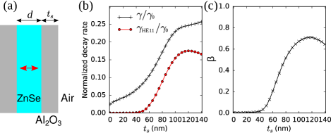
In addition to changing the dielectric screening, the \ceAl2O3 shell also influences the guiding of light along the NW. We have computed the total emission rate and the emission rate into the fundamental HE11 waveguide mode from a radial dipole as function of the shell thickness [see Fig. 1(a)] using a semi-analytical approachYariv (1997) combined with an efficient non-uniform discretization scheme in k space.Häyrynen et al. (2016) The results are plotted in Figure 1(b). We observe that the shell thickness of not only leads to an increased total emission rate, it also allows for confinement of the fundamental HE11 mode to the core-shell NW leading to a preferential coupling of the emitted light to this mode. Figure 1(c) presents the spontaneous emission factor representing the fraction of emitted light coupled to the HE11 mode. We observe indeed that up to 71% of the emitted light is coupled to this mode for =. The dipole thus becomes coupled to the equivalent of a monomode photonic wireClaudon et al. (2010); Heinrich et al. (2010); Bleuse et al. (2011); Reimer et al. (2012); Bulgarini et al. (2012, 2014) paving the way to the control of its far-field radiation pattern.
III Sample fabrication
Our emitters are CdSe QDs embedded inside a ZnSe NW with a thin, epitaxial passivation Zn0.83Mg0.17Se shell grown around the NW. They are grown by molecular beam epitaxy on a GaAs(111)B substrate. A ZnSe buffer layer is first grown on the GaAs substrate after which a thin layer of Au (less than one monolayer thick) is evaporated on the sample surface and dewetted at to form small ( diameter) Au droplets that serve as a catalyst for the NW growth. The substrate temperature is then set at and a flux of Zn and Se atoms with an excess of Se is used, inducing preferential growth of vertical ZnSe NWs. The NWs are in wurtzite phase and their diameter is the same as the droplet ( diameter). The thickness of the initial Au layer is chosen to ensure a low NW density ( 1 NW per ). After the growth of a high NW, the atom fluxes are stopped to allow the evacuation of residual Se atoms inside the droplet. Then, the QD is grown under a flux of Cd and Se atoms for . The fluxes are interrupted again before the ZnSe growth is resumed, resulting in an expected QD height of 2- inserted in a high NW. Finally, an epitaxial Zn0.83Mg0.17Se shell ( thick) is grown around the NW at . A scanning electron microscope (SEM) image of such a CdSe/ZnSe/ZnMgSe core/shell NWQD system is presented in Figure 2(a). The flag-shape termination of the NW is formed during the growth of the ZnMgSe shell. It is present in some NWs.
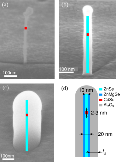
The higher bandgap of Zn0.83Mg0.17Se shell prevents the charge carriers to recombine non-radiatively on the ZnSe NW sidewall and hence improves the quantum yield of the CdSe emitter. In principle, it could directly be used to grow a photonic wire of diameter around the NWQD. However, during the epitaxial shell growth two phenomena are competing: the radial growth of the shell around the wurtzite NWs, and the vertical growth of a 2D Zn0.83Mg0.17Se layer on the sample surface. The radial shell growth rate is very low because the growth of ZnSe on WZ surfaces is not favourable. Because of this low shell growth rate, a trade-off has to be found to avoid burying the NWs in a Zn0.83Mg0.17Se matrix. As a result, only thin epitaxial shells can be fabricated.
The complexity of creating a thick epitaxial shell is one of the reasons why we fabricate the photonic structure by depositing an oxide shell around the NW using ALD. Another reason is that, since this process step can be done separately from the NW growth process, it allows to tune ex situ the shell parameters after a first optical characterization of the QD. Indeed, due to its slow deposition rate, the ALD process allows to precisely control the deposited thickness, which can also be finally verified using scanning electron microscopy. We have tested several oxide materials, and selected Al2O3 because it produced very smooth and conformal, amorphous shells. Figure 2(b) and (c) show two SEM images of the resulting oxide shell deposition ( and ), and the complete structure is sketched in Fig. 2(d). We note that the conformal deposition allows to end the NW+shell structure by an almost perfect half-sphere as can be seen in Fig. 2(b,c). ALD also buries the Au droplet under the shell. The latter might interact with the field emitted by the QD through its localized plasmon resonance. Considering its small diameter it will essentially absorb the incoming field. Moreover the guided HE11 mode profile presents a minimum on the NW axis. This is why we neglect the droplet influence in the following.
IV Experimental results
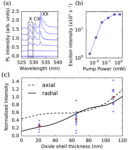
A sample from a single epitaxial growth process is cut in pieces, and photonic structures with different oxide shell thicknesses are fabricated. Taking advantage of the low NW density, individual structures are optically characterized directly on the growth substrate. The samples are mounted on the cold finger of a He-flux cryostat and cooled down to . Individual photonic structures are probed using confocal microphotoluminescence (µPL). They are excitated by a supercontinuum pulsed laser (Fianium WhiteLase, pulse duration, repetiton rate ) and a spectrometer selecting a bandwidth centered around . This excitation energy, below the ZnSe gap, allows us to induce crossed transitions between delocalized states in the NW 1D continuum and a discrete confined 0D state in the NWQD band structureVasanelli et al. (2002). In this configuration, the NW axis is aligned with the optical axis and emission from the QD is collected by a objective. A typical NWQD spectrum is presented in Figure 3(a) as a function of the pump laser power. Three lines can be identified and are attributed to the exciton (X), the charged exciton (CX) and the bi-exciton (XX) respectively. The total emission intensity of the X line as a function of the pump power is reported in Figure 3(b). It shows a linear increase at low pumping power, and a constant plateau at high pumping powers corresponding to the saturation of the exciton level.111We note that single-photon emission is preserved if one integrates both the signal from the X and CX lines.Sallen2009 Under pulsed excitation, we note that changing the shell thickness might modify the laser power in the NW and the excitation probability of the QD. Hence if affects the slope at low power in Fig. 3(b). It has however no effect on the saturation plateau which only depends on the QD emission rate and light collection efficiency. This allows us to compare statistical sets of nanostructures with different oxide shell thicknesses. The total integrated emission at saturation as a function of the oxide shell thickness is reported in blue markers for each NWQD in Figure 3(c). The values have been normalized to the average intensity at . For NWs without an oxide shell, the luminescence intensity is very low and we were never able to reach the saturation regime, this is why we do not report the corresponding points in Fig. 3(c). For each shell thickness, we observe a large spread in exciton saturation intensity. However, we note a general trend of increasing saturation intensity with increasing shell thickness, as demonstrated by the red markers which show the position of the average intensity of our measurements for each shell thickness. On average, the deposition of a thick shell results in the experiments in an almost 4-fold enhancement of the collected intensity with respect to the thick shell case. The semi-analytical calculations show that this enhancement is 10-fold when we compare to a NW without oxide shell.
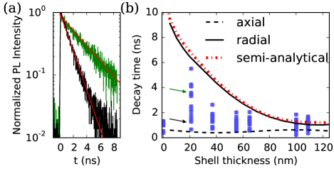
The observed increase in intensity at saturation corresponds to the combination of improved collection efficiency through light redirection from the structure and enhancement of the spontaneous emission rate. In the latter case, a modification of the QD dynamics is expected to be detected by measuring the exciton decay rate. Time-resolved measurements were carried out using a low pump power as compared to the exciton saturation power to avoid any repopulation of the X level. The measured decay transients are thus monoexponential. The fitted decay constant is the total exciton decay time . The experiment was carried out in another setup on a different set of photonic structures compared to the one of figure 3(c). The same excitation laser was used, the QD fluorescence was spectrally filtered in a spectrometer (500gr/mm grating) and integrated on an avalanche photodiode in a photon correlation setup, using the exit slit of the spectrometer as a spectral bandpass filter. The results of these measurements, presented in Figure 4 show also a great dispersion in decay time. One observes however that longer lifetimes are observed for smaller shell thickness (up to ). Increasing the shell thickness leads to an overall decrease in the measured exciton lifetime, hence an enhancement of the exciton decay rate in agreement with the results of the numerical simulations. For systems without an oxide shell, only a few NWQDs give a large enough signal to be properly measured. They yield a much smaller dispersion of short decay times.
V Discussion and comparison to numerical simulations
V.1 Dispersion of the results
For each oxide shell thickness, the large variations of the experimental results in both Figs. 3(c) and 4 have several possible origins. First, the presence of non-radiative recombination channels can reduce the intensity at saturation and change the decay time. The non-radiative recombination rate can vary from QD to QD because of fabrication inhomogeneities, leading to a spread in the measured values.Stepanov et al. (2015) Second, variations in the QD aspect ratio and piezoelectric fields induced internal strain applied by both the ZnSe core and the Zn0.83Mg0.17Se shell lead to different overlap of electron and hole wavefunctions and hence different exciton oscillator strengths. Finally, considering the QD aspect ratio and internal strain, we expect a heavy-hole exciton type for our QDs.Eshelby (1957, 1959); Zieliński (2013); Ferrand and Cibert (2014) Heavy-hole exciton recombination results in a mixture of circularly polarized emission, composed of two degenerate out-of-phase radial dipoles. However, strain and confinement effects might lead to valence band mixing between light hole and heavy hole levels,Karlsson et al. (2006); Tonin et al. (2012); Jeannin et al. (2017) resulting in an emission composed of a mixture between axial and radial dipoles and hence to a spread in total emitted intensity, as we discuss later. Additional measurements on NWQDs grown in similar conditions and mechanically dispersed on a substrate (i.e. lying horizontally on it) revealed that one NWQD out of 6 emit light polarized along the NW axis, while others emit light polarized perpendicularly to the NW axis, evidencing the presence of both kinds of dipoles. Due to the Zn0.83Mg0.17Se shell and low temperature of observation, we expect that non-radiative effects play a minor role. The epitaxial shell prevents non-radiative decay channels owing to surface traps. Additional measurements as a function of temperature show that both the emission intensity and the decay time do not change significantly up to 150- (not presented here). This indicates that the non-radiative effects are not dominating at low temperature, as in the present experiment. While we cannot yet completely rule out the contribution of non-radiative effects, we think that the major effect to explain the dispersion of the results comes from variations in valence band mixing and oscillator strength due to the local environment of the QD. Finally let us stress that the shortest decay times (1-) we measure remain longer than the decay time of CdSe self-assembled QD embedded in bulk ZnSe (<)Bacher et al. (1999). The reduction of the dielectric screening effect is a main effect we evidence.
V.2 Collected intensity and radiative lifetime
To better understand the effect of the shell deposition on the NWQD emission, we perform numerical simulations of the photonic structure formed by the full NW + oxide shell geometry [see Fig. 2(d)]. It takes into account the presence of the ZnSe substrate, and the \ceAl2O3 shell and layer deposited on the NWs and substrate. The QD is modeled as an oscillating electric dipole, either in the axial direction (along the NW axis) or in the radial direction (orthogonal to the NW axis). We perform finite-element method simulations (Comsol v4.1) to compute the total field radiated by the dipole.Jeannin et al. (2017) For each shell thickness and dipole orientation, we evaluate the power radiated towards the objective by computing the flux of the Poynting vector over a surface limited by its numerical aperture (NA=0.6) in a region far from the NW where near field can be neglected. The results of these simulations are reported in Figure 3(c) in black lines for an axial (dashed line) or radial (solid line) dipole. The results are normalized to the axial intensity at . Comparing the simulated integrated intensity in the case of a and reveals an enhancement factor less than 2-fold for an axial dipole and almost 4-fold for a radial dipole. The 4-fold enhancement observed in our measurements suggests that on average, the dominant emitting dipole in our structure is radial, in good agreement with the recombination of a heavy hole exciton.
The theoretical limits for the radiative lifetimes is extracted from the numerical simulations by integrating the total power radiated over every direction for the two dipole orientations (radial and axial) . We normalize this value by the same quantity computed for a dipole in bulk \ceZnSe . For a purely radiative system we have Novotny and Hecht (2012), where and are the radiative lifetime for the nanostructure and for bulk \ceZnSe respectively. Radiative times are presented in black lines in Figure 4, where we have chosen in good agreement with previously reported radiative lifetime of CdSe QD in bulk ZnSeFlissikowski et al. (2001). The axial dipole radiates with an almost constant decay time as a function of the oxide shell thickness, while the radial dipole decay time strongly decreases with increasing oxide shell thickness . Additionally, we compare the decay time for the radial dipole computed for the full geometry to the semi-analytical calculations for the infinite NW presented in fig. 1(b) with the same value. The agreement is excellent indicating that interference effects due to reflections from the substrate and from the top hemispherical termination are negligible.
Comparing the trends of the simulations, we can confirm that our emitters bear a strong radial dipole character. The measurements dispersion can be well understood by considering that the real emitters are a mixture of radial and axial dipoles radiating with a characteristic decay time comprised between the simulated lifetimes of the pure radial and axial dipole. We do not observe long decay time for NWQDs without an oxide shell in Fig. 4. For these systems, it is very difficult to find emitters which are bright enough to be detected is because both the laser absorption and the emission rate of a radial dipole are very weak for such small NW diameters. We think that the emitters which have been selected correspond to NWQDs having a large fraction of axial dipole character as they are the brightest ones when no oxide shell is present.
V.3 Radiation pattern
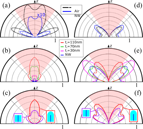
To analyze the mechanisms leading to the increase in collected intensity with increasing shell thickness, we present in Figure 5 several simulated radiation patterns. They are represented as polar plots of the far-field intensity in the top plane, is the angle between the direction of observation and the vertical axis. Simulations are made using respectively a radial dipole [along , Figures 5(a-c)] or an axial dipole [along , Figures 5(d-f)].
Figures 5(a,d) show the effect of the NW structure alone (no oxide shell being present) on such dipoles by comparing it to the case of a free standing dipole in vacuum above the same ZnSe substrate. One can see that the presence of the NW does not affect the shape of radiation diagram, which is essentially determined by the interferences between the directly radiated field and its reflection on the substrate. Most remarkably, in the case of the radial dipole the presence of the NW dramatically reduces the emission intensity through the dielectric screening effect discussed earlier. Simulations show a radiative rate reduction by a factor in agreement with the dielectric screening value predicted by Eq. (1). In contrast, in the case of the axial dipole it can be seen that the presence of the NW only slightly increases the emitted intensity.
Figures 5(b,e) show the computed radiation patterns of the NWQD for increasing oxide shell thickness . In the case of the radial dipole, the shell first reduces the index contrast between the NW and the surrounding medium (cf. Eq. 1), resulting in a strong reduction of the emitter lifetime and thus in an increased total emitted intensity as seen in in Fig. 3(c) and Fig. 4. Note that the the intensity pattern shown in the polar plot must be multiplied by the solid angle if one wants to evaluate the power radiated in the numerical aperture. This is why the intensity for an axial dipole can be larger than for a radial one, as seen in Fig. 3(c). Second, as shown in Figure 1(c), the shell presence ensures preferential emission into the guided HE11 mode for increasing shell thickness. As a consequence a near-Gaussian far-field emission pattern corresponding to the far-field emission profile of the HE11 modeGregersen et al. (2008) is observed for =, contrary to the structures with a smaller oxide shell thickness where one observes the presence of two closely-spaced lobes at small emission angles ( with respect to the -axis). The resulting emission into the 0.6 NA cone is maximum for , where the emission into the HE11 mode is nearly maximum [cf. Fig. 1(b)]. The effect of the oxide shell thickness on the axial dipole is completely different. While the total emitted intensity does not vary much, and hence the emitter lifetime stays constant (as noted in Fig. 4), the light emitted by the axial dipole does not couple to the HE11 mode but is emitted exclusively into radiation modes. Thus the fraction of intensity emitted towards the collection lens increases only slightly as the oxide shell thickness increases [cf. Fig.5(e)]. This intensity increase for the axial dipole also presented in Fig.3(c) is not due to a change in the spontaneous emission rate of the emitter, but rather to a slight redirection of the emitted light.
Finally, Figures 5(c,f )compare the actual hemispherical geometry of the oxide shell termination to the flat end of a simple lateral shell. They show that the presence of the hemisphere is beneficial to the radiation pattern for both kinds of dipole. For the radial dipole, the hemisphere enables a near-adiabatic expansion of the HE11 modeGregersen et al. (2008) leading to a narrowing of the far-field emission pattern and an increased collection by the numerical aperture. The axial dipole benefits less from the hemispherical termination of the photonic structure since no light from this dipole is coupled to the HE11 mode. We also note that half of the emitted light propagates towards the growth substrate and due to the index-matching condition between the NW and the substrate, this light is predominantly lost.
In order to assess the performances of our device we compute the ratio between the power radiated into a 0.6 NA to the one radiated into the top air side hemisphere. This parameter is a good figure of merit for the antenna redirection effect although it cannot be directly related to the overall collection efficiency because of the power lost in the substrate. For our full photonic structure and a radial dipole one has 80% for =. This value reduces to 66% for a flat terminated core-shell photonic wire illustrating the importance of the adiabatic expansion of the HE11 guided mode at the end of the wire. For the dipole in the NW without shell 55%. We have also simulated a structure inspired by state-of-the-art devices fabricated by top-down methods in Ref. Claudon et al. (2010). In this case we simulate a oxide shell photonic wire where the hemispherical termination is replaced by a conical tapper of \ceAl2O3 whose radius progressively decreases from 120 to in . In this case one has 94%, showing that although beneficial our hemispherical termination is not optimal.
VI Conclusion
In summary, we have presented a bottom-up approach to fabricate a dielectric antenna around a QD inserted inside a NW. This method allows for both reproducible and very precise fabrication of the structure on a large ensemble of emitters at once. It is based on the deposition of a thick oxide shell around the NW using atomic layer deposition. Experiments show a 4-fold enhancement of the QD photoluminescence shown in Fig. 3(c) between a and a thick shell. Semi-analytical calculations and numerical simulations of the structure reveal that the oxide shell thickness strongly acts on the radial dipole emission through two main phenomena: the reduction of the dielectric screening, which increases the spontaneous emission rate from the QD, and the redirection of light through a waveguiding effect. Simulations suggest that the collected intensity is multiplied by a factor 7 with respect to the bare NW case. The fabrication process of the photonic shell is very simple and can be applied to QDs emitting single photons up to room temperature. Although not optimal, the resulting structure is a step towards the best nanowire single photon sources operating at low temperatureClaudon et al. (2010). Dielectric screening could be further reduced by growing an oxide shell of higher index matching like \ceTiO2. We note also that in our system a large fraction of the emitted power is radiated in the substrate. This loss channel could be reduced by having a mirror at the bottom of the structure.Friedler et al. (2008); Reimer et al. (2012) Moreover, to fully benefit from the waveguiding approach, a better control on the intrinsic QD properties has to be reached to ensure the presence of radial dipoles, which radiate more efficiently in the experimental collection aperture.
Acknowledgements.
This work was supported by the French National Research Agency under the contract ANR-10-LABX-51-01 and the Danish Research Council for Technology and Production (LOQIT Sapere Aude grant DFF #4005-00370).References
- Michler et al. (2000) P. Michler, A. , Kiraz, C. Becher, W. V. Schoenfeld, P. M. Petroff, L. Zhang, E. Hu, and A. Imamoglu, “A quantum dot single-photon turnstile device,” Science 290, 2282–2285 (2000).
- Santori et al. (2001) Charles Santori, Matthew Pelton, Glenn Solomon, Yseulte Dale, and Yoshihisa Yamamoto, “Triggered single photons from a quantum dot,” Phys. Rev. Lett. 86, 1502 (2001).
- Santori et al. (2002) Charles Santori, David Fattal, Jelena Vučković, Glenn S. Solomon, and Yoshihisa Yamamoto, “Indistinguishable photons from a single-photon device,” Nature 419, 594–597 (2002).
- Zrenner et al. (2002) A. Zrenner, E. Beham, S. Stufler, F. Findeis, M. Bichler, and G. Abstreiter, “Coherent properties of a two-level system based on a quantum-dot photodiode,” Nature 418, 612–614 (2002).
- Akopian et al. (2006) N. Akopian, N. H. Lindner, E. Poem, Y. Berlatzky, J. Avron, D. Gershoni, B. D. Gerardot, and P. M. Petroff, “Entangled photon pairs from semiconductor quantum dots,” Phys. Rev. Lett. 96, 130501 (2006).
- Shields (2007) Andrew J. Shields, “Semiconductor quantum light sources,” Nature Photon. 1, 215 (2007).
- Viasnoff-Schwoob et al. (2005) E. Viasnoff-Schwoob, C. Weisbuch, H. Benisty, S. Olivier, S. Varoutsis, I. Robert-Philip, R. Houdré, and C. J. M. Smith, “Spontaneous emission enhancement of quantum dots in a photonic crystal wire,” Phys. Rev. Lett. 95, 183901 (2005).
- Lund-Hansen et al. (2008) T. Lund-Hansen, S. Stobbe, B. Julsgaard, H. Thyrrestrup, T. Sünner, M. Kamp, A. Forchel, and P. Lodahl, “Experimental realization of highly efficient broadband coupling of single quantum dots to a photonic crystal waveguide,” Phys. Rev. Lett. 101, 113903 (2008).
- Claudon et al. (2010) Julien Claudon, Joël Bleuse, Nitin Singh Malik, Maela Bazin, P ’erine Jaffrennou, Niels Gregersen, Christophe Sauvan, Philippe Lalanne, and Jean-Michel Gérard, “A highly efficient single-photon source based on a quantum dot in a photonic nanowire,” Nature Photon. 4, 174–177 (2010).
- Heinrich et al. (2010) J. Heinrich, A. Huggenberger, T. Heindel, S. Reitzenstein, S. Höfling, L. Worschech, and A. Forchel, “Single photon emission from positioned GaAs/AlGaAs photonic nanowires,” Appl. Phys. Lett. 96, 211117 (2010).
- Bleuse et al. (2011) Joël Bleuse, Julien Claudon, Megan Creasey, Nitin. S. Malik, Jean-Michel Gérard, Ivan Maksymov, Jean-Paul Hugonin, and Philippe Lalanne, “Inhibition, enhancement, and control of spontaneous emission in photonic nanowires,” Phys. Rev. Lett. 106, 103601 (2011).
- Munsch et al. (2012) Mathieu Munsch, Julien Claudon, Joël Bleuse, Nitin S. Malik, Emmanuel Dupuy, Jean-Michel Gérard, Yuntian Chen, Niels Gregersen, and Jesper Mørk, “Linearly polarized, single-mode spontaneous emission in a photonic nanowire,” Phys. Rev. Lett. 108, 077405 (2012).
- Munsch et al. (2013) Mathieu Munsch, Nitin S. Malik, Emmanuel Dupuy, Adrien Delga, Joël Bleuse, Jean-Michel Gérard, Julien Claudon, Niels Gregersen, and Jesper Mørk, “Dielectric gaas antenna ensuring an efficient broadband coupling between an inas quantum dot and a gaussian optical beam,” Phys. Rev. Lett. 110, 177402 (2013).
- Purcell (1946) E.M. Purcell, “Spontaneous emission probabilities at radio frequencies,” in Proceedings of the American Physical Society, Vol. 69 (American Physical Society (APS), 1946) p. 674.
- Reimer et al. (2012) Michael E. Reimer, Gabriele Bulgarini, Nika Akopian, Moïra Hocevar, Maaike Bouwes Bavinck, Marcel A. Verheijen, Erik P.A.M. Bakkers, Leo P. Kouwenhoven, and Val Zwiller, “Bright single-photon sources in bottom-up tailored nanowires,” Nature Comm. 3, 737 (2012).
- Bulgarini et al. (2012) Gabriele Bulgarini, Michael E. Reimer, Tilman Zehender, Moiïra Hocevar, Erik P. A. M. Bakkers, Leo P. Kouwenhoven, and Valery Zwiller, “Spontaneous emission control of single quantum dots in bottom-up nanowire waveguides,” Appl. Phys. Lett. 100, 121106 (2012).
- Bulgarini et al. (2014) G. Bulgarini, M. E. Reimer, M. B. Bavinck, K. D. Jöns, D. Dalacu, P. J. Pool, E. P. Bakkers, and V. Zwiller, “Nanowire waveguide launching single photons in a gaussian mode for ideal fiber coupling,” Nano Lett. 14, 4102–4106 (2014).
- Tribu et al. (2008) Adrien Tribu, Gregory Sallen, Thomas Aichele, Régis André, Jean-Philippe Poizat, Catherine Bougerol, Serge Tatarenko, and Kuntheak Kheng, “A high-temperature single-photon source from nanowire quantum dots,” Nano Lett. 8, 4326–4329 (2008).
- Bounouar et al. (2012) S. Bounouar, M. Elouneg-Jamroz, M. den Hertog, C. Morchutt, E. Bellet-Amalric, R. André, C. Bougerol, Y. Genuist, J.-Ph. Poizat, S. Tatarenko, and K. Kheng, “Ultrafast room temperature single-photon source from nanowire-quantum dots,” Nano Lett. 12, 2977 (2012).
- Nowicki-Bringuier et al. (2008) Y.-R. Nowicki-Bringuier, R. Hahner, J. Claudon, G. Lecamp, P. Lalanne, and J.-M. Gérard, “A novel high-efficiency single-mode single photon source,” Ann. Phys. 32, 151 (2008).
- Cremel et al. (2014) T. Cremel, M. Elouneg-Jamroz, E. Bellet-Amalric, L. Cagnon, S. Tatarenko, and K. Kheng, “Bottom-up approach to control the photon outcoupling of a II-VI quantum dot with a photonic wire,” Phys. Status Solidi C 11, 1263 (2014).
- Claudon et al. (2013) Julien Claudon, Niels Gregersen, Philippe Lalanne, and Jean-Michel Gérard, “Harnessing light with photonic nanowires: Fundamentals and applications to quantum optics,” ChemPhysChem 14, 2393–2402 (2013).
- Yariv (1997) A. Yariv, Optical electronics in modern communications (1997).
- Häyrynen et al. (2016) Teppo Häyrynen, Jakob Rosenkrantz de Lasson, and Niels Gregersen, “Open-geometry Fourier modal method: modeling nanophotonic structures in infinite domains,” J. Opt. Soc. Am. A 33, 1298 (2016).
- Vasanelli et al. (2002) A. Vasanelli, R. Ferreira, and G. Bastard, “Continuous absorption background and decoherence in quantum dots,” Phys. Rev. Lett. 89 (2002), 10.1103/physrevlett.89.216804.
- Note (1) We note that single-photon emission is preserved if one integrates both the signal from the X and CX lines.Sallen2009.
- Stepanov et al. (2015) Petr Stepanov, Adrien Delga, Xiaorun Zang, Joël Bleuse, Emmanuel Dupuy, Emanuel Peinke, Philippe Lalanne, Jean-Michel Gérard, and Julien Claudon, “Quantum dot spontaneous emission control in a ridge waveguide,” Appl. Phys. Lett. 106, 041112 (2015).
- Eshelby (1957) J. D. Eshelby, “The determination of the elastic field of an ellipsoidal inclusion, and related problems,” Proc. R. Soc. A 241, 376–396 (1957).
- Eshelby (1959) J. D. Eshelby, “The elastic field outside an ellipsoidal inclusion,” Proc. R. Soc. A 252, 561–569 (1959).
- Zieliński (2013) M. Zieliński, “Fine structure of light-hole excitons in nanowire quantum dots,” Phys. Rev. B 88, 115424 (2013).
- Ferrand and Cibert (2014) David Ferrand and Joël Cibert, “Strain in crystalline core-shell nanowires,” Eur. Phys. J. Appl. Phys. 67, 30403 (2014).
- Karlsson et al. (2006) K. F. Karlsson, V. Troncale, D. Y. Oberli, A. Malko, E. Pelucchi, A. Rudra, and E. Kapon, “Optical polarization anisotropy and hole states in pyramidal quantum dots,” Appl. Phys. Lett. 89, 251113 (2006).
- Tonin et al. (2012) Catherine Tonin, Richard Hostein, Valia Voliotis, Roger Grousson, Aristide Lemaitre, and Anthony Martinez, “Polarization properties of excitonic qubits in single self-assembled quantum dots,” Phys. Rev. B 85, 155303 (2012).
- Jeannin et al. (2017) Mathieu Jeannin, Alberto Artioli, Pamela Rueda-Fonseca, Edith Bellet-Amalric, Kuntheak Kheng, Régis André, Serge Tatarenko, Joël Cibert, David Ferrand, and Gilles Nogues, “Light-hole exciton in a nanowire quantum dot,” Phys. Rev. B 95 (2017), 10.1103/physrevb.95.035305.
- Bacher et al. (1999) G. Bacher, R. Weigand, J. Seufert, V. D. Kulakovskii, N. A. Gippius, A. Forchel, K. Leonardi, and D. Hommel, “Biexciton versus exciton lifetime in a single semiconductor quantum dot,” Phys. Rev. Lett. 83, 4417–4420 (1999).
- Novotny and Hecht (2012) L. Novotny and B. Hecht, Principles of Nano-Optics, 2nd ed. (2012).
- Flissikowski et al. (2001) T. Flissikowski, A. Hundt, M. Lowisch, M. Rabe, and F. Henneberger, “Photon beats from a single semiconductor quantum dot,” Phys. Rev. Lett. 86, 3172 (2001).
- Gregersen et al. (2008) Niels Gregersen, Torben R. Nielsen, Julien Claudon, Jean-Michel Gérard, and Jesper Mørk, “Controlling the emission profile of a nanowire with a conical taper,” Opt. Lett. 33, 1693 (2008).
- Friedler et al. (2008) I. Friedler, P. Lalanne, J. P. Hugonin, J. Claudon, J. M. Gérard, A. Beveratos, and I. Robert-Philip, “Efficient photonic mirrors for semiconductor nanowires,” Opt. Lett. 33, 2635 (2008).