Spin-orbit coupling, optical transitions, and spin pumping in mono- and few-layer InSe
Abstract
We show that spin-orbit coupling (SOC) in InSe enables the optical transition across the principal band gap to couple with in-plane polarized light. This transition, enabled by hybridization due to intra-atomic SOC in both In and Se, can be viewed as a transition between two dominantly - and -orbital based bands, accompanied by an electron spin-flip. Having parametrized theory using first principles density functional theory we estimate the absorption for circularly polarized photons in the monolayer as , which saturates to in thicker films ( layers). Circularly polarized light can be used to selectively excite electrons into spin-polarized states in the conduction band, which permits optical pumping of the spin polarization of In nuclei through the hyperfine interaction.
I Introduction
Two-dimensional (2D) materials, such as atomic layers of transition metal dichalcogenides Mak et al. (2010); Splendiani et al. (2010); Korn et al. (2011); Wang et al. (2012); Xu et al. (2014); Jones et al. (2013); Gan et al. (2013); Wu et al. (2014); Sie et al. (2015); Wang et al. (2015); Liu et al. (2015) and metal chalcogenides GaSe Zhou et al. (2015); Jie et al. (2015); Hu et al. (2012); Late et al. (2012); Lei et al. (2013); Aziza et al. (2017); Pozo-Zamudio et al. (2015); Jung et al. (2015), GaTe Liu et al. (2014); Hu et al. (2014); Huang et al. (2016), and InSe Lei et al. (2014); Mudd et al. (2013, 2014, 2015); Tamalampudi et al. (2014); Balakrishnan et al. (2014); Yan et al. (2017) are attracting a lot of attention due to their promise for applications in optoelectronics. This is based on observations of their optical properties, which can differ strongly from those of their parent bulk materials, and which have demonstrated room-temperature electroluminesenceBalakrishnan et al. (2014), strong photoresponsivityLei et al. (2014) with a broad spectral responseMudd et al. (2015); Tamalampudi et al. (2014); Yan et al. (2017), and band gap tunabilityMudd et al. (2013). Recent studies of luminescence Bandurin et al. (2017) and magnetoluminescence Mudd et al. (2016) in InSe have shown a strong dependence of the band gap on the number of layers, from eV for the monolayer to eV for thick films. These experiments have identified two main photoluminescence lines, interpretedBandurin et al. (2017) as a lower energy transition between bands dominated by and orbitals (A-line) and hot luminescence, involving holes in a deeper valence band based on and orbitals (B-line). The band structure analysis of mono- and few-layer InSe Zhuang and Hennig (2013); Rybkovskiy et al. (2014); Magorrian et al. (2016); *tb_erratum; Zólyomi et al. (2014); Zhou et al. (2017); Debbichi et al. (2015); Jalilian and Safari (2017); Xiao et al. (2017); Demirci et al. (2017); Wickramaratne et al. (2015); Cai et al. (2017); Hung et al. (2017); Do et al. (2015); Li and Appelbaum (2015b); Nissimagoudar et al. (2017); Ayadi et al. (2017); Li et al. (2017) has revealed that the conduction and valence band edges near the -point are non-degenerate, being dominated by and orbitals of both metal and chalcogen atoms. Combined with the opposite (mirror reflection) symmetry of conduction and valence bands, this determines that the transition across the principal band gap has a dominantly electric dipole-like character, coupled to out-of-plane polarized photons. In contrast, the B-line is found to be related to the recombination of hot holes in a twice-degenerate valence band based on and orbitals, and this transition is strongly coupled to in-plane polarized light. These selection rules are important in understanding experimental observations of these transitions, in particular where the experiments are carried out at normal incidence or emission, since the polarization of the incident/emitted light is then necessarily parallel to the plane of the 2D crystal.
Spin-orbit coupling (SOC) in indium and selenium is capable of igniting additional transitions, accompanied by an electron spin-flip, with polarization properties and selection rules which differ from the selection rules for transitions in the absence of SOC, and which are determined by the angular momentum transfer from the photon to the spin of the - excitation. Here, we use theory to show how SOC ignites spin-flip transitions between the conduction and valence band edges in monolayer InSe, coupled to in-plane polarized light, and we evaluate the optical oscillator strength in mono- and few-layer InSe films, which corresponds to an absorption coefficient in the monolayer, and in thicker films ( layers).
II Monolayer
To analyse the effect of SOC on the band-edge states and their optical properties in the vicinity of the -point in monolayer InSe we amend the Hamiltonian of Ref. Magorrian et al., 2016 by including atomic SOC, , leading to inter-band () mixing,
| (1) |
| Band | |||||||
|---|---|---|---|---|---|---|---|
| 1 | 1 | 1 | 1 | 1 | 1 | ||
| 1 | 1 | 1 | 1 | ||||
| 2 | 0 | 2 | 0 | ||||
| 1 | 1 | ||||||
| 1 | 1 | ||||||
| 2 | 0 | 1 | 0 |
Here, we use a basis of spin up/down states, , in the low-energy bands neglecting SOC, , labelled in the left hand side of Fig. 1 and classified according to the irreducible representations of point group of monolayer InSe in Table 1. Band is the lowest energy conduction band, with its quadratic -point dispersion described by an effective-mass single-band Hamiltonian, . The highest-energy occupied band, , has a maximum offest from in the monolayerZólyomi et al. (2014); Rybkovskiy et al. (2014); Zhou et al. (2017); Debbichi et al. (2015); Jalilian and Safari (2017); Wickramaratne et al. (2015); Hung et al. (2017), and we therefore describe the band with a 4th order polynomial, . The next-highest energy valence bands, and , are dominated by orbitals, and are twice-degenerate at . We therefore represent the bands using 2-component Hamiltonians, , written as matrices in a space of and orbitals, with an identity matrix, and the Pauli matrices. The values of the parameters listed in Table 2 are determined Magorrian et al. (2016) from fitting to DFT dispersions without SOC near . The dispersions of these bands coincide with the DFT-calculated -point dispersion of InSe bandsZhuang and Hennig (2013); Rybkovskiy et al. (2014); Magorrian et al. (2016); *tb_erratum; Zólyomi et al. (2014); Zhou et al. (2017); Debbichi et al. (2015); Jalilian and Safari (2017); Xiao et al. (2017); Demirci et al. (2017); Wickramaratne et al. (2015); Cai et al. (2017); Hung et al. (2017); Do et al. (2015); Li and Appelbaum (2015b); Nissimagoudar et al. (2017); Ayadi et al. (2017); Li et al. (2017), but with the band gap corrected by a ‘scissor correction’ adjustment to the bandsMagorrian et al. (2016). The factors , are couplings of the spin-conserving interband transition (B-line), and of the transition between bands and 111Although in the absence of SOC this term is not relevant for the optical properties of InSe, it becomes important for the analysis of the effect of SOC on the principal interband transition, respectively, to in-plane polarized light described by vector potential , with the magnitude of the interband matrix element of the momentum operator. The matrix element accounts for electric dipole coupling of the transition to out-of-plane polarized light, where is the z-component of the interband dipole operator. Similar band structure properties have been found in monolayer GaSe Zólyomi et al. (2013); Cao et al. (2015b); Chen et al. (2015); Feng et al. (2016); Si et al. (2016).
In the spin space, is an identity matrix, while are spin operators, with the ‘vectors’, and , introduced to achieve a compact form for representing . Parameters are intraband SOC constants for band , determined by the atomic orbital compositions of the bands and atomic SOC strengths, while and take into account SOC-induced hybridization between and , and between and , respectively.
In calculating the latter parameters, we compare the result of diagonalization of in Eq. (1) with density functional theory (DFT) calculations for InSe with SOC (VASP code Kresse and Furthmüller (1996) in the local spin density approximation) and without SOC. We employed a plane-wave basis with a cutoff energy of 600 eV and the Brillouin zone was sampled by a grid for monolayer InSe, followed by a ‘scissor correction’ adjustment of the band gap, described in Ref. Magorrian et al., 2016.
Atomic SOC splitsLi and Appelbaum (2015b); Zhou et al. (2017) the otherwise Zólyomi et al. (2014); Magorrian et al. (2016) degenerate bands at ( and ) into pairs of states with projections and of total angular momentum, . The ‘spin-flip’ part of atomic SOC, , hybridizes the lower branch of () with , to the measure determined by the matrix element of the angular momentum operator acting between the orbitals of the same atoms contributing to the and band states. This pushes higher in energy and reduces the band gap. It also hybridizes with , but the associated shift appears to be much smaller, due to a larger energy separation between these two bands. There is no mixing between and or between and as the symmetry of these bands under reflection requires ..
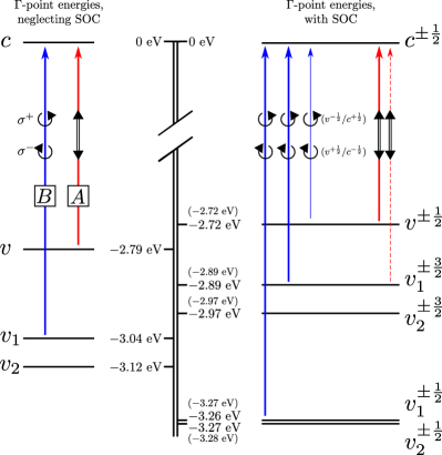
By diagonalizing in Eq. (1) and comparing the band energies with those found from DFT with SOC, Table 2, we find that eV and eV. The SOC-induced changes to the band energies at are illustrated in Fig. 1, showing good agreement between the DFT and bands. Note that inspection of the wavefunction decomposition of the conduction band edge with SOC shows a negligible () contribution from orbitals (which are present due to the hybridization of and ), so we neglect the effect of in our analysis, and use the conduction band edge as a reference energy, set at 0 eV. In contrast, hybridization is retained in the model as a significant effect. We find that perturbation theory overestimates the weight of band orbitals admixed into ,
| (2) |
as compared to found from numerical exact diagonalization of the Hamiltonian in Eq. (1).
(b) Band energies from a DFT calculation with SOC included, superscripts denote the components of total angular momentum () of the bands. (c) SOC constants for , Eq. (1), determined from fitting of -point bands from diagonalized Hamiltonian to DFT energies with and without SOC.
| (a) | |
|---|---|
| 0 eV | |
| 0.19 | |
| eV | |
| eVÅ2 | |
| eVÅ4 | |
| eV | |
| eV | |
| Å | |
| (b) | |
|---|---|
| 0 eV | |
| eV | |
| eV | |
| eV | |
| eV | |
| eV | |
| (c) | |
|---|---|
| 0.30 eV | |
| 0.30 eV | |
| 0.25 eV | |
In the absence of SOC, the coupling of the principal interband transition, , to in-plane polarized light is forbidden due to the opposite symmetry of and under , and also due to the lack of an orbital angular momentum difference between the bands. The coupling of to the lower branch of by SOC relaxes this selection rule, allowing coupling to in-plane polarized light. The transitions will be between total angular momentum states , coupling to -polarized photons. Since changes negligibly on application of SOC, we can consider the spin-projection to remain a good quantum number in the conduction band, and make the observation that -polarized light will excite electrons into spin up/down states in the conduction band, as sketched in the right hand side of Fig. 1.
For coupling of the principal interband transition to in-plane polarized light, we can estimate it as
| (3) |
where correspond to the vector potential of circularly polarized light, and is the weight of orbitals from admixed in the dominantly orbital based -band wavefunction. The oscillator strength of such transitions can be estimated as Å leading to the absorption coefficientMagorrian et al. (2016) for light incident perpendicular to the 2D crystal,
| (4) |
For comparison Magorrian et al. (2016), a photon incident at an angle to the surface and coupled to the the principal interband transition via the interband out-of-plane electric dipole moment, , is absorbed with , while for the B-line .
III Multilayers
Going on from the monolayerZhuang and Hennig (2013); Rybkovskiy et al. (2014); Magorrian et al. (2016); *tb_erratum; Zólyomi et al. (2014); Zhou et al. (2017); Debbichi et al. (2015); Jalilian and Safari (2017); Xiao et al. (2017); Demirci et al. (2017); Wickramaratne et al. (2015); Cai et al. (2017); Hung et al. (2017); Do et al. (2015); Li and Appelbaum (2015b); Nissimagoudar et al. (2017); Ayadi et al. (2017); Li et al. (2017) to -layer films, interlayer hopping between successive layers of InSe splits each band into subbands, as studied earlier using DFT and tight-binding calculationsMagorrian et al. (2016); Rybkovskiy et al. (2014); Mudd et al. (2016). At the -point, and split very weakly, whereas and , which are dominated by and orbitals on In and Se, exhibit a much stronger splitting. This moves the valence band edge (the top sub-band of ) further away from , reducing the effect of SOC on the band edge states. This weakening in the effect of SOC, anticipated from a perturbation theory analysis similar to Eq. (2), reduces the oscillator strengths of the spin-flip interband transitions. To describe quantitatively the spin-flip transitions in a multilayer film we employ a hopping model for few-layer InSe,
| (5) | ||||
Here, the operator annihilates (creates) an electron in band , spin state , in layer of the -layer crystal. The sum over runs twice over the bands included in the monolayer Hamiltonian in Eq. (1), and are the matrix elements of between band with spin projection and band with spin projection . The parameters eV, eV, and eV are interlayer hoppings, and eV and eV (which we neglect as it is much smaller than the interlayer hoppings) are onsite energy shifts due to interlayer potentials; all of these were determined from fitting of the -point energies obtained from Eq. (5) to the DFT sub-bands in 2-5 layer InSe Magorrian et al. (2016). Diagonalization of allows us to find the wavefunction and hence the -dependence of the absorption coefficient for in-plane polarized light for the optical transition across the principal band gap of -layer InSe;
| (6) |
where and are the -layer conduction-band effective mass and band gap, respectively, and is the total weight of all orbitals from sub-bands of admixed by SOC into the highest energy valence sub-band. Overall we find
| (7) |
see Table 3. This compares with an increase in from in the monolayer to for large , and with a roughly constant absorption for the B-line Magorrian et al. (2016).
| (eV) | (%) | (%) | (%) | |
|---|---|---|---|---|
| 2.72 | 1.5 | 3.7 | ||
| 2.00 | 6.4 | |||
| 1.67 | 8.2 | |||
| 1.50 | 9.6 | |||
| 1.40 | 10.7 |
IV Nuclear spin pumping
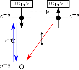
The excitation of electrons into states of the conduction band by -polarized light tuned to the energy of the principal interband transition allows for the optical pumping of In nuclear spins. This would occur through the mechanism sketched in Fig. 2. An electron excited by -polarized light into the conduction band state, leaving behind a hole in the valence band, , can transfer its spin to the nucleus via the hyperfine interaction, , where is the -component of the indium’s nuclear spin. After that, it can recombine without spin-flip with the photoexcited hole, with a similar cycle to be repeated following the absorption of the next -polarized photon.
A strong contribution of an indium orbital to the conduction band states presents the possibility of a strong coupling between the electronic spin and In nuclear spins. The most common isotope of indium, , has a nuclear spin , and an atomic hyperfine coupling constant Braun et al. (2006) (in comparison with Se, for which the only stable nucleus with non-zero spin, , , abundance 7%, has a much smaller coupling constant Zijlstra et al. (1972)). Using the orbital decomposition reported in Ref. Magorrian et al., 2016 we can estimate an effective hyperfine coupling constant for the conduction band, , where is the weight of In orbitals in the conduction band state near the -point. As a result, one can expect that monolayers and bilayers of InSe will offer a suitable material for achieving a high degree of optically induced nuclear spin polarization.
V Conclusions
In conclusion, we have used a model to show how spin-orbit coupling in mono- and few-layer InSe allows coupling between the principal interband transition and in-plane polarized light, accompanied by a spin-flip, with the coupling at its strongest in the monolayer, , saturating to for layers. We would expect a similar effect in the other III-VI semiconductors, such as GaSe, with the strength primarily determined by the SOC strength in the group VI atoms. Electrons, excited selectively into spin up/down states in the conduction band using -polarized light, can transfer their spin angular momentum to the In nuclei , allowing for optically induced nuclear spin polarization. The model presented here can be amended to include the effect on optical transitions in few-layer InSe of an applied displacement field in a dielectric environment, through changes to the onsite band energies and coupling to states in the dielectric environment, and this will be addressed in future work.
Acknowledgements.
The authors thank A. Patanè, A. V. Tyurnina, M. Potemski, Y. Ye, J. Lischner, and N. D. Drummond for discussions. This work made use of the facilities the CSF cluster of the University of Manchester. SJM acknowledges support from EPSRC CDT Graphene NOWNANO EP/L01548X. VF acknowledges support from ERC Synergy Grant Hetero2D, EPSRC EP/N010345, and Lloyd Register Foundation Nanotechnology grant. VZ and VF acknowledge support from the European Graphene Flagship Project, the N8 Polaris service, the use of the ARCHER national UK supercomputer (RAP Project e547), and the Tianhe-2 Supercomputer at NUDT. Research data is available from the authors on request.References
- Mak et al. (2010) K. F. Mak, C. Lee, J. Hone, J. Shan, and T. F. Heinz, Physical Review Letters 105, 136805 (2010).
- Splendiani et al. (2010) A. Splendiani, L. Sun, Y. Zhang, T. Li, J. Kim, C.-Y. Chim, G. Galli, and F. Wang, Nano Letters 10, 1271 (2010).
- Korn et al. (2011) T. Korn, S. Heydrich, M. Hirmer, J. Schmutzler, and C. Schüller, Applied Physics Letters 99, 102109 (2011).
- Wang et al. (2012) Q. H. Wang, K. Kalantar-Zadeh, A. Kis, J. N. Coleman, and M. S. Strano, Nature Nanotechnology 7, 699 (2012).
- Xu et al. (2014) X. Xu, W. Yao, D. Xiao, and T. F. Heinz, Nature Physics 10, 343 (2014).
- Jones et al. (2013) A. M. Jones, H. Yu, N. J. Ghimire, S. Wu, G. Aivazian, J. S. Ross, B. Zhao, J. Yan, D. G. Mandrus, D. Xiao, W. Yao, and X. Xu, Nature Nanotechnology 8, 634 (2013).
- Gan et al. (2013) X. Gan, Y. Gao, K. F. Mak, X. Yao, R.-J. Shiue, A. van der Zande, M. E. Trusheim, F. Hatami, T. F. Heinz, J. Hone, and D. Englund, Applied Physics Letters 103, 181119 (2013).
- Wu et al. (2014) S. Wu, S. Buckley, A. M. Jones, J. S. Ross, N. J. Ghimire, J. Yan, D. G. Mandrus, W. Yao, F. Hatami, J. Vučković, A. Majumdar, and X. Xu, 2D Materials 1, 011001 (2014).
- Sie et al. (2015) E. J. Sie, J. W. McIver, Y.-H. Lee, L. Fu, J. Kong, and N. Gedik, Nature Materials 14, 290 (2015).
- Wang et al. (2015) G. Wang, X. Marie, I. Gerber, T. Amand, D. Lagarde, L. Bouet, M. Vidal, A. Balocchi, and B. Urbaszek, Physical Review Letters 114, 097403 (2015).
- Liu et al. (2015) X. Liu, T. Galfsky, Z. Sun, F. Xia, E.-c. Lin, Y.-H. Lee, S. Kéna-Cohen, and V. M. Menon, Nature Photonics 9, 30 (2015).
- Zhou et al. (2015) X. Zhou, J. Cheng, Y. Zhou, T. Cao, H. Hong, Z. Liao, S. Wu, H. Peng, K. Liu, and D. Yu, Journal of the American Chemical Society 137, 7994 (2015).
- Jie et al. (2015) W. Jie, X. Chen, D. Li, L. Xie, Y. Y. Hui, S. P. Lau, X. Cui, and J. Hao, Angewandte Chemie International Edition 54, 1185 (2015).
- Hu et al. (2012) P. Hu, Z. Wen, L. Wang, P. Tan, and K. Xiao, ACS Nano 6, 5988 (2012).
- Late et al. (2012) D. J. Late, B. Liu, J. Luo, A. Yan, H. Matte, M. Grayson, C. Rao, and V. P. Dravid, Advanced Materials 24, 3549 (2012).
- Lei et al. (2013) S. Lei, L. Ge, Z. Liu, S. Najmaei, G. Shi, G. You, J. Lou, R. Vajtai, and P. M. Ajayan, Nano Letters 13, 2777 (2013).
- Aziza et al. (2017) Z. Ben Aziza, D. Pierucci, H. Henck, M. G. Silly, C. David, M. Yoon, F. Sirotti, K. Xiao, M. Eddrief, J.-C. Girard, and A. Ouerghi, Physical Review B 96, 035407 (2017).
- Jung et al. (2015) C. S. Jung, F. Shojaei, K. Park, J. Y. Oh, H. S. Im, D. M. Jang, J. Park, and H. S. Kang, ACS Nano 9, 9585 (2015).
- Pozo-Zamudio et al. (2015) O. D. Pozo-Zamudio, S. Schwarz, M. Sich, I. A. Akimov, M. Bayer, R. C. Schofield, E. A. Chekhovich, B. J. Robinson, N. D. Kay, O. V. Kolosov, A. I. Dmitriev, G. V. Lashkarev, D. N. Borisenko, N. N. Kolesnikov, and A. I. Tartakovskii, 2D Materials 2, 035010 (2015).
- Liu et al. (2014) F. Liu, H. Shimotani, H. Shang, T. Kanagasekaran, V. Zólyomi, N. D. Drummond, V. I. Fal’ko, and K. Tanigaki, ACS Nano 8, 752 (2014).
- Hu et al. (2014) P. Hu, J. Zhang, M. Yoon, X.-F. Qiao, X. Zhang, W. Feng, P. Tan, W. Zheng, J. Liu, X. Wang, J. C. Idrobo, D. B. Geohegan, and K. Xiao, Nano Research 7, 694 (2014).
- Huang et al. (2016) S. Huang, Y. Tatsumi, X. Ling, H. Guo, Z. Wang, G. Watson, A. A. Puretzky, D. B. Geohegan, J. Kong, J. Li, T. Yang, R. Saito, and M. S. Dresselhaus, ACS Nano 10, 8964 (2016).
- Lei et al. (2014) S. Lei, L. Ge, S. Najmaei, A. George, R. Kappera, J. Lou, M. Chhowalla, H. Yamaguchi, G. Gupta, R. Vajtai, A. D. Mohite, and P. M. Ajayan, ACS Nano 8, 1263 (2014).
- Mudd et al. (2013) G. W. Mudd, S. A. Svatek, T. Ren, A. Patanè, O. Makarovsky, L. Eaves, P. H. Beton, Z. D. Kovalyuk, G. V. Lashkarev, Z. R. Kudrynskyi, and A. I. Dmitriev, Advanced Materials 25, 5714 (2013).
- Mudd et al. (2014) G. W. Mudd, A. Patanè, Z. R. Kudrynskyi, M. W. Fay, O. Makarovsky, L. Eaves, Z. D. Kovalyuk, V. Zólyomi, and V. Fal’ko, Applied Physics Letters 105, 221909 (2014).
- Mudd et al. (2015) G. W. Mudd, S. A. Svatek, L. Hague, O. Makarovsky, Z. R. Kudrynskyi, C. J. Mellor, P. H. Beton, L. Eaves, K. S. Novoselov, Z. D. Kovalyuk, E. E. Vdovin, A. J. Marsden, N. R. Wilson, and A. Patanè, Advanced Materials 27, 3760 (2015).
- Tamalampudi et al. (2014) S. R. Tamalampudi, Y.-Y. Lu, R. Kumar U, R. Sankar, C.-D. Liao, K. Moorthy B, C.-H. Cheng, F. C. Chou, and Y.-T. Chen, Nano Letters 14, 2800 (2014).
- Balakrishnan et al. (2014) N. Balakrishnan, Z. R. Kudrynskyi, M. W. Fay, G. W. Mudd, S. A. Svatek, O. Makarovsky, Z. D. Kovalyuk, L. Eaves, P. H. Beton, and A. Patanè, Advanced Optical Materials 2, 1064 (2014).
- Yan et al. (2017) F. Yan, L. Zhao, A. Patanè, P. Hu, X. Wei, D. Zhang, Q. Lv, Q. Feng, C. Shen, K. Chang, L. Eaves, and K. Wang, Nanotechnology 28, 27LT01 (2017).
- Bandurin et al. (2017) D. A. Bandurin, A. V. Tyurnina, L. Y. Geliang, A. Mishchenko, V. Zólyomi, S. V. Morozov, R. K. Kumar, R. V. Gorbachev, Z. R. Kudrynskyi, S. Pezzini, Z. D. Kovalyuk, U. Zeilter, K. S. Novoselov, A. Patanè, L. Eaves, I. I. Grigorieva, V. I. Fal’ko, A. K. Geim, and Y. Cao, Nature Nanotechnology 12, 223 (2017).
- Mudd et al. (2016) G. W. Mudd, M. R. Molas, X. Chen, V. Zólyomi, K. Nogajewski, Z. R. Kudrynskyi, Z. D. Kovalyuk, G. Yusa, O. Makarovsky, L. Eaves, M. Potemski, V. I. Fal’ko, and A. Patanè, Scientific Reports 6, 39619 (2016).
- Zhuang and Hennig (2013) H. L. Zhuang and R. G. Hennig, Chemistry of Materials 25, 3232 (2013).
- Rybkovskiy et al. (2014) D. V. Rybkovskiy, A. V. Osadchy, and E. D. Obraztsova, Physical Review B 90, 235302 (2014).
- Zólyomi et al. (2014) V. Zólyomi, N. D. Drummond, and V. I. Fal’ko, Physical Review B 89, 205416 (2014).
- Debbichi et al. (2015) L. Debbichi, O. Eriksson, and S. Lebègue, The Journal of Physical Chemistry Letters 6, 3098 (2015).
- Wickramaratne et al. (2015) D. Wickramaratne, F. Zahid, and R. K. Lake, Journal of Applied Physics 118, 075101 (2015).
- Do et al. (2015) D. T. Do, S. D. Mahanti, and C. W. Lai, Scientific Reports 5 (2015).
- Li and Appelbaum (2015b) P. Li and I. Appelbaum, Physical Review B 92, 195129 (2015b).
- Magorrian et al. (2016) S. J. Magorrian, V. Zólyomi, and V. I. Fal’ko, Physical Review B 94, 245431 (2016).
- Magorrian et al. (2017) S. J. Magorrian, V. Zólyomi, and V. I. Fal’ko, Physical Review B 96, 079905(E) (2017).
- Zhou et al. (2017) M. Zhou, R. Zhang, J. Sun, W.-K. Lou, D. Zhang, W. Yang, and K. Chang, Physical Review B 96, 155430 (2017).
- Jalilian and Safari (2017) J. Jalilian and M. Safari, Physics Letters A 381, 1313 (2017).
- Xiao et al. (2017) K. J. Xiao, A. Carvalho, and A. H. Castro Neto, Physical Review B 96, 054112 (2017).
- Demirci et al. (2017) S. Demirci, N. Avazlı, E. Durgun, and S. Cahangirov, Physical Review B 95, 115409 (2017).
- Cai et al. (2017) Y. Cai, G. Zhang, and Y.-W. Zhang, The Journal of Physical Chemistry C 121, 10182 (2017).
- Hung et al. (2017) N. T. Hung, A. R. T. Nugraha, and R. Saito, Applied Physics Letters 111, 092107 (2017).
- Nissimagoudar et al. (2017) A. S. Nissimagoudar, J. Ma, Y. Chen, and W. Li, Journal of Physics: Condensed Matter 29, 335702 (2017).
- Ayadi et al. (2017) T. Ayadi, L. Debbichi, M. Said, and S. Lebègue, The Journal of Chemical Physics 147, 114701 (2017).
- Li et al. (2017) X. Li, J. Du, L. Wang, W. Xiong, T. Wang, and C. Xia, Physica E: Low-dimensional Systems and Nanostructures 94, 153 (2017).
- Note (1) Although in the absence of SOC this term is not relevant for the optical properties of InSe, it becomes important for the analysis of the effect of SOC on the principal interband transition.
- Zólyomi et al. (2013) V. Zólyomi, N. D. Drummond, and V. I. Fal’ko, Physical Review B 87, 195403 (2013).
- Cao et al. (2015b) T. Cao, Z. Li, and S. G. Louie, Physical Review Letters 114, 236602 (2015b).
- Chen et al. (2015) H. Chen, Y. Li, L. Huang, and J. Li, The Journal of Physical Chemistry C 119, 29148 (2015).
- Feng et al. (2016) W. Feng, G.-Y. Guo, and Y. Yao, 2D Materials 4, 015017 (2016).
- Si et al. (2016) C. Si, Z. Lin, J. Zhou, and Z. Sun, 2D Materials 4, 015027 (2016).
- Kresse and Furthmüller (1996) G. Kresse and J. Furthmüller, Physical Review B 54, 11169 (1996).
- Braun et al. (2006) P.-F. Braun, B. Urbaszek, T. Amand, X. Marie, O. Krebs, B. Eble, A. Lemaitre, and P. Voisin, Physical Review B 74, 245306 (2006).
- Zijlstra et al. (1972) W. Zijlstra, J. Henrichs, and J. V. Voorst, Chemical Physics Letters 13, 325 (1972).