Band structure and giant Stark effect in two-dimensional transition-metal dichalcogenides
Abstract
We present a comprehensive study of the electronic structures of 192 configurations of 39 stable, layered, transition-metal dichalcogenides using density-functional theory. We show detailed investigations of their monolayer, bilayer, and trilayer structures’ valence-band maxima, conduction-band minima, and band gap responses to transverse electric fields. We also report the critical fields where semiconductor-to-metal phase transitions occur. Our results show that band gap engineering by applying electric fields can be an effective strategy to modulate the electronic properties of transition-metal dichalcogenides for next-generation device applications.
I Introduction
Recent advances in the development of atomically-thin materials have opened up new possibilities to explore a two-dimensional (2D) semiconducting era Novoselov et al. (2005); Splendiani et al. (2010); Geim and Novoselov (2007); Qian et al. (2015); Golberg et al. (2010); Osada and Sasaki (2009); Wang et al. (2012a); Akinwande et al. (2014). Among 2D materials, transition-metal dichalcogenides (TMDCs) are an interesting family with a diverse range of material properties varying from metals to insulators Mak and Shan (2016). TMDCs have general formula MX2, where M is a transition metal and X is a chalcogen. (In this article, we include oxygen in the chalcogens for brevity of expression.) In MX2, there is a layer of metal atoms sandwiched between two layers of chalcogen atoms in a X–M–X pattern Wang et al. (2012b); Xiao et al. (2012).
Many of the semiconducting, layered TMDCs have similar general features. Their band gaps widen with decreasing number of layers. For example, by reducing the number of layers from bulk down to a single layer, the band gap of MoS2 switches from an indirect band gap of 1.28 eV to a direct band gap of 1.80 eV Mak et al. (2010); Splendiani et al. (2010) due to the stronger quantum confinement in the vertical direction. This band gap tunability via the layer thickness provides further avenues for novel nanoelectronics and nanophotonics applications Mak et al. (2010); Splendiani et al. (2010).
A tunable band gap is highly desirable to allow design flexibility and to control the properties of electronic devices, e.g., single-electron transistors Angus et al. (2007); Javaid et al. (2017); Sun et al. (2009), to achieve tunable fluorescence, display technology, and in changing electrical conductivity applications etc. Simon M. Sze (2006). However, after fabrication the layer thickness cannot be varied to further tune the band gap. One possible way to control the device properties after the fabrication process is to tune the band structure using external transverse electric fields Lu et al. (2014); Xu et al. (2013); Balu et al. (2012).
Two-dimensional semiconductors are also good candidates for photocatalytic water applications due to their large specific surface area, excellent light absorption, and tunable electronic properties Yeh et al. (2014); Singh et al. (2015). It has been reported in Rasmussen and Thygesen (2015) that many of the TMDCs qualify for water-splitting applications.
In the present work, our goal is to explore the band structure modification via electric field of as many stable, layered, predominately semiconducting TMDCs as possible. Around 40 of the layered TMDCs were reported by Wilson et al. in the 1960s Wilson and Yoffe (1969) and reviewed recently by Kuc et al. Kuc et al. (2015). They reported the bulk structures and electrical characteristics of the H and/or T phases of ScS2, ScSe2, ScTe2, TiS2, TiSe2, TiTe2, ZrS2, HfS2, HfSe2, VS2, VSe2, VTe2, NbS2, NbSe2, NbTe2, TaS2, TaSe2, TaTe2, CrS2, CrSe2, CrTe2, MoS2, MoSe2, MoTe2, WS2, WSe2, WTe2, MnS2, MnSe2, MnTe2, ReS2, ReSe2, ReTe2, FeS2, FeSe2, FeTe2, NiS2, NiSe2, NiTe2, and PdS2. There have been significant efforts to synthesize single and multilayer nanosheets from bulk structures, e.g., TiS2, ZrS2, NbSe2, TaS2, TaSe2, MoS2, MoSe2, MoTe2, WS2, WSe2, WTe2, ReS2, ReSe2, and NiTe2 have been grown by various methods Ugeda et al. (2016, 2014); Barja et al. (2016); Dumcenco et al. (2015a); Wang et al. (2014); Chang et al. (2014); Chen et al. (2015); Yoshida et al. (2016); Chung et al. (1998); Keyshar et al. (2015); Hafeez et al. (2016); Naylor et al. (2016); Zhou et al. (2017); Dumcenco et al. (2015b); Eichfeld et al. (2015); Gao et al. (2015); Coleman et al. (2011); Zeng et al. ; Zhan et al. ; Lin et al. (2012); Ennaoui et al. (1995); Kang et al. (2015); Zhang et al. (2013); Shaw et al. (2014); Lee et al. (2012) and discussed in recent reviews of TMDCs Chhowalla et al. (2013); Manzeli et al. (2017); Duan et al. (2015). Our current work also explores those TMDC monolayers and multilayers which have not yet been synthesized but have been predicted to be stable, layered, and semiconducting.
Molybdenum- and tungsten-based dichalcogenides have been intensively investigated. The band gap variation of a few layers of these materials under electric field have been widely studied Ramasubramaniam et al. (2011); Liu et al. (2012); Nguyen et al. (2016); Kuc et al. (2015); Lanzillo et al. (2016); Li et al. (2016); Yuan et al. (2013); Dai et al. (2015). Lebègue et al. Lebègue et al. (2013) have reported 2D materials by data filtering from their known bulk structures. The band gaps of monolayers of the stable, layered TMDCs have been reported by Ataca et al. in Ataca et al. (2012) and later by Rasmussen et al. in Rasmussen and Thygesen (2015). However, to date there has been no comprehensive study of the band structure responses of the stable, semiconducting, few-layer TMDCs to electric fields.
In this article, we study the role of transverse electric field in engineering band gaps in the known, stable, predominately semiconducting, few-layer TMDCs. We also study responses of their valence-band maxima (VBM) and the conduction-band minima (CBM) with electric field. This is of especial significance for device design and the optimization of atomically thin optoelectronic systems Simon M. Sze (2006); Linke et al. (2000); Angus et al. (2007).
This paper is organized as follows: In Section II, we describe the computational details. Then we discuss the electronic structures in Sec. III, followed by the lattice parameters and the band gap analysis at zero field in Sec. III A. Then we discuss the variations of the band gaps under field for monolayer, bilayer, and trilayer TMDCs in Sec. III B followed by the discussion of the responses of the VBM and CBM to the electric field in Sec. III C.
II Computational details
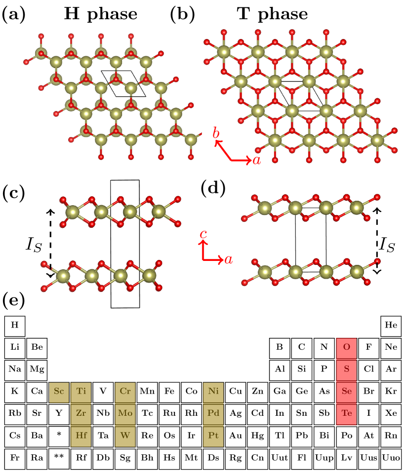
We studied TMDCs constructed by combining transition metals (brown-highlighted) and chalcogens (red-highlighted) in the periodic table as shown in Fig. 1(e). We studied two different structures: honeycomb (H) crystal structures with hexagonal space group P63/mmc and centred honeycomb (T) crystal structures with trigonal space group Pm1. Both of these structures and their unit cells are shown in Fig. 1.
All the calculations were performed using zero-Kelvin, density-functional theory (DFT) in the crystal09 code Dovesi et al. (2005, 2013). The lattice constants of the bulk structures were determined by structure relaxation using the PBEsol functional Perdew et al. (2008) for both exchange and correlation terms. The PBEsol functional generally predicts lattice constants more accurately than PBE and LSDA (thus better approximating the equilibrium properties of solids), and also handles the electronic response to potentials better than most GGA functionals Perdew et al. (2008). We compared our computed lattice parameter with the experimental values where available. We did not find a difference larger than 5% between the experimental and our computed values, indicating that the PBEsol functional is reasonably calculating this parameter. As there are no published van der Waals correction factors for third-row transition metals Grimme (2006), we ignored these corrections to keep our calculations consistent for all studied materials.
The geometries were optimized to the default crystal09 convergence criteria of less than 4.5 Hartree/Bohr maximum force, 3 Hartree/Bohr RMS force, 1.8 Hartree maximum displacement, and 1.2 Hartree RMS displacement.
We used Gaussian basis sets; triple-zeta for valence electrons plus a polarization function (TZVP) for the lighter elements (third-period metals and all chalcogens but Te) and pseudopotential basis sets for the heavy elements as follows: Sc_pob_TZVP_2012 Peintinger et al. (2013) for Sc, Ti_pob_TZVP_2012 for Ti Peintinger et al. (2013), Zr_ECP_HAYWSC_311d31G_dovesi_1998 Bredow and Lerch (2004) for Zr, Hf_ECP_Stevens_411d31G_munoz_2007 Muñoz Ramo et al. (2007) for Hf, Cr_pob_TZVP_2012 Peintinger et al. (2013) for Cr, Mo_SC_HAYWSC-311(d31)G_cora_1997 Corà et al. (1997) for Mo, W_cora_1996 Corà et al. (1996) for W, Ni_pob_TZVP_2012 Peintinger et al. (2013) for Ni, Pd_HAYWSC-2111d31_kokalj_1998_unpub Kokalj et al. (2002) for Pd, Pt_doll_2004 Doll (2004) for Pt, O_pob_TZVP_2012 Peintinger et al. (2013) for O, S_pob_TZVP_2012 Peintinger et al. (2013) for S, Se_pob_TZVP_2012 Peintinger et al. (2013) for Se, and Te_m-pVDZ-PP_Heyd_2005 Heyd et al. (2005) for Te.
We created the monolayer, bilayer, and trilayer TMDC unit slabs by defining (001) planes from bulk models, and including vacuum to a total cell height of Å. We set an 8161 Monkhorst-Pack Monkhorst and Pack (1976) -point mesh. We optimized the geometries of monolayer, bilayer, and trilayer TMDC unit slabs under zero electric field. We used these zero-field-optimized geometries to study the effects of transverse electric fields on their band structures as the influence of field-based geometric disturbances on the band structures is negligible Liu et al. (2012). We also checked the effects of electric field on the interlayer separation in H-TiO2 and H-MoS2 bilayer structures and found that the electric fields used do not modify the optimal interlayer separations of these structures.
The applied field strength was consistently varied from 0 to 0.2 V/Å as discussed later in the relevant sections. To compute the critical field (where the semiconductor-to-metal phase transition occurs), we further increased the field strength above 0.2 V/Å until we reached the field value where the band gap closed, except for those materials that have critical fields smaller than 0.2 V/Å.
We calculated the band structures along the high-symmetry path -M-K-. Band structures were calculated for uniformly varying electric fields applied perpendicular to the TMDC slabs.
III Results and discussion
In this section, we present our electronic structure calculations. For all the TMDC materials under investigation, we computed the relaxed bulk (three-dimensional) structure parameters (the in-plane lattice parameters or unit-cell lengths () and the unit-cell lengths () perpendicular to the plane), the interlayer separations , and band gaps of the bulk structures without electric field. We then computed the band gaps of the relaxed monolayer, bilayer, and trilayer structures with and without electric field along the directions. We discuss the band gaps’ modulation, the critical fields where the semiconductor-to-metal phase transition occurs and the responses of the VBMs and CBMs under electric field. We report our computed parameters in Table 3 (which is at the end of the document due to its considerable length). We also report the published values of the monolayer, bilayer, and trilayer structures’ band gaps at zero field, band gap variations under field, and the critical field where available. Throughout the discussion, we focus more on the trends observed across the TMDC family, in various ways, instead of the in-depth analysis of individual materials.
III.1 Properties under zero field
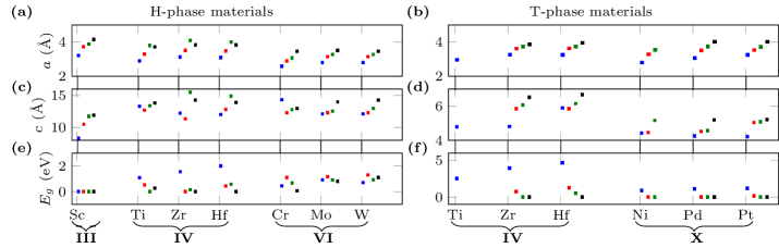
For several of the materials (H-ScX2, T-ZrX2, T-NiX2, T-PdX2, and T-PtX2), we observe increasing bulk structure lattice parameters and as we move down the chalcogen group from oxides to tellurides, accompanied by decreasing band gaps (Fig. 2), as reported in Table 3. The other materials depart from this trend in various ways, to various extents. For example, H-MoX2 and H-WX2 follow this trend for both their lattice parameters but their bulk band gaps from oxides to tellurides do not. H-CrX2 follow an increasing trend in the lattice parameter but not in . Also their bulk band gaps appear non-linear with respect to chalcogen element. T-HfX2 follow the trend in and the bulk band gaps but T-HfS2 deviates for . H-ZrX2, H-HfX2 and H-TiX2 show deviation from this general trend across all of the parameters, i.e., , , and the bulk band gaps. A similar oxide to telluride trend in TMDC monolayer band gaps has been reported by Rasmussen et al. Rasmussen and Thygesen (2015). No major trends in the lattice parameters or bulk band gaps are observed either across the periods or down the groups in the transition metals (Fig. 2).
Companion analyses have been carried out by instead changing the transition metal period (3, 4, and 5), transition metal group (III, IV, VI, and X), the material phase (H and T), or the number of layers in the model (1, 2, or 3), while holding all other dimensions constant. The number of non-singleton, non-zero-valued, subset classes for each dimension are: varying chalcogen, varying transition-metal period, varying transition-metal group, varying material phase, and varying the number of layers. Note: the numbers in parentheses indicate the number of members of each class.
The results are summarised in Table 1, which shows the dominant behavior (or the two, most-prevalent, non-dominant behaviors) across all subset classes with more than one element. The behaviors considered are: flat (F), monotonically increasing (), monotonically decreasing (), or other non-monotonic behavior (X) for classes with more than two members.
| Variable | Parameter | |||
|---|---|---|---|---|
| Bulk | ||||
| Chalcogen | /Xa | X/ | ||
| TM period | /Xc | X/ | ||
| TM group | / | |||
| Phase | ||||
| Layers | F | F | F | |
-
•
a 50/50%; b 50/42%; c 50/38%; d 44/38%; e 43/38%; f 47/42%
Examining combinations of the trends (multi-parameter patterns), we found that with a change of phase (from H to T) 5 of 9 subsets showed a combined increase to , decrease to , and increasing band gap. With increasing transition-metal group, 10 of 21 subsets showed decreases to both and (but a 4/6 split between increasing and decreasing band gap). All other combinations accounted for smaller proportions of the subset classes and are therefore regarded as insignificant.
For most of the materials we find an increase in the band gap with the decreasing number of layers from bulk to monolayer which is consistent with the properties of the Mo- and W-based dichalcogenides Kuc et al. (2011). (Note there are too many values to show clearly in a figure, but their values are available in Table 3.) We observe minor deviations from this trend by H-ZrO2, H-ZrSe2, H-HfO2, T-HfO2, H-HfSe2, H-CrS2, H-CrSe2, H-CrTe2, H-MoO2, H-MoSe2, H-MoTe2, H-WO2, H-WTe2, T-NiO2, T-PdO2, and T-PtO2. For example, the band gap of H-ZrO2 increases from 1.54 eV to 2.08 eV from bulk to its bilayer structure but the monolayer has a smaller gap of 1.62 eV.
III.2 Band gap variations under electric field
An electric field can potentially be used to tailor the band gaps of layered materials. The band structure variations with electric field arise due to the well-known Stark effect. The Stark effect induces a potential difference between the layers which causes splitting of energy bands belonging to different layers as well as shifting of the VBM and CBM Liu et al. (2012). This splitting and shifting of the energy bands can increase Mak et al. (2009); Zhang et al. (2009); Ni et al. (2012) or reduce Chen et al. (2004); Ramasubramaniam et al. (2011) the band gaps. In the case of multilayered TMDCs, this splitting and shifting pushes both the CBM and VBM towards the Fermi level. This results in the reduction of the band gap with applied electric field in multilayered TMDCs.
For each material under investigation, we computed band gaps of its monolayer, bilayer, and trilayer structures with an external electric field applied perpendicular to the layers along the directions. We consistently varied the field strength from 0 to 0.2 V/Å, in steps no larger than 0.02 V/Å, except for materials (H-TiO2 trilayer, H-ZrSe2 bilayer, T-ZrSe2 trilayer, H-CrO2 bilayer and trilayer, H-CrTe2 bilayer, and H-WO2 trilayer) whose band gaps close before 0.2 V/Å. This maximum field strength is stronger than usual device fields and is shown to more clearly illustrate the band structure variations under electric field.
For all structures, we find that monolayer TMDCs do not respond to electric field up to a field strength of 0.2 V/Å. However the band structures of most of the bilayer and trilayer TMDCs do vary with electric field offering applications in band engineering. Such results are consistent with previously reported studies of Mo- and W-based dichalcongenides.
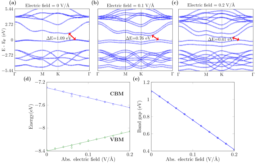
Figure 3 shows sample band structures of H-phase TiO2 bilayers at zero field and for two different finite values of the electric field. Increasing the electric field causes splittings of the energy bands resulting in a reduction of the band gap from 1.09 eV (at zero field) to 0.41 eV (at 0.2 V/Å). The responses of the VBM and CBM are shown in Fig. 3(d) for electric fields varying from 0 V/Å to 0.2 V/Å. There is significant variation of both the VBM and the CBM with the electric field pushing them towards the Fermi level, EF for the H-TiO2 bilayer resulting in the reduction of the band gap under field. The band gap as a function of the absolute electric field is shown in Fig. 3(e) where the solid line is a linear fit to the data. For an electric field of 0.2 V/Å, the band gap is reduced by 686 meV. Thus band gap variation in H-TiO2 bilayers is achievable via electric field at a rate of -3.43 eV/(V/Å) while the corresponding VBM and CBM bendings are 1.69 and -1.73 eV/(V/Å) respectively.
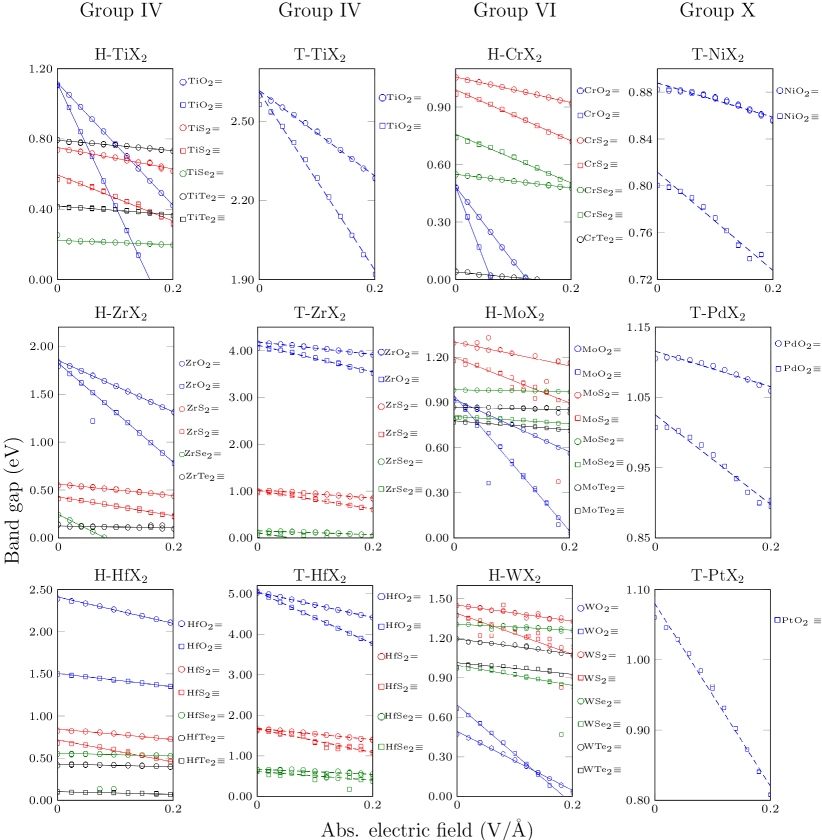
We obtain qualitatively similar band structure responses to electric field for most of the studied materials. The band gaps as functions of electric field are shown in Fig. 4 for all materials. Most band gaps decrease monotonically with electric field strength. The Ni, Pd, and Pt oxides seem to exhibit slightly quadratic behavior at low field which is similar to the band structure modulation via electric field reported for few layer black phosphorus Liu et al. (2017). The linear fits applied across all band gap data as functions of electric field (Fig. 4) are shown by solid lines for all H-phase materials and by dashed lines for all T-phase materials. Circular and square markers represent the bilayer and trilayer data in all the sub-figures while the blue, red, green, and black colors represent the oxides, sulphides, selenides, and tellurides respectively. All the materials show symmetric response to fields oriented in the directions which is due to the symmetry of the chalcogen layers around the metal layer, except a few odd data points (Fig. 4). We have excluded these odd data points from the linear fits as we believe that they do not represent the underlying physics.
The change in the band gap with the electric field, , is given by Ramasubramaniam et al. (2011)
| (1) |
Here is the band gap in eV, is the electric field strength in V/Å, is the fundamental charge, and is the GSE coefficient, calculated from the slope of the linear fits to our data shown in Fig. 4. We report this GSE coefficient () in Table 3 along with 95% confidence intervals. We compare our computed GSE coefficient with the literature where available in Table 3.
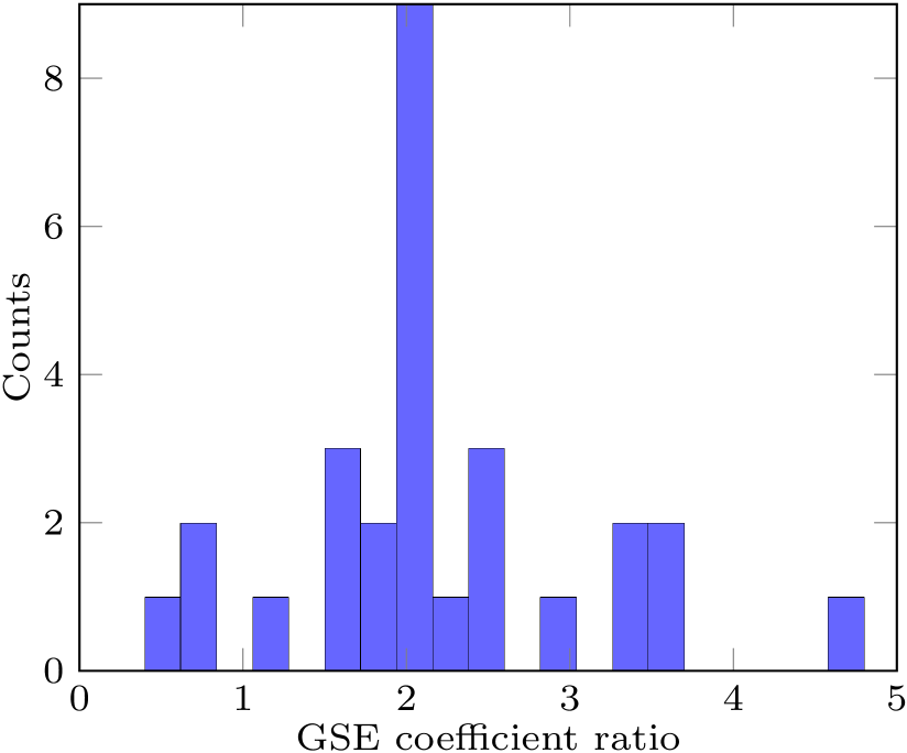
We observe an interesting trend in for the bilayer and trilayer structures of several materials. We find that the values for trilayer structures are approximately twice those for bilayer structures, with a few anomalies. For example, H-TiO2 trilayers has = 6.87 Å which is twice that of 3.43 Å for H-TiO2 bilayers. Similarly, H-CrO2 and H-CrS2 show a factor of two in between their trilayer and bilayer structures. We report this trilayer-bilayer ratio () in Table 3 and display it in histogram form in Fig. 5. The symbols and represent trilayer and bilayer structures respectively. A group of the materials cluster around a ratio of two with a few outliers. T-ZrSe2, H-HfO2, H-CrSe2, H-MoO2, H-MoSe2, H-WSe2, and T-NiO2 are outliers. The tellurides show anomalous behavior where they have non-zero band gaps in both bilayer and trilayer structures. Their ratios are smaller than the other dichalcogenides suggesting that telluride trilayers are less sensitive to field.
The near-double modulation of trilayer TMDCs compared to their associated bilayers might be explained by the number of interlayer separations () they have. Bilayers have one , while trilayers have two. Monolayers have none, and it is well established that they do not exhibit band gap variation (and therefore their ).
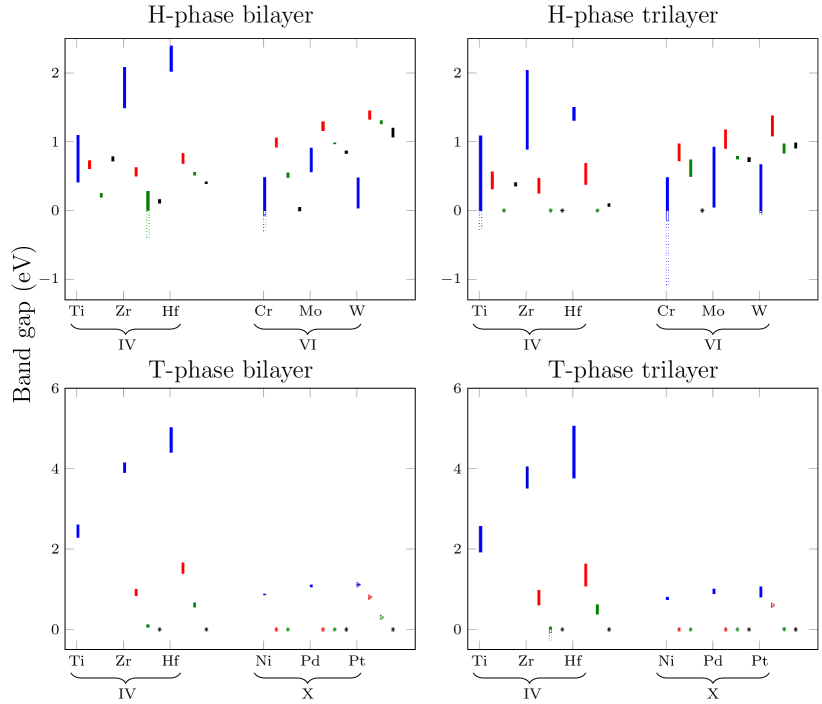
All studied materials’ band gap variations with field are shown in Fig. 6. The length of each bar shows the change in the band gap under field. The top of each rectangular bar shows the material’s band gap at zero field and the bottom of each rectangular bar shows the band gap at the maximum field of 0.2 V/Å or less for materials whose band gaps close before 0.2 V/Å. Blue, red, green, and black colors represent the oxides, sulphides, selenides, and tellurides. Rectangular bars crossing the zero-band-gap line indicate materials where the CBM switches below VBM at maximum field.
Table 2 details a multidimensional trend analysis for (and several other properties which are discussed below), similar to those for bulk properties presented in Table 1. The numbers of subset classes change due to the separation of materials by number of layers and subsequent exclusion of monolayer data or others whose are uniformly zero, along with any completely metallic or semi-metallic classes. For (and , , and , discussed below), there are subset classes varying chalcogen, classes varying transition-metal period, varying transition-metal group, varying phase, and varying layer number.
| Variable | Parameter | |||||||
|---|---|---|---|---|---|---|---|---|
| Chalcogen | X | X | X | X | X | /Xa | ||
| TM period | X | /Xb | /Xc | X/ | X | |||
| TM group | / | |||||||
| Phase | ||||||||
| Layers | ||||||||
-
•
a 48/48%; b 48/39%; c 44/34%; d 41/38%; e 47/37%.
We notice an overall decrease in band gap variation under field, , down the chalcogen group from the oxides to tellurides with a few anomalies. This trend is also illustrated in Fig. 6 where we can see a decrease in the bar lengths from oxides (blue) to tellurides (black) for most of the transition metals, which again suggest that tellurides are less sensitive to electric fields than other dichalcogenides.
behaves non-monotonically with transition-metal period, but decreases with transition-metal group. The group X TMDCs exhibit the least band gap variation under field when compared as a whole to other groups. For example, the PtO2 bilayer, the PtS2 and the PtSe2 bilayer and trilayer do not respond to the field within the range of 0.2 V/Å as compared to the Hf- and W-based dichalcogenides (Table 3).
The GSE coefficients increase from the H- to T-phase materials as shown in Fig. 6 for those materials which are stable in both H and T phases. This is mainly due to the distinct intralayer stacking of the two phases leading to a difference in the interplanar X–X dispersion interactions Kumar et al. (2015). Thus selection of the material phase is another potential pre-fabrication lever for controlling band gaps and their variations under field.
We further reveal the critical fields (), where closures of band gaps occur and the bilayer or trilayer TMDCs undergo semiconductor-to-metal phase transitions. To achieve this, we increased the field strengths beyond 0.2 V/Å for those materials whose band gaps had not yet closed. We report these computed critical fields in Table 3, and summarise their trends in Table 2.
The critical field strengths vary non-monotonically down the chalcogen group from oxides to tellurides. Similarly, no dominant trends in the critical field strengths are predicted across the transition metal periods or down the transition metal groups for the same phase, chalcogen, and number of layers. However, does increase from H- to T-phase materials, and and is generally lower for trilayer materials than the related bilayer ones.
The converse dependencies of and on transition-metal group or layer number are understandable; since corresponds to the slope of the band gap with field, it stands to reason that more responsive materials (trilayers) should become metallic or semi-metallic at lower fields (), particularly once account is taken of any discrepancy in their zero-field band gaps. However, the behavior with phase is aligned, with both parameters increasing. Comparison with Table 1 shows that this is explained by an evident accompanying increase in the zero-field band gaps with phase.
Our general findings are that: trilayer band gaps respond more to field than bilayer gaps; T-phase materials respond more than H-phase ones; band gap modulations decrease from oxides to tellurides; and the response to the electric field decreases from left to right across the transition metals when compared within the same period and for the same chalcogens. These findings reveal the whole range of TMDC band gap responses under field. They enable one to select the appropriate material(s) to engineer devices in according to one’s application’s requirements.
III.3 Valence and conduction band absolute positions and variations under field
For many applications, the energies of the valence and conduction bands with respect to the vacuum level are important. For example, in the construction of 2D heterostructure materials, knowledge of absolute VBM and CBM energies is required to predict behavior. For device design, such as a single-electron transistor Angus et al. (2007); Javaid et al. (2017), where we require control over its transport properties, study of the VBMs’ and CBMs’ responses to electric fields is essential.
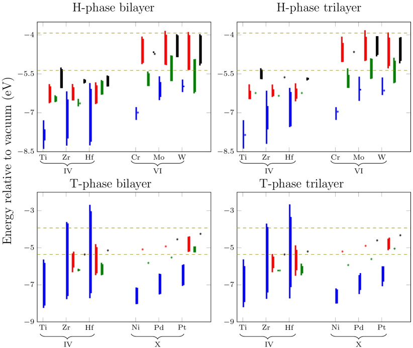
In Fig. 7, we show the computed energies of all studied TMDCs VBMs, and CBMs with respect to the vacuum – at zero field (left rectangular bar) and for the maximum field of 0.2 V/Å or less for those materials whose band gaps close before 0.2 V/Å (right rectangular bar). The lengths of the rectangular bars show the band gaps. The blue, red, green, and black colors show oxides, sulphides, selenides, and tellurides respectively.
We also summarise any trends in Table 2. Here, for the absolute energies, we have subset classes when varying chalcogen, varying transition-metal period, varying transition-metal group, varying phase, and varying layer number. The rates of change of the VBM and CBM have the same numbers and types of subset classes as and , described in Sec. III.2.
The absolute VBM and CBM energies behave non-monotonically as the chalcogen period increases. However, they largely increase with transition-metal period and group, and with changing from H to T phase. Whilst the zero-field extrema energies increase with the number of layers, the maximum-field extrema energies both decrease with layer number, consistent with the increased also exhibited by trilayer materials.
When changing transition metal period, 11 of 32 subset classes show an overall increases in all four reported VBM and CBM energies (Fig. 7 top panels). This behavior is particularly prominent in the oxides. 28 of 42 subset classes show the same behaviour when transition-metal group is changed (i.e., comparing same-colored bars between left and right groups in subfigures of Fig. 7). However, while increasing the number of layers 16 of 44 subset classes show increases to the zero-field extrema with decreases to the high-field extrema.
For almost all of these materials, we find significant bending in the CBM under field (as reported in Table 3 and shown in Fig. 7) except for a few materials, e.g., WSe2 bilayers and PdO2 trilayers show anomalous behavior; their CBMs increase with the field. The VBMs for all the materials show increasing energy shifts under electric field except TiTe2 bilayers, H-HfTe2 bilayers, CrTe2 bilayers, and MoS2 bilayers, which show a negative bending in their VBMs (Table 3).
Looking broadly across all parameters reported in Table 2, we identify the following large-scale compound behaviours: when varying transition-metal group, 10 of 42 subset classes show consistent behavior across all eight parameters – increases to all absolute energies plus combined with decreases to the other three parameters; when increasing the number of layers, 19 of 44 subsets show increasing and with decreasing and , 15 of 44 show increased and VBM energies (both fields) with decreased , and 23 of 44 show decreased with increased VBM energies (both fields). Other compound behaviours are only exhibited by small fractions of the subset classes.
It has been reported in Rasmussen and Thygesen (2015) that materials with CBMs above the standard hydrogen electrode (SHE), i.e. -4.03 eV relative to vacuum at pH 7, can be used at the cathode of photocatalytic water splitting devices to evolve hydrogen. Similarly materials with VBMs below the oxygen evolution potential (1.23 eV below the SHE) can be used as photoanodes in water splitting devices. It has been suggested that the CBM/VBM should lie a few tenths of an electron volt above/below the redox potentials Trasatti (1986) to account for the intrinsic energy barriers of the water splitting reactions Nørskov et al. (2004); Butler and Ginley (1978). Any material with a CBM a few tenths of an electron volt above -4.03 eV or VBM a few tenths of an electron volt below -5.26 eV is desirable for water splitting applications.
In Fig. 7, the CBMs of Mo- and W-based, bilayer and trilayer sulphides lie 0.1 eV above -4.03 eV at zero and low fields. For example, MoS2 bilayers have a useful CBM for water splitting applications in electric fields ranging from 0 to 0.14 V/Å. Similarly, MoS2 trilayers, WS2 bilayers, and WS2 trilayers are useful for this application in fields ranging from 0 to 0.04, 0.1, and 0.04 V/Å, respectively. The T-phase, Zr and Hf, bilayer and trilayer oxides have CBMs well above the SHE potential for both zero and maximum field and could be useful for water splitting applications under any field strength from 0 to 0.2 V/Å.
Most of the materials have their VBM below the oxygen redox potential except for the bilayers and trilayers of CrS2, CrTe2, MoS2, MoTe2, WS2, WTe2, PtS2, and PtSe2, and the zero band gap materials (Fig. 7). The TMDCs therefore appear to be a highly useful class of materials for water splitting.
IV Conclusions
We have presented a comprehensive density-functional theory study of the electronic structures of 192 configurations of 39 stable, two-dimensional, transition-metal dichalcogenides. Our calculations show the band gaps of few-layer TMDCs along with variation of the band structures by electric fields. The data has been analysed across five dimensions: chalcogen period, transition-metal period, transition-metal group, phase, and number of layers.
Band gaps generally decrease down the chalcogen group from oxides to tellurides, increase across the transition metals from left to right, are larger for T-phase materials than corresponding H-phase ones, and decrease with more layers. The responses to the electric field decrease down the chalcogens and across transition metals in the same period, are larger for T-phase materials than H-phase ones, and increase with increasing number of layers. We generally found that the CBMs decrease with higher fields while the VBMs increase, narrowing the band gap from both sides. We also have suggested materials which could be useful for water splitting applications under zero and low fields.
By presenting the field-modulated behavior of monolayer, bilayer, and trilayer structures of 39 different materials, this work supports the advance of 2D materials from fundamental research to real applications. In particular, it will aid band-gap and opto-electronic engineers to select the optimal TMDC for their device requirements.
Acknowledgements
The authors acknowledge financial support from the Australian Research Council (Project Nos. DP130104381, CE140100003, FT160100357, LE160100051, and CE170100026). This work was supported by computational resources provided by the Australian Government through the National Computational Infrastructure (NCI) under the National Computational Merit Allocation Scheme.
References
- Novoselov et al. (2005) K. S. Novoselov, A. K. Geim, S. V. Morozov, D. Jiang, M. I. Katsnelson, I. V. Grigorieva, S. V. Dubonos, and A. A. Firsov, Nature 438, 197 (2005).
- Splendiani et al. (2010) A. Splendiani, L. Sun, Y. Zhang, T. Li, J. Kim, C.-Y. Chim, G. Galli, and F. Wang, Nano Lett. 10, 1271 (2010).
- Geim and Novoselov (2007) A. K. Geim and K. S. Novoselov, Nat. Mater. 6, 183 (2007).
- Qian et al. (2015) X. Qian, Y. Wang, W. Li, J. Lu, and J. Li, 2D Mater. 2, 032003 (2015).
- Golberg et al. (2010) D. Golberg, Y. Bando, Y. Huang, T. Terao, M. Mitome, C. Tang, and C. Zhi, ACS Nano 4, 2979 (2010).
- Osada and Sasaki (2009) M. Osada and T. Sasaki, J. Mater. Chem. 19, 2503 (2009).
- Wang et al. (2012a) H. Wang, L. Yu, Y.-H. Lee, Y. Shi, A. Hsu, M. L. Chin, L.-J. Li, M. Dubey, J. Kong, and T. Palacios, Nano Lett. 12, 4674 (2012a).
- Akinwande et al. (2014) D. Akinwande, N. Petrone, and J. Hone, Nat. Commun. 5, 5678 (2014).
- Mak and Shan (2016) K. F. Mak and J. Shan, Nat. Photon 10, 216 (2016).
- Wang et al. (2012b) Q. H. Wang, K. Kalantar-Zadeh, A. Kis, J. N. Coleman, and M. S. Strano, Nat. Nanotechnol. 7, 699 (2012b).
- Xiao et al. (2012) D. Xiao, G.-B. Liu, W. Feng, X. Xu, and W. Yao, Phys. Rev. Lett. 108, 196802 (2012).
- Mak et al. (2010) K. F. Mak, C. Lee, J. Hone, J. Shan, and T. F. Heinz, Phys. Rev. Lett. 105, 136805 (2010).
- Angus et al. (2007) S. J. Angus, A. J. Ferguson, A. S. Dzurak, and R. G. Clark, Nano Lett. 7, 2051 (2007).
- Javaid et al. (2017) M. Javaid, D. W. Drumm, S. P. Russo, and A. D. Greentree, Nanotechnology 28, 125203 (2017).
- Sun et al. (2009) J. Sun, M. Larsson, I. Maximov, H. Hardtdegen, and H. Q. Xu, Appl. Phys. Lett. 94, 042114 (2009).
- Simon M. Sze (2006) K. K. N. Simon M. Sze, Physics of Semiconductor Devices, Edition 3 (John Wiley & Sons, 2006).
- Lu et al. (2014) N. Lu, H. Guo, L. Li, J. Dai, L. Wang, W.-N. Mei, X. Wu, and X. C. Zeng, Nanoscale 6, 2879 (2014).
- Xu et al. (2013) D. Xu, H. He, R. Pandey, and S. P. Karna, J. Phys.: Condens. Matter 25, 345302 (2013).
- Balu et al. (2012) R. Balu, X. Zhong, R. Pandey, and S. P. Karna, Appl. Phys. Lett. 100, 052104 (2012).
- Yeh et al. (2014) T.-F. Yeh, C.-Y. Teng, S.-J. Chen, and H. Teng, Adv. Mater. 26, 3297 (2014).
- Singh et al. (2015) A. K. Singh, K. Mathew, H. L. Zhuang, and R. G. Hennig, J. Phys. Chem. Lett. 6, 1087 (2015).
- Rasmussen and Thygesen (2015) F. A. Rasmussen and K. S. Thygesen, J. Phys. Chem. C 119, 13169 (2015).
- Wilson and Yoffe (1969) J. Wilson and A. Yoffe, Adv. Phys. 18, 193 (1969).
- Kuc et al. (2015) A. Kuc, T. Heine, and A. Kis, MRS Bulletin 40, 577 (2015).
- Ugeda et al. (2016) M. M. Ugeda, A. J. Bradley, Y. Zhang, S. Onishi, Y. Chen, W. Ruan, C. Ojeda-Aristizabal, H. Ryu, M. T. Edmonds, H.-Z. Tsai, A. Riss, S.-K. Mo, D. Lee, A. Zettl, Z. Hussain, Z.-X. Shen, and M. F. Crommie, Nat. Phys. 12, 92 (2016).
- Ugeda et al. (2014) M. M. Ugeda, A. J. Bradley, S.-F. Shi, F. H. da Jornada, Y. Zhang, D. Y. Qiu, W. Ruan, S.-K. Mo, Z. Hussain, Z.-X. Shen, F. Wang, S. G. Louie, and M. F. Crommie, Nat. Mater. 13, 1091 (2014).
- Barja et al. (2016) S. Barja, S. Wickenburg, Z.-F. Liu, Y. Zhang, H. Ryu, M. M. Ugeda, Z. Hussain, Z.-X. Shen, S.-K. Mo, E. Wong, M. B. Salmeron, F. Wang, M. F. Crommie, D. F. Ogletree, J. B. Neaton, and A. Weber-Bargioni, Nat. Phys. 12, 751 (2016).
- Dumcenco et al. (2015a) D. Dumcenco, D. Ovchinnikov, K. Marinov, P. Lazić, M. Gibertini, N. Marzari, O. L. Sanchez, Y.-C. Kung, D. Krasnozhon, M.-W. Chen, S. Bertolazzi, P. Gillet, A. Fontcuberta i Morral, A. Radenovic, and A. Kis, ACS Nano 9, 4611 (2015a).
- Wang et al. (2014) X. Wang, Y. Gong, G. Shi, W. L. Chow, K. Keyshar, G. Ye, R. Vajtai, J. Lou, Z. Liu, E. Ringe, B. K. Tay, and P. M. Ajayan, ACS Nano 8, 5125 (2014).
- Chang et al. (2014) Y.-H. Chang, W. Zhang, Y. Zhu, Y. Han, J. Pu, J.-K. Chang, W.-T. Hsu, J.-K. Huang, C.-L. Hsu, M.-H. Chiu, T. Takenobu, H. Li, C.-I. Wu, W.-H. Chang, A. T. S. Wee, and L.-J. Li, ACS Nano 8, 8582 (2014).
- Chen et al. (2015) J. Chen, B. Liu, Y. Liu, W. Tang, C. T. Nai, L. Li, J. Zheng, L. Gao, Y. Zheng, H. S. Shin, H. Y. Jeong, and K. P. Loh, Adv. Mater. 27, 6722 (2015).
- Yoshida et al. (2016) M. Yoshida, T. Iizuka, Y. Saito, M. Onga, R. Suzuki, Y. Zhang, Y. Iwasa, and S. Shimizu, Nano Lett. 16, 2061 (2016).
- Chung et al. (1998) J.-W. Chung, Z. Dai, and F. Ohuchi, J. Cryst. Growth 186, 137 (1998).
- Keyshar et al. (2015) K. Keyshar, Y. Gong, G. Ye, G. Brunetto, W. Zhou, D. P. Cole, K. Hackenberg, Y. He, L. Machado, M. Kabbani, A. H. C. Hart, B. Li, D. S. Galvao, A. George, R. Vajtai, C. S. Tiwary, and P. M. Ajayan, Adv. Mater. 27, 4640 (2015).
- Hafeez et al. (2016) M. Hafeez, L. Gan, H. Li, Y. Ma, and T. Zhai, Adv. Funct. Mater. 26, 4551 (2016).
- Naylor et al. (2016) C. H. Naylor, W. M. Parkin, J. Ping, Z. Gao, Y. R. Zhou, Y. Kim, F. Streller, R. W. Carpick, A. M. Rappe, M. Drndić, J. M. Kikkawa, and A. T. C. Johnson, Nano Lett. 16, 4297 (2016).
- Zhou et al. (2017) J. Zhou, F. Liu, J. Lin, X. Huang, J. Xia, B. Zhang, Q. Zeng, H. Wang, C. Zhu, L. Niu, X. Wang, W. Fu, P. Yu, T.-R. Chang, C.-H. Hsu, D. Wu, H.-T. Jeng, Y. Huang, H. Lin, Z. Shen, C. Yang, L. Lu, K. Suenaga, W. Zhou, S. T. Pantelides, G. Liu, and Z. Liu, Adv. Mater. 29, 1603471 (1 (2017).
- Dumcenco et al. (2015b) D. Dumcenco, D. Ovchinnikov, O. L. Sanchez, P. Gillet, D. T. L. Alexander, S. Lazar, A. Radenovic, and A. Kis, 2D Mater. 2, 044005 (1 (2015b).
- Eichfeld et al. (2015) S. M. Eichfeld, L. Hossain, Y.-C. Lin, A. F. Piasecki, B. Kupp, A. G. Birdwell, R. A. Burke, N. Lu, X. Peng, J. Li, A. Azcatl, S. McDonnell, R. M. Wallace, M. J. Kim, T. S. Mayer, J. M. Redwing, and J. A. Robinson, ACS Nano 9, 2080 (2015).
- Gao et al. (2015) Y. Gao, Z. Liu, D.-M. Sun, L. Huang, L.-P. Ma, L.-C. Yin, T. Ma, Z. Zhang, X.-L. Ma, L.-M. Peng, H.-M. Cheng, and W. Ren, Nat. Commun. 6, 8569 (1 (2015).
- Coleman et al. (2011) J. N. Coleman, M. Lotya, A. O’Neill, S. D. Bergin, P. J. King, U. Khan, K. Young, A. Gaucher, S. De, R. J. Smith, I. V. Shvets, S. K. Arora, G. Stanton, H.-Y. Kim, K. Lee, G. T. Kim, G. S. Duesberg, T. Hallam, J. J. Boland, J. J. Wang, J. F. Donegan, J. C. Grunlan, G. Moriarty, A. Shmeliov, R. J. Nicholls, J. M. Perkins, E. M. Grieveson, K. Theuwissen, D. W. McComb, P. D. Nellist, and V. Nicolosi, Science 331, 568 (2011).
- (42) Z. Zeng, Z. Yin, X. Huang, H. Li, Q. He, G. Lu, F. Boey, and H. Zhang, Angew. Chem. Int. Ed. 50, 11093.
- (43) Y. Zhan, Z. Liu, S. Najmaei, P. M. Ajayan, and J. Lou, Small 8, 966.
- Lin et al. (2012) Y.-C. Lin, W. Zhang, J.-K. Huang, K.-K. Liu, Y.-H. Lee, C.-T. Liang, C.-W. Chu, and L.-J. Li, Nanoscale 4, 6637 (2012).
- Ennaoui et al. (1995) A. Ennaoui, S. Fiechter, K. Ellmer, R. Scheer, and K. Diesner, Thin Solid Films 261, 124 (1995).
- Kang et al. (2015) K. Kang, S. Xie, L. Huang, Y. Han, P. Y. Huang, K. F. Mak, C.-J. Kim, D. Muller, and J. Park, Nature 520, 656 (2015).
- Zhang et al. (2013) Y. Zhang, Y. Zhang, Q. Ji, J. Ju, H. Yuan, J. Shi, T. Gao, D. Ma, M. Liu, Y. Chen, X. Song, H. Y. Hwang, Y. Cui, and Z. Liu, ACS Nano 7, 8963 (2013).
- Shaw et al. (2014) J. C. Shaw, H. Zhou, Y. Chen, N. O. Weiss, Y. Liu, Y. Huang, and X. Duan, Nano Res. 7, 511 (2014).
- Lee et al. (2012) Y.-H. Lee, X.-Q. Zhang, W. Zhang, M.-T. Chang, C.-T. Lin, K.-D. Chang, Y.-C. Yu, J. T.-W. Wang, C.-S. Chang, L.-J. Li, and T.-W. Lin, Adv. Mater. 24, 2320 (2012).
- Chhowalla et al. (2013) M. Chhowalla, H. S. Shin, G. Eda, L.-J. Li, K. P. Loh, and H. Zhang, Nat Chem 5, 563 (2013).
- Manzeli et al. (2017) S. Manzeli, D. Ovchinnikov, D. Pasquier, O. V. Yazyev, and A. Kis, Nat. Rev. Mater. 2, 17033 (2017).
- Duan et al. (2015) X. Duan, C. Wang, A. Pan, R. Yu, and X. Duan, Chem. Soc. Rev. 44, 8859 (2015).
- Ramasubramaniam et al. (2011) A. Ramasubramaniam, D. Naveh, and E. Towe, Phys. Rev. B 84, 205325 (2011).
- Liu et al. (2012) Q. Liu, L. Li, Y. Li, Z. Gao, Z. Chen, and J. Lu, J. Phys. Chem. C 116, 21556 (2012).
- Nguyen et al. (2016) C. V. Nguyen, N. N. Hieu, and V. V. Ilyasov, J. Electron. Mater. 45, 4038 (2016).
- Lanzillo et al. (2016) N. A. Lanzillo, T. P. O’Regan, and S. K. Nayak, Comput. Mater. Sci. 112, Part A, 377 (2016).
- Li et al. (2016) W. Li, T. Wang, X. Dai, X. Wang, C. Zhai, Y. Ma, and S. Chang., Solid State Commun. 225, 32 (2016).
- Yuan et al. (2013) H. Yuan, M. S. Bahramy, K. Morimoto, S. Wu, K. Nomura, B.-J. Yang, H. Shimotani, R. Suzuki, M. Toh, C. Kloc, X. Xu, R. Arita, N. Nagaosa, and Y. Iwasa, Nat. Phys. 9, 563 (2013).
- Dai et al. (2015) X. Dai, W. Li, T. Wang, X. Wang, and C. Zhai, J. Appl. Phys. 117, 084310 (2015).
- Lebègue et al. (2013) S. Lebègue, T. Björkman, M. Klintenberg, R. M. Nieminen, and O. Eriksson, Phys. Rev. X 3, 031002 (2013).
- Ataca et al. (2012) C. Ataca, H. Şahin, and S. Ciraci, J. Phys. Chem. C 116, 8983 (2012).
- Linke et al. (2000) H. Linke, W. D. Sheng, A. Svensson, A. Löfgren, L. Christensson, H. Q. Xu, P. Omling, and P. E. Lindelof, Phys. Rev. B 61, 15914 (2000).
- Dovesi et al. (2005) R. Dovesi, R. Orlando, B. Civalleri, C. Roetti, V. R. Saunders, and C. M. Zicovich-Wilson, Zeitschrift für Kristallographie 220, 571 (2005).
- Dovesi et al. (2013) R. Dovesi, V. R. Saunders, C. Roetti, R. Orlando, F. Pascale, B. Civalleri, K. Doll, N. M. Harrison, I. J. Bush, M. Llunell, C. Science, and A. Technologies, Crystal09 User’s Manual, University of Torino: Torino, 2nd ed. (2013).
- Perdew et al. (2008) J. P. Perdew, A. Ruzsinszky, G. I. Csonka, O. A. Vydrov, G. E. Scuseria, L. A. Constantin, X. Zhou, and K. Burke, Phys. Rev. Lett. 100, 136406 (2008).
- Grimme (2006) S. Grimme, J. Comput. Chem. 27, 1787 (2006).
- Peintinger et al. (2013) M. F. Peintinger, D. V. Oliveira, and T. Bredow, J. Comput. Chem. 34, 451 (2013).
- Bredow and Lerch (2004) T. Bredow and M. Lerch, Zeitschrift für anorganische und allgemeine Chemie 630, 2262 (2004).
- Muñoz Ramo et al. (2007) D. Muñoz Ramo, J. L. Gavartin, A. L. Shluger, and G. Bersuker, Phys. Rev. B 75, 205336 (2007).
- Corà et al. (1997) F. Corà, A. Patel, N. M. Harrison, C. Roetti, and C. R. A. Catlow, J. Mater. Chem. 7, 959 (1997).
- Corà et al. (1996) F. Corà, A. Patel, N. M. Harrison, R. Dovesi, and C. R. A. Catlow, J. Am. Chem. Soc. 118, 12174 (1996).
- Kokalj et al. (2002) A. Kokalj, I. Kobal, H. Horino, Y. Ohno, and T. Matsushima, Surf. Sci. 506, 196 (2002).
- Doll (2004) K. Doll, Surf. Sci. 573, 464 (2004).
- Heyd et al. (2005) J. Heyd, J. E. Peralta, G. E. Scuseria, and R. L. Martin, J. Chem. Phys. 123, 174101 (2005).
- Monkhorst and Pack (1976) H. J. Monkhorst and J. D. Pack, Phys. Rev. B 13, 5188 (1976).
- Kuc et al. (2011) A. Kuc, N. Zibouche, and T. Heine, Phys. Rev. B 83, 245213 (2011).
- Mak et al. (2009) K. F. Mak, C. H. Lui, J. Shan, and T. F. Heinz, Phys. Rev. Lett. 102, 256405 (1 (2009).
- Zhang et al. (2009) Y. Zhang, T.-T. Tang, C. Girit, Z. Hao, M. C. Martin, A. Zettl, M. F. Crommie, Y. R. Shen, and F. Wang, Nature 459, 820 (2009).
- Ni et al. (2012) Z. Ni, Q. Liu, K. Tang, J. Zheng, J. Zhou, R. Qin, Z. Gao, D. Yu, and J. Lu, Nano Lett. 12, 113 (2012).
- Chen et al. (2004) C.-W. Chen, M.-H. Lee, and S. J. Clark, Nanotechnology 15, 1837 (2004).
- Liu et al. (2017) Y. Liu, Z. Qiu, A. Carvalho, Y. Bao, H. Xu, S. J. R. Tan, W. Liu, A. H. Castro Neto, K. P. Loh, and J. Lu, Nano Lett. 17, 1970 (2017).
- Kumar et al. (2015) A. Kumar, H. He, R. Pandey, P. K. Ahluwalia, and K. Tankeshwar, Phys. Chem. Chem. Phys. 17, 19215 (2015).
- Trasatti (1986) S. Trasatti, Pure & Appl. Chem. 58, 955 (1986).
- Nørskov et al. (2004) J. K. Nørskov, J. Rossmeisl, A. Logadottir, L. Lindqvist, J. R. Kitchin, T. Bligaard, and H. Jónsson, J. Phys. Chem. B 108, 17886 (2004).
- Butler and Ginley (1978) M. A. Butler and D. S. Ginley, J. Electrochem. Soc. 125, 228 (1978).
- Reyes-Retana and Cervantes-Sodi (2016) J. A. Reyes-Retana and F. Cervantes-Sodi, Sci. Rep. 6, 24093 (2016).
- Loh and Pandey (2015) G. C. Loh and R. Pandey, J. Mater. Chem. C 3, 6627 (2015).
- Zhang et al. (2016) H. Zhang, C.-J. Tong, J. Wu, W.-J. Yin, and Y.-N. Zhang, J. Phys.: Condens. Matter 28, 015004 (2016).
- Zhang et al. (2015) H. Zhang, X. Lin, and Z.-K. Tang, Solid State Commun. 220, 12 (2015).
- Lu et al. (2011) Y. H. Lu, B. Xu, A. H. Zhang, M. Yang, and Y. P. Feng, J. Phys. Chem. C 115, 18042 (2011).
- Guo et al. (2014) H. Guo, N. Lu, L. Wang, X. Wu, and X. C. Zeng, J. Phys. Chem. C 118, 7242 (2014).
- Miró et al. (2014) P. Miró, M. Ghorbani-Asl, and T. Heine, Angew. Chem. Int. Ed. 53, 3015 (2014).
| Material | (Å) | (Å) | (Å) | Bulk (eV) | Layers | Published at zero field (eV) | at zero field (eV) | Published (Å) | (Å) | ratio (tri/bi) | VBM bending (eV/V/Å) | CBM bending (eV/V/Å) | Published (V/Å) | (V/Å) | Type |
|---|---|---|---|---|---|---|---|---|---|---|---|---|---|---|---|
| H-ScO2 | 3.21 | 8.32 | 4.16 | 0.00 | Mono | 1.05Ataca et al. (2012), 1.521Reyes-Retana and Cervantes-Sodi (2016), 2.90Loh and Pandey (2015), 1.30Zhang et al. (2016) | 2.59 | - | 0.00 | - | - | - | - | - | |
| Bi | 0 Loh and Pandey (2015) | 0.00 | - | 0.00 | - | - | - | - | - | - | |||||
| Tri | - | 0.00 | - | 0.00 | - | - | - | - | - | ||||||
| H-ScS2 | 3.73 | 10.5 | 5.25 | 0.00 | Mono | 0.44Ataca et al. (2012), 0.721Reyes-Retana and Cervantes-Sodi (2016), 0.74Zhang et al. (2015) | 1.58 | - | 0.00 | - | - | - | - | - | |
| Bi | - | 0.00 | - | 0.00 | - | - | - | - | - | - | |||||
| Tri | - | 0.00 | - | 0.00 | - | - | - | - | - | ||||||
| H-ScSe2 | 3.88 | 11.75 | 5.88 | 0.00 | Mono | 0.27Ataca et al. (2012), 0.456 Reyes-Retana and Cervantes-Sodi (2016) | 1.57 | - | 0.00 | - | - | - | - | - | |
| Bi | - | 0.00 | - | 0.00 | - | - | - | - | - | - | |||||
| Tri | - | 0.00 | - | 0.00 | - | - | - | - | - | ||||||
| H-ScTe2 | 4.15 | 11.91 | 5.95 | 0.00 | Mono | 0.00 Ataca et al. (2012) | 1.43 | - | 0.00 | - | - | - | - | - | |
| Bi | - | 0.00 | - | 0.00 | - | - | - | - | - | - | |||||
| Tri | - | 0.00 | - | 0.00 | - | - | - | - | - | ||||||
| H-TiO2 | 2.90 | 13.30 | 6.65 | 1.08 | Mono | 1.10 Rasmussen and Thygesen (2015), 2.1 Lu et al. (2011) | 1.12 | - | 0.00 | - | - | - | - | - | |
| Bi | - | 1.09 | - | 3.43 0.02 | 2.00 | 1.69 | -1.73 | - | 0.32 | SM | |||||
| Tri | - | 1.08 | - | 6.87 0.04 | 3.45 | -3.41 | - | 0.16 | SM | ||||||
| T-TiO2 | 2.96 | 4.79 | 4.79 | 2.54 | Mono | 2.65Rasmussen and Thygesen (2015) | 2.68 | - | 0.00 | - | - | - | - | - | |
| Bi | - | 2.61 | - | 1.62 0.05 | 2.08 | 0.66 | -0.96 | - | 1.60 | M | |||||
| Tri | - | 2.56 | - | 3.37 0.04 | 1.51 | -1.87 | - | 0.73 | M | ||||||
| H-TiS2 | 3.30 | 12.73 | 6.37 | 0.51 | Mono | 0.62 Rasmussen and Thygesen (2015) | 1.04 | - | 0.00 | - | - | - | - | - | |
| Bi | - | 0.72 | - | 0.60 0.05 | 2.15 | 0.03 | -0.57 | - | 1.10 | SM | |||||
| Tri | - | 0.56 | - | 1.29 0.08 | 0.02 | -1.3 | - | 0.42 | M | ||||||
| H-TiSe2 | 3.80 | 13.40 | 6.70 | 0.00 | Mono | 0.42Rasmussen and Thygesen (2015) | 0.42 | - | 0.00 | - | - | - | - | - | |
| Bi | - | 0.25 | - | 0.12 0.01 | - | 0.02 | -0.10 | - | 1.70 | SM | |||||
| Tri | - | 0.00 | - | - | - | - | - | - | - | ||||||
| H-TiTe2 | 3.72 | 13.84 | 6.92 | 0.26 | Mono | 0Rasmussen and Thygesen (2015), 0Ataca et al. (2012) | 1.11 | - | 0.00 | - | - | - | - | - | |
| Bi | - | 0.78 | - | 0.29 0.02 | 0.83 | -0.08 | -0.38 | - | 2.40 | SM | |||||
| Tri | - | 0.41 | - | 0.24 0.03 | 0.00 | -0.24 | - | 1.10 | SM | ||||||
| H-ZrO2 | 3.12 | 12.24 | 6.12 | 1.54 | Mono | 1.59 Rasmussen and Thygesen (2015) | 1.62 | - | 0.00 | - | - | - | - | - | |
| Bi | - | 2.08 | - | 3.03 0.02 | 1.91 | 1.50 | -1.53 | - | 0.58 | SM | |||||
| Tri | - | 2.04 | - | 5.91 0.55 | 2.80 | -3.10 | - | 0.30 | M | ||||||
| T-ZrO2 | 3.26 | 4.81 | 4.81 | 3.96 | Mono | 4.37 Rasmussen and Thygesen (2015) | 4.41 | - | 0.00 | - | - | - | - | - | |
| Bi | - | 4.16 | - | 1.33 0.09 | 2.14 | 0.84 | -0.48 | - | 2.40 | SM | |||||
| Tri | - | 4.05 | - | 2.85 0.17 | 1.80 | -1.05 | - | 1.28 | M |
| Material | (Å) | (Å) | (Å) | Bulk (eV) | Layers | Published at zero field (eV) | at zero field (eV) | Published (Å) | (Å) | ratio (tri/bi) | VBM bending (eV/V/Å) | CBM bending (eV/V/Å) | Published (V/Å) | (V/Å) | Type |
|---|---|---|---|---|---|---|---|---|---|---|---|---|---|---|---|
| H-ZrS2 | 3.51 | 11.33 | 5.67 | 0.00 | Mono | 0.85 Rasmussen and Thygesen (2015) | 0.85 | - | 0.00 | - | - | - | - | - | |
| Bi | 0.90 Kumar et al. (2015) | 0.63 | 4.61 Kumar et al. (2015) | 0.67 0.04 | 1.66 | 0.15 | -0.52 | 0.2a Kumar et al. (2015) | 1.04 | SM | |||||
| Tri | - | 0.47 | - | 1.11 0.06 | 0.20 | -0.90 | - | 0.34 | SM | ||||||
| T-ZrS2 | 3.62 | 5.85 | 5.85 | 0.74 | Mono | 1.03 Rasmussen and Thygesen (2015), 1.10 Guo et al. (2014) | 1.08 | - | 0.00 | - | - | - | - | - | |
| Bi | 1.43 Kumar et al. (2015) | 1.01 | 5.53 Kumar et al. (2015) | 0.89 0.07 | 2.20 | 0.57 | -0.31 | 0.27a Kumar et al. (2015) | 0.96 | SM | |||||
| Tri | - | 0.96 | - | 1.96 0.10 | 1.08 | -0.87 | - | 0.46 | M | ||||||
| H-ZrSe2 | 4.10 | 15.50 | 7.75 | 0.15 | Mono | 0.64 Rasmussen and Thygesen (2015) | 0.35 | - | 0.00 | - | - | - | - | - | |
| Bi | 0.75 Kumar et al. (2015) | 0.28 | 5.2 Kumar et al. (2015) | 3.43 0.06 | - | 1.36 | -2.06 | 0.15a Kumar et al. (2015) | 0.08 | SM | |||||
| Tri | - | 0.00 | - | - | - | - | - | - | - | ||||||
| T-ZrSe2 | 3.74 | 6.07 | 6.07 | 0.01 | Mono | 0.25 Rasmussen and Thygesen (2015) , 0.45 Guo et al. (2014) | 0.24 | - | 0.00 | - | - | - | - | - | |
| Bi | 0.9 Kumar et al. (2015) | 0.12 | 5.28 Kumar et al. (2015) | 0.41 0.09 | 4.63 | 0.20 | -0.20 | 0.17a Kumar et al. (2015) | 0.24 | SM | |||||
| Tri | - | 0.06 | - | 1.90 1.90 | 1.14 | -0.75 | - | 0.06 | M | ||||||
| H-ZrTe2 | 3.84 | 14.28 | 7.14 | 0.00 | Mono | 0.18 Rasmussen and Thygesen (2015) | 0.39 | - | 0.00 | - | - | - | - | - | |
| Bi | 0.30 Kumar et al. (2015) | 0.20 | 4.0 Kumar et al. (2015) | 0.12 0.08 | - | 0.09 | -0.02 | 0.07a Kumar et al. (2015) | 0.70 | SM | |||||
| Tri | - | 0.00 | - | - | - | - | - | - | - | ||||||
| T-ZrTe2 | 3.87 | 6.52 | 6.52 | 0.00 | Mono | 0Rasmussen and Thygesen (2015), 0 Guo et al. (2014) | 0.00 | - | - | - | - | - | - | - | |
| Bi | 0.03 Kumar et al. (2015) | 0.00 | 0.6 Kumar et al. (2015) | - | - | - | - | 0.05a Kumar et al. (2015) | - | - | |||||
| Tri | - | 0.00 | - | - | - | - | - | - | - | ||||||
| H-HfO2 | 3.10 | 12.00 | 6.00 | 2.00 | Mono | 1.80 Rasmussen and Thygesen (2015) | 2.11 | - | 0.00 | - | - | - | - | - | |
| Bi | - | 2.39 | - | 1.91 0.05 | 0.50 | 0.77 | -1.10 | - | 1.60 | SM | |||||
| Tri | - | 1.50 | - | 0.96 0.02 | 0.12 | -0.83 | - | 1.32 | SM | ||||||
| T-HfO2 | 3.25 | 5.90 | 5.90 | 4.67 | Mono | 4.63Rasmussen and Thygesen (2015) | 5.00 | - | 0.00 | - | - | - | - | - | |
| Bi | - | 5.02 | - | 3.14 0.03 | 2.03 | 1.50 | -1.65 | - | 1.58 | M | |||||
| Tri | - | 5.05 | - | 6.39 0.03 | 3.14 | -3.25 | - | 0.80 | M | ||||||
| H-HfS2 | 3.48 | 12.83 | 6.42 | 0.43 | Mono | 0.93 Rasmussen and Thygesen (2015) | 1.07 | - | 0.00 | - | - | - | - | - | |
| Bi | - | 0.84 | - | 0.76 0.06 | 2.10 | 0.19 | -0.57 | - | 1.05 | SM | |||||
| Tri | - | 0.69 | - | 1.60 0.11 | 0.44 | -1.17 | - | 0.30 | M | ||||||
| T-HfS2 | 3.63 | 5.85 | 5.85 | 1.30 | Mono | 1.06Rasmussen and Thygesen (2015) , 1.27 Guo et al. (2014) | 1.71 | - | 0.00 | - | - | - | - | - | |
| Bi | - | 1.65 | - | 1.38 0.06 | 2.10 | 0.72 | -0.65 | - | 1.15 | SM | |||||
| Tri | - | 1.62 | - | 2.89 0.38 | 1.55 | -1.34 | - | 0.55 | SM | ||||||
| H-HfSe2 | 4.00 | 14.90 | 7.45 | 0.57 | Mono | 0.70Rasmussen and Thygesen (2015) | 0.85 | - | 0.00 | - | - | - | - | - | |
| Bi | - | 0.55 | - | 0.20 0.03 | - | 0.05 | -0.15 | - | 1.80 | SM | |||||
| Tri | - | 0.00 | - | - | - | - | - | - | - | ||||||
| T-HfSe2 | 3.74 | 6.15 | 6.15 | 0.51 | Mono | 0.30 Rasmussen and Thygesen (2015) , 0.61 Guo et al. (2014) | 0.74 | - | 0.00 | - | - | - | - | - | |
| Bi | - | 0.65 | - | 0.64 0.33 | 1.67 | 0.37 | -0.26 | - | 0.88 | SM | |||||
| Tri | - | 0.61 | - | 1.06 0.61 | 0.51 | -0.54 | - | 0.40 | SM |
| Material | (Å) | (Å) | (Å) | Bulk (eV) | Layers | Published at zero field (eV) | at zero field (eV) | Published (Å) | (Å) | ratio (tri/bi) | VBM bending (eV/V/Å) | CBM bending (eV/V/Å) | Published (V/Å) | (V/Å) | Type |
| H-HfTe2 | 3.84 | 13.89 | 6.95 | 0.00 | Mono | 0.06 Rasmussen and Thygesen (2015) | 0.67 | - | 0.00 | - | - | - | - | - | |
| Bi | - | 0.45 | - | 0.18 0.03 | 1.11 | -0.37 | -0.55 | - | 1.19 | M | |||||
| Tri | - | 0.12 | - | 0.20 0.03 | 0.05 | -0.15 | - | 0.38 | SM | ||||||
| T-HfTe2 | 3.95 | 6.67 | 6.67 | 0.00 | Mono | 0 Rasmussen and Thygesen (2015), 0 Guo et al. (2014) | 0.00 | - | - | - | - | - | - | - | |
| Bi | - | 0.00 | - | - | - | - | - | - | - | - | |||||
| Tri | - | 0.00 | - | - | - | - | - | - | - | ||||||
| H-CrO2 | 2.58 | 14.37 | 7.19 | 0.45 | Mono | 0.50 Ataca et al. (2012), 0.43 Rasmussen and Thygesen (2015), 0.381 Reyes-Retana and Cervantes-Sodi (2016) | 0.48 | - | 0.00 | - | - | - | - | - | |
| Bi | - | 0.47 | - | 3.91 0.01 | 2.00 | 2.03 | -1.88 | - | 0.12 | SM | |||||
| Tri | - | 0.47 | - | 7.82 0.07 | 3.83 | -4.00 | - | 0.06 | SM | ||||||
| H-CrS2 | 2.90 | 12.31 | 6.15 | 1.10 | Mono | 1.07 Ataca et al. (2012), 0.90 Rasmussen and Thygesen (2015), 0.929 Reyes-Retana and Cervantes-Sodi (2016), 0.92 Guo et al. (2014) | 1.34 | - | 0.00 | - | - | - | - | - | |
| Bi | - | 1.04 | - | 0.66 0.01 | 2.00 | 0.09 | -0.57 | - | 1.28 | SM | |||||
| Tri | - | 0.96 | - | 1.33 0.05 | 0.08 | -1.24 | - | 0.62 | M | ||||||
| H-CrSe2 | 3.08 | 12.77 | 6.39 | 0.67 | Mono | 0.86 Ataca et al. (2012), 0.70 Rasmussen and Thygesen (2015), 0.756Reyes-Retana and Cervantes-Sodi (2016), 0.74 Guo et al. (2014) | 0.83 | - | 0.00 | - | - | - | - | - | |
| Bi | - | 0.54 | - | 0.36 0.00 | 3.57 | 0.00 | -0.36 | - | 1.28 | M | |||||
| Tri | - | 0.74 | - | 1.27 0.06 | 0.36 | -0.90 | - | 0.54 | M | ||||||
| H-CrTe2 | 3.46 | 12.96 | 6.48 | 0.05 | Mono | 0.60 Ataca et al. (2012), 0.45 Rasmussen and Thygesen (2015), 0.534 Reyes-Retana and Cervantes-Sodi (2016), 0.60 Guo et al. (2014) | 0.34 | - | 0.00 | - | - | - | - | - | |
| Bi | - | 0.04 | - | 0.28 0.02 | - | -0.24 | -0.52 | - | 0.14 | SM | |||||
| Tri | - | 0.00 | - | - | - | - | - | - | - | ||||||
| H-MoO2 | 2.80 | 12.13 | 6.07 | 0.91 | Mono | 0.97Ataca et al. (2012), 0.91 Rasmussen and Thygesen (2015), 0.898 Reyes-Retana and Cervantes-Sodi (2016) | 1.02 | - | 0.00 | - | - | - | - | - | |
| Bi | - | 0.90 | - | 1.75 0.05 | 2.58 | 0.72 | -1.03 | - | 0.50 | SM | |||||
| Tri | - | 0.92 | - | 4.51 0.13 | 2.05 | -2.27 | - | 0.24 | SM | ||||||
| H-MoS2 | 3.15 | 12.32 | 6.16 | 1.16 | Mono | 1.85Splendiani et al. (2010), 1.88 Mak et al. (2010), 1.87 Ataca et al. (2012), 1.58 Rasmussen and Thygesen (2015), 1.706Reyes-Retana and Cervantes-Sodi (2016), 1.9 Kuc et al. (2011) | 1.80 | 0 Ramasubramaniam et al. (2011) | 0.00 | - | - | - | - | - | |
| Bi | 1.58 Mak et al. (2010), 1.25a Kuc et al. (2015), 1.25 Ramasubramaniam et al. (2011), 1.5 Kuc et al. (2011) | 1.30 | 5.50 Ramasubramaniam et al. (2011), 0.66aLiu et al. (2012), 2.25a Nguyen et al. (2016), 0.83a Kuc et al. (2015) | 0.80 0.52 | 1.90 | -0.08 | -0.88 | 1.5a Kuc et al. (2015), 0.3 Ramasubramaniam et al. (2011) 1.5a Liu et al. (2012), 0.55 Nguyen et al. (2016) | 1.45 | SM | |||||
| Tri | 1.45 Mak et al. (2010), 0.7a Lanzillo et al. (2016) | 1.18 | -6.2 Lanzillo et al. (2016) | 1.52 0.21 | 0.23 | -1.29 | 0.15 Lanzillo et al. (2016) | 0.67 | SM | ||||||
| H-MoSe2 | 3.28 | 12.90 | 6.45 | 0.91 | Mono | 1.32 Rasmussen and Thygesen (2015), 1.62Ataca et al. (2012), 1.438 Reyes-Retana and Cervantes-Sodi (2016) | 1.43 | 0 Ramasubramaniam et al. (2011) | 0.00 | - | - | - | - | - | |
| Bi | 1.14 Ramasubramaniam et al. (2011) | 0.98 | 6.25 Ramasubramaniam et al. (2011), Kuc et al. (2015) | 0.06 0.01 | 3.67 | 0.00 | -0.06 | 1.5a Kuc et al. (2015), 0.25 Ramasubramaniam et al. (2011) | 2.50 | M | |||||
| Tri | - | 0.78 | - | 0.23 0.04 | 0.17 | -0.06 | - | 1.50 | M |
| Material | (Å) | (Å) | (Å) | Bulk (eV) | Layers | Published at zero field (eV) | at zero field (eV) | Published (Å) | (Å) | ratio (tri/bi) | VBM bending (eV/V/Å) | CBM bending (eV/V/Å) | Published (V/Å) | (V/Å) | Type |
|---|---|---|---|---|---|---|---|---|---|---|---|---|---|---|---|
| H-MoTe2 | 3.51 | 13.97 | 6.99 | 0.80 | Mono | 1.25 Ataca et al. (2012), 0.93 Rasmussen and Thygesen (2015), 1.116Reyes-Retana and Cervantes-Sodi (2016) | 1.09 | - | 0.00 | - | - | - | - | - | |
| Bi | 0.90 Ramasubramaniam et al. (2011) | 0.90 | 6.62 Ramasubramaniam et al. (2011) | 0.09 0.09 | 3.31 | 0.04 | -0.05 | 0.2 Ramasubramaniam et al. (2011) | 1.79 | M | |||||
| Tri | - | 0.76 | - | 0.31 0.03 | 0.23 | -0.07 | - | 0.85 | M | ||||||
| H-WO2 | 2.80 | 12.15 | 6.08 | 0.70 | Mono | 1.37Ataca et al. (2012), 1.32 Rasmussen and Thygesen (2015), 1.349Reyes-Retana and Cervantes-Sodi (2016) | 0.79 | - | 0.00 | - | - | - | - | - | |
| Bi | - | 0.47 | - | 2.24 0.06 | 1.68 | 1.04 | -1.20 | - | 0.21 | SM | |||||
| Tri | - | 0.67 | - | 3.77 0.20 | 1.55 | -2.22 | - | 0.18 | SM | ||||||
| H-WS2 | 3.15 | 12.32 | 6.16 | 1.30 | Mono | 1.51 Rasmussen and Thygesen (2015), 1.98Ataca et al. (2012), 2.1Kuc et al. (2011), 1.771 Reyes-Retana and Cervantes-Sodi (2016) | 1.90 | - | 0.00 | - | - | - | - | - | |
| Bi | 1.36Ramasubramaniam et al. (2011), 1.5 Kuc et al. (2011) | 1.44 | 5.91 Ramasubramaniam et al. (2011), 0.90a Kuc et al. (2015), 5.83aLi et al. (2016) | 0.62 0.07 | 2.50 | 0.01 | -0.60 | 0.27 Ramasubramaniam et al. (2011), 1.2a Kuc et al. (2015), 0.233 Li et al. (2016) | 1.90 | M | |||||
| Tri | - | 1.38 | - | 1.55 0.65 | 0.27 | -1.28 | - | 0.82 | SM | ||||||
| H-WSe2 | 3.28 | 12.96 | 6.48 | 0.92 | Mono | 1.22Rasmussen and Thygesen (2015), 1.68Ataca et al. (2012), 1.535 Reyes-Retana and Cervantes-Sodi (2016) | 1.50 | - | 0.00 | - | - | - | - | - | |
| Bi | 1.2a Dai et al. (2015) | 1.40 | 0.84aKuc et al. (2015), 6a Dai et al. (2015) | 0.23 0.07 | 3.30 | 0.24 | 0.00 | 1.24Kuc et al. (2015), 0.2Dai et al. (2015) | 2.70 | SM | |||||
| Tri | 1.1a Dai et al. (2015) | 0.97 | 11.34a Dai et al. (2015) | 0.77 0.07 | 0.19 | -0.58 | 0.097Dai et al. (2015) | 1.04 | SM | ||||||
| H-WTe2 | 3.46 | 14.28 | 7.14 | 1.10 | Mono | 1.24Ataca et al. (2012) | 1.28 | - | 0 .00 | - | - | - | - | - | |
| Bi | - | 1.20 | - | 0.58 0.06 | 0.76 | 0.35 | -0.22 | - | 1.80 | M | |||||
| Tri | - | 1.00 | - | 0.44 0.11 | 0.39 | -0.05 | - | 0.90 | M | ||||||
| T-NiO2 | 2.80 | 4.42 | 4.42 | 0.89 | Mono | 1.17 Rasmussen and Thygesen (2015), 1.38Ataca et al. (2012), 1.265Reyes-Retana and Cervantes-Sodi (2016) | 1.18 | - | 0.00 | - | - | - | - | - | |
| Bi | - | 0.88 | - | 0.15 0.02 | 2.88 | 0.01 | -0.13 | - | 4.0 | SM | |||||
| Tri | - | 0.80 | - | 0.42 0.04 | 0.12 | -0.28 | - | M | |||||||
| T-NiS2 | 3.28 | 4.46 | 4.46 | 0.00 | Mono | 0.51 Rasmussen and Thygesen (2015), 0.51Ataca et al. (2012), 0.561Reyes-Retana and Cervantes-Sodi (2016), 0.51 Miró et al. (2014) | 0.54 | - | 0.00 | - | - | - | - | - | |
| Bi | 0 Miró et al. (2014) | 0.00 | - | - | - | - | - | - | - | - | |||||
| Tri | - | 0.00 | - | - | - | - | - | - | - | ||||||
| T-NiSe2 | 3.55 | 5.16 | 5.16 | 0.00 | Mono | 0 Rasmussen and Thygesen (2015),0.10 Ataca et al. (2012), 0.094Reyes-Retana and Cervantes-Sodi (2016) | 0.25 | - | 0.00 | - | - | - | - | - | |
| Bi | - | 0.00 | - | - | - | - | - | - | - | - | |||||
| Tri | - | 0.00 | - | - | - | - | - | - | - |
| Material | (Å) | (Å) | (Å) | Bulk (eV) | Layers | Published at zero field (eV) | at zero field (eV) | Published (Å) | (Å) | ratio (tri/bi) | VBM bending (eV/V/Å) | CBM bending (eV/V/Å) | Published (V/Å) | (V/Å) | Type |
|---|---|---|---|---|---|---|---|---|---|---|---|---|---|---|---|
| T-PdO2 | 3.07 | 4.26 | 4.26 | 1.12 | Mono | 1.30 Rasmussen and Thygesen (2015) | 1.39 | - | 0.00 | - | - | - | - | - | |
| Bi | - | 1.10 | - | 0.25 0.03 | 2.52 | 0.20 | -0.05 | - | 2.50 | SM | |||||
| Tri | - | 1.00 | - | 0.63 0.06 | 0.92 | 0.28 | - | 0.98 | M | ||||||
| T-PdS2 | 3.52 | 4.52 | 4.52 | 0.00 | Mono | 1.11 Rasmussen and Thygesen (2015), 1.11Miró et al. (2014) | 1.36 | - | 0.00 | - | - | - | - | - | |
| Bi | 0.00 Miró et al. (2014) | 0.01 | - | 0.00 | - | - | - | - | - | - | |||||
| Tri | - | 0.00 | - | - | - | - | - | - | - | ||||||
| T-PdSe2 | 3.75 | 4.57 | 4.57 | 0.00 | Mono | 0.48 Rasmussen and Thygesen (2015) | 0.84 | - | 0.00 | - | - | - | - | - | |
| Bi | - | 0.00 | - | - | - | - | - | - | - | - | |||||
| Tri | - | 0.00 | - | - | - | - | - | - | - | ||||||
| T-PdTe2 | 4.02 | 5.19 | 5.19 | 0.00 | Mono | 0 Rasmussen and Thygesen (2015) | 0.30 | - | 0.00 | - | - | - | - | - | |
| Bi | - | 0.00 | - | - | - | - | - | - | - | - | |||||
| Tri | - | 0.00 | - | - | - | - | - | - | - | ||||||
| T-PtO2 | 3.25 | 4.21 | 4.21 | 1.17 | Mono | 1.60 Rasmussen and Thygesen (2015) | 1.29 | - | 0.00 | - | - | - | - | - | |
| Bi | - | 1.12 | - | 0.00 | - | - | - | - | - | - | |||||
| Tri | - | 1.06 | - | 1.30 0.07 | 1.00 | -0.30 | - | 0.80 | M | ||||||
| T-PtS2 | 3.54 | 5.04 | 5.04 | 0.16 | Mono | 1.61 Rasmussen and Thygesen (2015), 1.75Miró et al. (2014) | 1.77 | - | 0.00 | - | - | - | - | - | |
| Bi | 0.64 Miró et al. (2014) | 0.81 | - | 0.00 | - | - | - | - | - | - | |||||
| Tri | - | 0.61 | - | 0.00 | - | - | - | - | - | ||||||
| T-PtSe2 | 3.72 | 5.08 | 5.08 | 0.00 | Mono | 1.07 Rasmussen and Thygesen (2015) | 1.43 | - | 0.00 | - | - | - | - | - | |
| Bi | - | 0.30 | - | 0.00 | - | - | - | - | - | - | |||||
| Tri | - | 0.01 | - | 0.00 | - | - | - | - | - | ||||||
| T-PtTe2 | 4.02 | 5.22 | 5.22 | 0.00 | Mono | 0.23 Rasmussen and Thygesen (2015) | 0.83 | - | 0.00 | - | - | - | - | - | |
| Bi | - | 0.00 | - | - | - | - | - | - | - | - | |||||
| Tri | - | 0.00 | - | - | - | - | - | - | - |