Tuning electrical and optical anisotropy of a monolayer black phosphorus magnetic superlattice
Abstract
We investigate theoretically the effects of modulated periodic perpendicular magnetic fields on the electronic states and optical absorption spectrum in a monolayer black phosphorus (phosphorene). We demonstrate that different phosphorene magnetic superlattice (PMS) orientations can give rise to distinct energy spectra, i.e., tuning the intrinsic electronic anisotropy. The Rashba spin-orbit coupling (RSOC) will develop a spin-splitting energy dispersion in this phosphorene magnetic supperlattice. Anisotropic momentum-dependent carrier distributions along/perpendicular to the magnetic strips are demonstrated, and the manipulations of these exotic properties by tuning superlattice geometry, magnetic field and the RSOC term (via an external electric field) are addressed systematically. Accordingly, we find bright-to-dark transitions in the ground state electron-hole pairs transition rate spectrum and PMS orientation dependent anisotropic optical absorption spectrum. This feature offers us a practical way to modulate the electronic anisotropy in phosphorene by magnetic superlattice configurations and detect these modulation capability by using the optical technique.
pacs:
68.65.Hb, 71.35.Ji, 78.20.LsI Introduction
Two dimensional (2D) semiconductor materials have unique layer structure, in which each layer is vertically stacked by van der Waals force. As a result, the crystal can be scaled down to atomic layer scale with significant changes in the physical properties. The changeable bandgap and high mobility in some 2D materials offer exciting opportunities for development of high performance electronic and optical devices. To develop these fascinating applications based on their unique electronic and optical properties, a scheme of superlattice to manipulate the electronic states and charge flows in a 2D material based nanostructure has attracted an increasing research interest. Since the work by Esaki and Tsu, Esaki a great deal of attention has been devoted to superlattice graphene, where external spatially periodic electric C ; Park ; Brey ; Barbier ; Maksimova ; ZWu ; Uddin and/or magnetic fields are applied to a graphene monolayer. Anna0 ; Le ; Anna ; Uddin2 ; XLi In these previous studies, people have demonstrated effective band engineering and optical modulation by the real superlattice structure as well as periodic external fields.
Recently, black phosphorus(BPs), a rare allotrope of phosphorus, is one of a new type of 2D materials. The high electronic mobility has already been confirmed in few-layer BPs and applied to the applications of field-effect transistors (FET) Li . The layer structure of BPs held together by van-der-Waals forces can be exfoliated from few layers to monolayer (phosphorene), with the layer-dependent direct band gap from eV Morita (bulk) to eV Liu (monolayer), leading to potential applications in optoelectronics, especially in the infrared regime. Interestingly the concept of utilizing strong anisotropic properties of 2D materials for novel optoelectronic and electronic device applications has been proposed. Strongly anisotropic conducting behavior Jingsi , anisotropic exciton XWang ; VyTran or optical response Xia ; YXie , anisotropic Landau levels XZhou4 , anisotropic Rashba spin-orbit coupling Popovic as well as anisotropic structural flexibility GWang , have been observed. Inspired by the supperlattice structure where external spatially periodic electric and/or magnetic fields are applied to a graphene monolayer, people pay attention to the supperlattice BPs with varying external periodic potentials and the dependence of BP anisotropy on the periodic perturbation. The transmission probability of the wave packets with normal incidence can be tuned and controlled.zhengli An analytical model is presented to relate the decrease in the direct band gap to the different orbital characters between the valence conduction band. Ono Beside electric controlling, the effects of magnetic fields on BP’s electronic and optical properties have also been studied. RZhang ; XZhou2 ; XZhou3 ; LLi ; RZhang2 However periodic magnetic modulations, especially for the experimental measurable quantities, like conductance, optical absorption spectrum, have not been investigated thoroughly until now.
In this work, we propose a monolayer black phosphorus (or phosphorene) based PMS, which is an ideal system to archive anisotropic two-dimensional electron system with high flexibility and controllability. We show that the anisotropic energy dispersions of the phosphorene can be effectively tuned by different magnetic stripes configurations, the strength of the magnetic fields as well as the RSOC interactions. Accordingly we illustrate the impacts of such a periodic magnetic field on the anisotropic transport properties including the effective mass. We moreover demonstrate that the corresponding energy states of e-h pairs and optical transition rates can also be controlled by the periodic magnetic stripes. Besides the crystalline induced anisotropy along the two real-space orthogonal axes, the magnetic fields break the time-reversal symmetry and develop an in-line anisotropy along the reciprocal-space axes, e.g., the bright-to-dark transition in optical transition rate of e-h pairs which also can be tuned by different magnetic stripe configurations and the RSOC interactions.
II Theoretical model
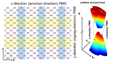
We consider phosphorene(BP monolayer) coated by periodic magnetic stripes along the plane direction as shown in Fig. 1. The magnetic field is applied perpendicular to the layer. The low-energy dispersion of bulk BP can be well described by a two band effective mass Hamiltonian due to the point group invariance LVoon ,
| (1) |
where , , are the two-band effective Hamiltonian, the RSOC term, the Zeeman term respectively. The first term is given by, RFei ; YJiang ; XZhou
| (2) |
The band parameters are , , , , , , , . The -direction periodic PMS induce periodic magnetic fields of pointing up and down sequentially. Accordingly the vector potential in each cell are given by,
| (6) | |||||
| (10) |
in which is the width of magnetic stripes. Similar form for -direction periodic PMS,
| (14) | |||||
| (18) |
Then we include only the most important anisotropic Rashba SOC term which is linear in momentum as given by Popovic ,
| (19) |
in which , , , and . Popovic The last term represents the familiar Zeeman effect. And therefore our full Hamiltonian is .
The envelope functions may be combined into a four component spinor which satisfies a Dirac equation . The electron wave functions are expanded in a plane wave basis confined by the large hard wall box. The wave function for electron can be expanded as
| (20) |
where () is the wave vector in the x (y) direction, and the expansion coefficient a four-component column vector. The wave function can be calculated numerically in the basis set with the periodic boundary conditions in the () direction.
The interaction Hamiltonian between the Dirac fermion and the photon within the electrical dipole approximation is , where the vector potential corresponds to the circularly polarized light. denotes the initial states in the lower cones that are hole or valence like, denotes the final states in the upper cone states that are electron of conduction like. Now the electron-light interaction induces transition from to , and are written as . The resulting optical transition rate of e-h pair between valence and conduction band is . The transition rate is given by,
| (21) |
in which . Finally we can obtain the optical absorption rate by the integral of transition rates in space,
| (22) |
III Numerical results and discussions
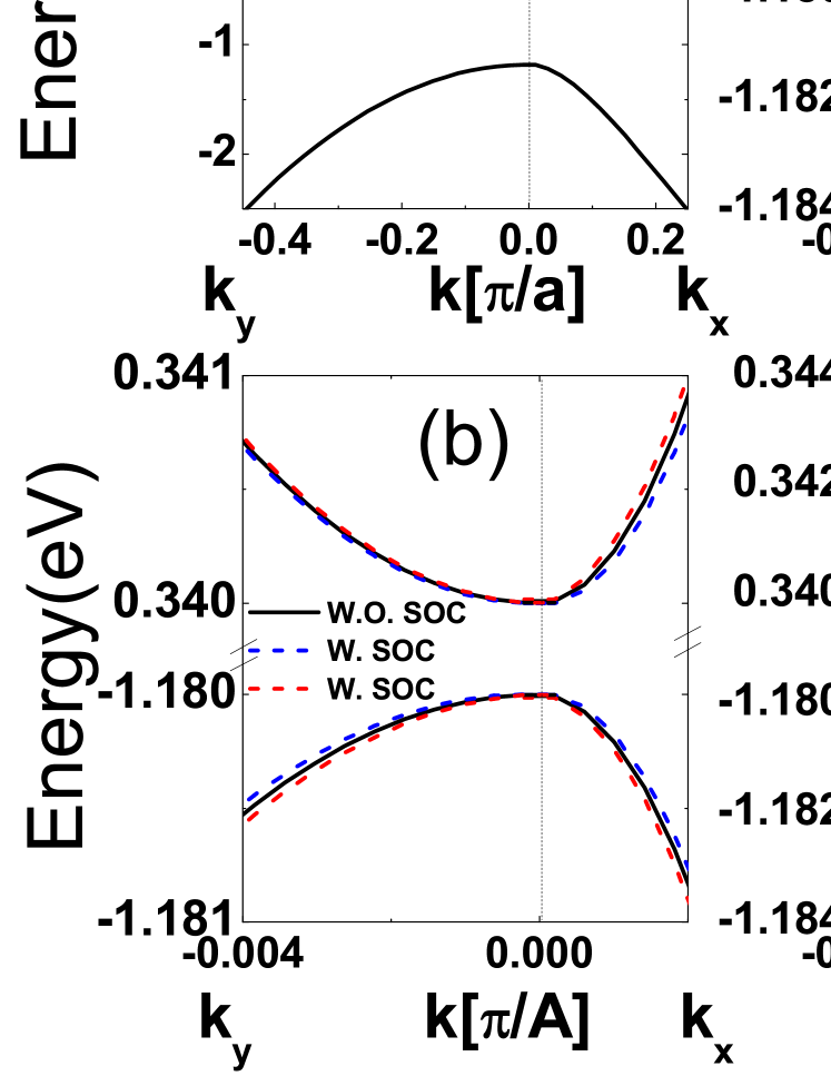
In pristine phosphorene parabolic energy bands reflect the existence of massive 2DEG with a direct band gap about eV at the point, being different from their counterparts of massless Dirac fermions in another well known 2D material graphene of hexagonal symmetry. The electron-hole symmetry is broken owing to the interband coupling. The conduction band valence band coupling effects influence the band structure effectively and lead to distinct electronic and optical properties rather than being observed in graphene. We start by investigating the energy dispersion relationships of a pristine phosphorene monolayer without any external magnetic field or with periodic magnetic field modulations along the direction (armchair direction) and the direction (zigzag direction) respectively. As sketched in Fig. 1, we find strongly PMS direction dependent energy bandgap enlargement, cone shift and dispersion modulation, which we will discuss below in details. First we plot the energy dispersions of pristine phosphorene in Fig. 2(a) and (b). Note that the different slopes of the energy dispersions along two orthogonal and directions indicate the anisotropic group velocities and effective masses in phosphorene (see Fig. 2(a)). This unique feature is also absent in graphene. When the RSOC interaction is incorporated into the calculations, we can find the expected spin splitting in the conduction and valence bands as shown by the dashed lines in Fig. 2(b). The spin splitting energy is proportional to the wave vector . Its impact on the band structure of phosphorene is very small near the point on the order of magnitude of 10 eV. The spin splittings due to the RSOC are also antitropic for conduction and valence bands.
Next we investigate the energy dispersions of a PMS with periodic orientations along the two orthogonal crystal axes, with fixed T, nm, nm. In Fig. 2, we can clearly see that the band minima are shifted away from the point along the transverse directions of the two type PMSs due to the time reversal symmetry breaking. To obtain a direct observation of energy dispersion modulation by PMS, we move the center of shifted energy cones back to point, see Fig. 2(c) - (f). When the periodic magnetic field varies along the direction, the energy dispersion of PMS with given magnetic fields is almost unchanged as compared to that of pristine phosphorene. Since the periodic perturbation on the off-diagonal interband coupling term is absence as indicated by Eq. 2 and 10. For a -direction PMS, i.e., the periodic magnetic field varies along the direction, the energy spectra in the wave vectors and are shown in Fig. 2(e) and (f). PMS show peculiar behaviors of gap modulation at the point. In conventional phosphorene superlattice with electric potentials, the energy gap is reduced Ono . Our proposal of magnetic phosphorene superlattices, however, are different in that the band gap is increased due to the external magnetic fields. The slopes of the conduction and valence energy bands decrease with the existence of magnetic field. Along the periodic direction, a small gap is opened at the boundary of each superlattice Brillouin zone, e.g. , due to the perturbation potentials coming from the periodic magnetic fields. In the transverse direction, the energy spectrum becomes slightly asymmetric with respect to , which is absence in phosphorene superlattice with electric potentials. It comes from the vector potentials accounting for time-reversal symmetry breaking by the magnetic fields, and therefore becomes more distinct as we increase the magnitude or the active area of the magnetic fields as we will discuss later. This feature is in consistent with previous studies on a single quantum well between two electric/magnetic/strain barriers ZWu1 ; ZWu2 ; ZWu3 . For a preliminary summary, the impacts of the PMS with different configurations on the energy dispersion relationships are quit distinct. The energy spectrum in -direction PMS (corresponding to the transport direction along the zigzag direction) is much more sensitive to the external periodic magnetic fields than that in its counterpart -direction PMS.
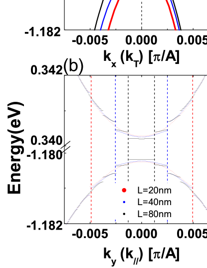
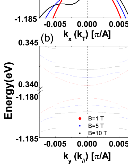
Then we focus on the energy dispersion and anisotropy modulation in -direction PMS, since its interband coupling term gives rise to more pronounced response to the periodic vector potential perturbations than that in -direction PMS. Heuristically, the magnetic fields tend to bend the carriers away from motion direction and thus suppress the group velocities of charge carriers as well as reduce energy dispersion. To get an quantitative assessment of the modulation effects on the electronic properties from the superlattice structure and magnetic field strength, we then plot the energy dispersions of -direction PMS along and with different periodic lengths and magnetic fields in Figs. 3 and 4. As the magnetic strip width increases, the aforementioned bi-directional anisotropy along the transversal direction (see Fig. 2(e)) becomes increasingly spectacular and develops two band minima being adjacent to the point as shown in Fig. 3(a). We note en passant that it is a magnetic field induced in-line anisotropy ZWu2 , rather than the intrinsic in-plane anisotropy in pristine phosphorene. Along the periodic direction, more band gaps are opened arising from the periodic perturbation effect at a reduced Brillouin zone boundary. When the periodic lengths is very large, the first subband is rather flat along the periodic direction, indicating the presence of heavy quasi particles in such a -direction PMS. While the energy dispersion along the transversal direction almost remains. Therefore the effective mass and anisotropy can be effectively tuned by the proposed PMS as shown in Fig. 3(c) and (d). Alternatively we can observe similar effects by increasing the strength of the magnetic fields. In addition band gap enlargement is more pronounced at the point and at superlattice Brillouin zone boundaries. This trend is in contrast with the periodic electrical potentials modulated phosphorene zhengli ; Ono .
So, the proposed PMS can effectively tune the anisotropy of energy dispersion and effective mass, since the energy dispersion along the transversal direction of the superlattice is almost immune to magnetic fields while the one along the longitude direction of the superlattice is effectively modulated. Beside the unique anisotropy between the highly anisotropic band structures along the two crystalline directions of phosphorence , in-line bidirectional anisotropy is induced by the magnetic fields. Importantly, here we address that modulation capabilities of different PMS periodic orientations are also highly anisotropic as we have discussed about Fig. 2. For the configuration of -direction (zigzag direction) PMS, bandstructures are more sensitively depend on the magnetic fields strength and periodic cell size .


Next we turn our focus to the carrier probability distributions in a unit cell of the PMS with different configurations. The projected charge distribution of the electrons in the first conduction band with certain and are shown in Fig. 5 and Fig. 6. With the wave vector along the magnetic strip (perpendicular to the periodic direction of the superlattice), the probability distributions exhibit anisotropic dependence on the wave vector as shown by solid lines in Fig. 5 (a) and (c) for -direction periodic and -direction periodic superlattice respectively. For a -direction (or -direction) PMS, the electrons from the first conduction band with positive (or ) tend to locate near the edges of a cell where no magnetic stripe is coated above. While for negative (or ), the electrons tend to locate in the center. This behavior directly arises from the Hall effect in the proposed PMS. Note that the spatial separation of electrons moving in the opposite direction is more pronounced with periodic magnetic modulations along the direction as shown in Fig. 5 (c). This feature is unique in phosphorene, since the effective vector potential () has distinct effects on the off—diagonal elements in Hamiltonian Eq. 2, while this impact is absence in -direction PMS. Along the superlattice direction, the probability distribution are isotropic for positive or negative wavevectors regardless -direction or -direction superlattice configurations (see Fig. 5 (b) and (d)). The electrons tend to distribute in the central region of a cell underneath the magnetic stripe. Since the perpendicular magnetic fields develop circular electron orbits and prevent them transmitting away. By incorporation the Zeeman term, we find that it has negligible impact on the energy spectrum but change the probability distribution apparently as shown by dashed lines in Fig. 5. In the plane wave basis, the diagonal matrix elements of Zeeman term are canceled out and the off-diagonal elements are imaginary numbers with the given periodic magnetic field profile. Therefore the Zeem term can hardly affect the eigenvalues but changes the eigenvector effectively. The RSOC term can also hardly affects the density distributions with wave vector along the direction of magnetic stripes as shown in Fig. 6 (a) and (c). But it tends to push the electrons with wave vector along the superlattice direction out of the phosphorene plane resulting in the squeezed distributions as shown in Fig. 6 (b) and (d).
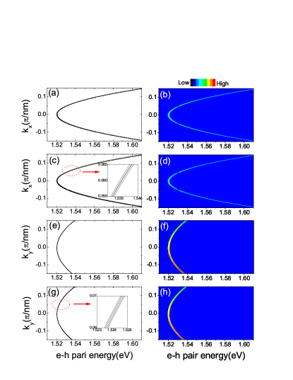
The anisotropy energy spectra and charge distributions are hard to measure directly. However they apparently can affect the Photoluminescence (PL) Spectra. We therefore investigate the effect of the PMS on the energy to form electron-hole (e-h) pairs by circularly polarized light and the transition rate. Figs.7 and 8 plot them as functions of the wave vector () with periodic magnetic field modulations along the () direction respectively. When considering the transition between two (accounting for both spin up and spin down states) highest valence bands to two lowest conduction bands, we can see the parabolic energy spectra of e-h pairs as shown in Fig. 7 (a), and the transition rates of low energy e-h pairs are isotropic in and rather bright when approaches . For larger away from it becomes dark arising from the electron distribution in the conduction and valence band with different as shown in Fig. 5 (c). When is not zero, the charge carriers from conduction bands or valence bands tend to locate along of the edge of a superlattice cell where no magnetic stripe is deposited above regardless of positive or negative . It results in small overlap integral of the wavefunctions and small transition rate in Fig. 7 (b). When approaches zero, the charge carriers tend to distribute equally in a superlattice and thus increase the overlap integral of the wavefunctions. Then the optical transition rate is enhanced. Next we examine the effect of the RSOC term, one can see the expected spin-splitting in the e-h pair energy spectrum (inset in Fig. 7 (c)). Accordingly the RSOC term can affect the electron distribution at the supperlattice BZ boundaries (Fig. 6 (c)) and reduce the transition rate spectrum of the low-energy e-h pairs, so we can find larger transition gap as shown in Fig. 7 (d). We also plot the e-h pair energy as function of in Fig. 7 (e), the asymmetrical behavior in the e-h pair energy spectrum is due to the anisotropic energy spectrum as shown in Fig. 2. The optical transition rate spectrum along () exhibits an in-line asymmetrical behavior with a dark-to-bright transition when the varies from negative to positive. The electrons with positive tend to locate aside the superlattice cell while the ones with negative tend to locate in the center as shown in Fig. 6 (a) and (b). Different distributions result in different overlap integral of wavefunctions and thus determine the optical transition rates as we observed. When the RSOC term is considered, we can find the spin splitting in the e-h pair energy and optical transition rate spectrum in 7 (g) and (h). The optical transition rate is enhanced the same as that in Fig. 7 (d) due to the same reason.
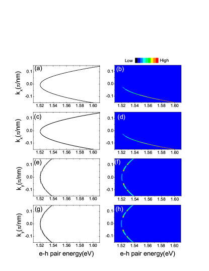
Compared to the -direction periodic PMS, the modulation effects by a -direction PMS are much more pronounced. The ground state e-h pairs energy as function of is asymmetrical due to the time-reversal symmetry breaking in the presence of a magnetic field as shown in Fig. 8 (a) and spin slitting due to the RSOC interaction in Fig. 8 (c). Because the electron with negative or positive shows separate distributions as shown in Fig. 5 (c) and 6 (c), we can find the dark-to-bright transition of the ground state e-h pair transition rate spectrum in Fig. 8 (b). The RSOC term has small effect on the transition rate spectrum in accounting for its limited impact on the electron distribution ( see Fig. 6 (b)). Corresponding e-h pair energy spectrum in are symmetrical as shown in Fig. 8 (e). The e-h pairs energy spectrum and optical transition rate spectrum of -direction periodic superlattice possess larger gaps at the supperlattice BZ boundaries as shown Fig. 8, due to the enhanced interband coupling by the vector potential of the PMS. The optical transition rate spectrum of the ground e-h pairs is not bright (see Fig. 8 (f)) due to the marginal distribution as shown in 6 (d), regardless whether is negative or positive. Although the spin splitting is shown in energy spectrum but can not been distinguished in the transition rate spectrum as shown in Figs. 8 (g) and (h). In brief summary, the optical transition rate of -direction PMS is different from that of -direction PMS as we discussed about Fig. 7. Obviously the anisotropy can be adjusted by the strength of the external magnetic field, the periodic length and the RSOC term. So we can realize an external field controlled magneto-optical device base on different PMS configurations.
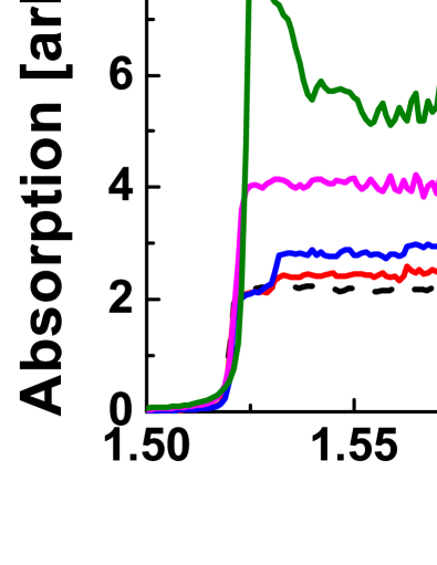
Finally the optical absorption spectrum of such a phosphorene magnetic supperlattice is calculated which can also be measured directly. In our calculation, we set the fermi level at zero energy which is between the conduction and valence band. It means the occupation for the valence band is full, while that for the conduction band it is empty. We use broadening factor of to smoothen the absorption spectrum. The optical absorption spectrum indicates useful band structure information guaranteed by the selection rule expressed as in Eq.21. In Fig. 9, Different configurations of periodic magnetic strips show different absorption characteristics. For a -direction periodic superlattice, the optical absorption spectrum with one wide step indicates transition rate enlargement arising from the charge distribution modulations as we discussed before. For a -direction PMS, we can find much higher absorption peak in low energy region and more oscillations when increasing the energy (frequency) of the incident light due to modulations from the -direction PMS. Increasing the magnetic field can also increase the absorption rate. The distinct optical absorption spectra provide an effective way to detect the anisotropic energy properties of PMS with different periodic orientations. The phosphorene magnetic supperlattice is a promising platform for potential application in anisotropic magneto-optical devices.
IV Conclusions
In this work, we theoretically investigate the electronic and optical properties of PMS utilizing the method. Our numerical results show that the anisotropic energy dispersions can be tuned by the PMS configurations, e.g., orientation, periodic length, strength. Accordingly the e-h pair energies also exhibit distinct differences between two configurations. We demonstrate that -direction (zigzag direction) superlattice gives rise to more pronounced modulation via the vector potential appeared in the electron-hole coupling term. As compared to the energy dispersion, charge distribution is much more sensitive to the external magnetic field or electric field (via RSOC). The magnetic fields and periodic orientations of the PMS proposed in this work play important roles in determining the e-h transition rates and optical absorption spectrum. Our theoretical results shed new light on potential applications of magneto-optical devices based on the anisotropic PMS.
Acknowledgements.
This work was supported by the MOST (Grants No. 2016YFA0202300) and the Opening Project of MEDIT, CAS.References
- (1) Esaki, L. and Tsu, R. Superlattice and Negative Differential Conductivity in Semiconductors. IBM Journal of Research and Development 14, 61 (1970).
- (2) Park, C. H. et al. Anisotropic behaviors of massless Dirac fermions in graphene under periodic potential. Nature Physics 4, 213 (2008).
- (3) Park, C. H. et al. Landau levels and quantum Hall effect in graphene superlattices. Phys. Rev. Lett. 103, 046808 (2009).
- (4) Brey, L. & Fertig, H. A. Emerging zero modes for graphene in a periodic potential. Phys. Rev. Lett. 103, 046809 (2009).
- (5) Barbier, M. et al. Extra Dirac points in the energy spectrum for superlattices on single-layer graphene. Phys. Rev. B 81, 075438 (2010).
- (6) Maksimova, G. M. et al. Graphene superlattice with periodically modulated Dirac gap. Phys. Rev. B 86, 205422 (2012).
- (7) Wu, Z., Li, J., and Chan, K. S. Charge pumping in monolayer graphene driven by a series of time-periodic potentials. Physics Letters A 376, 1159 (2012).
- (8) Uddin, S. & Chan, K. S. Band structure of ABC-trilayer graphene superlattice. J. Appl. Phys. 116, 203704 (2014).
- (9) Dell’Anna, L. & De Martino, A. Magnetic superlattice and finite-energy Dirac points in graphene. Phys. Rev. B 83, 155449 (2011).
- (10) Le, V. Q. et al. Magnetic Kronig-Penney-type graphene superlattices: finite energy Dirac points with anisotropic velocity renormalization. J. Phys.: Condens. Matter. 24, 345502 (2012).
- (11) Dell’Anna, L. et al. Using magnetic stripes to stabilize superfluidity in electron-hole double monolayer graphene. Phys. Rev. B 92, 220502(R) (2015).
- (12) Uddin, S. & Chan, K. S. Electric and magnetic superlattices in trilayer graphene. Physica E 75, 56 (2015).
- (13) Li, X., Wu, Z., and Liu, J. Rashba spin-orbit coupling in graphene monolayer coated by periodic magnetic stripes. Scientific Reports 7, 6526 (2017).
- (14) Li, L. et al. Black phosphorus field-effect transistors, Nat. Nanotechnol. 9, 372 (2014).
- (15) Morita, A. Semiconducting black phosphorus. Appl. Phys. A 39, 227 (1986).
- (16) Liu, H. et al. Phosphorene: An Unexplored 2D Semiconductor with a High Hole Mobility. ACS Nano 8, 4033 (2014).
- (17) Qiao, J. et al. Few-layer black phosphorus: emerging 2D semiconductor with high anisotropic carrier mobility and linear dichroism. Nature Communications 5,4475 (2014).
- (18) Wang, X. et al. Highly anisotropic and robust excitons in monolayer black phosphorus. Nature Nanotechnology 10, 517 (2015).
- (19) Vy Tran, Ryan Soklaski, Yufeng Liang, and Li Yang. Layer-Controlled Band Gap and Anisotropic Excitons in Phosphorene. Phys. Rev. B 89, 235319 (2014).
- (20) Xia, F. et al. Rediscovering black phosphorus as an anisotropic layered material for optoelectronics and electronics. Nature Communications 5, 4458 (2014).
- (21) Xie, Y. et al. Photogalvanic effect in monolayer black phosphorus. Nanotechnology 26, 455202 (2015).
- (22) X. Y. Zhou, R. Zhang, J. P. Sun, Y. L. Zou, D. Zhang, W. K. Lou, F. Cheng, G. H. Zhou, F. Zhai, and K. Chang. Landau levels and magnetotransport property of monolayer phosphorene. Sci. Rep. 5, 12295 (2015).
- (23) Popović, Z., Kurdestany, J., and Satpathy, S. Electronic structure and anisotropic Rashba spin-orbit coupling in monolayer black phosphorus. Physical Review B 92, 035135 (2015).
- (24) Wang, G., et al. Out-of-plane structural flexibility of phosphorene. Nanotechnology 27, 055701 (2016).
- (25) Li, Z., et al. Generation of Anisotropic Massless Dirac Fermions and Asymmetric Klein Tunneling in Few-Layer Black Phosphorus Superlattices. Nano Letters 17, 2280 (2017).
- (26) Shota Ono, Effect of one-dimensional superlattice potentials on the band gap of two-dimensional materials. J. Appl. Phys. 121, 204301 (2017).
- (27) Zhang, R., et al. Electronic and magneto-optical properties of monolayer phosphorene quantum dots. 2D Materials 2, 045012 (2015).
- (28) Zhou, X., et al. Anomalous magneto-optical response of black phosphorus thin films. Phys. Rev. B 92, 165405 (2015).
- (29) Zhou, X., et al. Effective g factor in black phosphorus thin films. Phys. Rev. B 95, 045408 (2015).
- (30) Li, L., et al. Quantum Hall effect in black phosphorus two-dimensional electron system. Nature Nanotechnology 11, 593 (2016).
- (31) Zhang, R., et al. Aharonov-Bohm effect in monolayer phosphorene nanorings. Phys. Rev. B 95, 125418 (2015)
- (32) Voon, L., et al. Effective Hamiltonians for phosphorene and silicene. New J. Phys. 17, 025004 (2015).
- (33) Fei, R., et al. Topologically protected Dirac cones in compressed bulk black phosphorus. Phys. Rev. B 91, 195319 (2015)
- (34) Jiang, Y., et al. Magnetoelectronic properties of multilayer black phosphorus. Phys. Rev. B 92, 085408 (2015)
- (35) Zhou, X., et al. Landau levels and magneto-transport property of monolayer phosphorene. Scientific Reports 5, 12295 (2015).
- (36) Wu, Z. Electronic fiber in graphene. Appl. Phys. Lett. 98, 082117 (2011).
- (37) Wu, Z., et al. Electron tunneling through double magnetic barriers on the surface of a topological insulator. Phys. Rev. B 82, 115211 (2010).
- (38) Wu, Z., et al. Valley-Dependent Brewster Angles and Goos-Ha nchen Effect in Strained Graphene. Phys. Rev. Lett. 106, 176802 (2011).